
 Open Access Article
 This Open Access Article is licensed under a Creative Commons Attribution-Non Commercial 3.0 Unported Licence
Fabrication of Ag2O/WO3 p–n heterojunction composite thin films by magnetron sputtering for visible light photocatalysis
Young Woong Jo†
a,
Chadrasekhar Loka†a,
Kee-Sun Lee *a and
Jae-Hyun Limb
*a and
Jae-Hyun Limb
aDepartment of Advanced Materials Engineering, Smart Natural Space Research Centre, Kongju National University, Cheonan-31080, South Korea. E-mail: kslee@kongju.ac.kr
bDepartment of Computer Science and Engineering, Kongju National University, Cheonan 331-717, South Korea
First published on 28th April 2020
Abstract
Semiconductor-based nanostructures which are photo-catalytically active upon solar light irradiation were extensively used for environmental remediation due to the potential decomposition of various kinds of pollutants. In this work, we report the preparation of a sustainable thin film composite, i.e. Ag2O/WO3 p–n heterojunction, and investigation of its photocatalytic activity. To achieve the composite structure, WO3/Ag–WO3 layers were deposited over a quartz substrate by magnetron sputtering at room temperature and subsequently annealed at 823 to 923 K. The thin film structure, morphology, and chemical states were thoroughly characterized by X-ray diffraction, field-emission scanning electron microscopy, transmission electron spectroscopy, and X-ray photoelectron spectroscopy. The obtained results revealed that the amorphous Ag-doped WO3 was crystallized into monoclinic WO3 and Ag2O, in which nanocrystalline Ag2O was diffused towards the surface of WO3. Optical transmittance spectra recorded by UV-vis-NIR spectroscopy revealed that the WO3/Ag–WO3 films became transparant in the visible region after annealing at high temperature (873 K and 923 K). The Ag2O/WO3 p–n heterojunction composite thin films showed high photocatalytic activity (0.915 × 10⁻³ min−1) under visible light irradiation, which is attributed to the efficiency of effective photogenerated charge-carrier formation and the reduced recombination rate of photogenerated electron–hole pairs. Unlike the powder-based photocatalysts, the reported thin film-based heterojunction photocatalyst could be very sustainable, and cost-effective.
1. Introduction
Recently, visible-light-driven photocatalysis has been regarded as an efficient renewable route for environmental remediation such as providing clean air and water sources by removing organic pollutants.1–4 In this regard, semiconductor-based photocatalysts, which can efficiently absorb and utilize visible light for the photodegradation of the organic compounds/molecules, have attracted much interest.5–8 Most of the studies have focused on anatase crystalline TiO2, which exhibits high photocatalytic activity and high chemical stability under ultraviolet (UV) light irradiation, the wavelength of which is below 387 nm with a respective energy bandgap of about 3.2 eV.9,10 Despite this, because of its wide optical bandgap TiO2 can only utilize 5% of the solar spectrum (UV light). In contrast, investigations of the visible light driven photocatalytic materials are emerging because of their efficient use of a large proportion (44%) of the solar spectrum. Tungsten oxide (WO3), an n-type semiconductor with an optical bandgap of 2.6 to 2.8 eV exhibits particularly promising photocatalytic performance under visible light (λ > 380 nm).11,12 In addition, WO3 is well known for its stable physicochemical properties, good thermal stability, and resilience to photocorrosion effects.13,14 However, pure WO3 is having limitations such as low conduction band level, which inhibits the ability to react with electron acceptors. Moreover, the fast recombination rate of photogenerated electron–hole is the major limitation to its ability of photocatalytic efficiency.15 Therefore, strenuous efforts have been devoted to improve the photocatalytic activity of the semiconductor-based photocatalyst such as controlling the particle size, crystal structure, composition, and loading a small amount of noble metals such as Ag, Au, and Pt to WO3.16–20Nevertheless, in recent years, the fabrication of heterojunction structures was considered as an ingenious approach and the most viable long-term solution with the potential to degrade the environmental pollutants. Bai et al. detailed the charge kinetics and mechanism in the n–n heterojunction and p–n heterojunction photocatalysts.21 The p–n heterojunction structures were proven faster transmission of photogenerated holes, which is quite significant to improve the photocatalytic activity by facilitating electron–hole separation.21–27 Thus, several researchers reported various p–n heterojunction photocatalysts such as α-Fe2O3/Cu2O,6 Ag2O/Bi2O2CO3,28 Ag3PO4/WO3,29 Fe3O4/Bi2O2CO3,30 TiO2/NiO,27 WO3/Ag2CO3,31 and WO3/BiOI.32 Irrespective of the strategy that was implemented to improve the photocatalytic activity, most of these studies are powder-based photocatalytic materials. Despite, the investigations on thin film based photocatalysts have been rarely reported. For advanced photocatalytic applications, it is essential to eliminate the separation activity in which the powder-based photocatalysts need repeated separation process from the polluted water. Therefore, the design of an efficient thin film coating-based photocatalysts which can easily separate the electron–hole pair that exhibits promising photocatalytic activity without any additional separation procedures, unlike the powder-based photocatalysts is the emerging for sustainable practical environmental applications. Various physical methods have been reported to fabricate WO3 thin films such as sol–gel, electrodeposition, atomic layer deposition, dip-coating, thermal evaporation and sputtering.33–38 Among these techniques, the magnetron sputtering is a unique method for the fabrication of large-scale high-quality thin film coatings.
In this work, we propose a novel sputter-deposited p–n heterojunction thin film nanostructures formed by Ag2O and WO3 in which Ag2O nanosheet-like structures embedded in the monoclinic WO3 phase for an efficient photocatalytic activity under visible light irradiation by suppressing the recombination rate of photogenerated electron–hole pairs. Ag2O, a p-type direct bandgap semiconductor with a reported optical bandgap ∼1.46 eV,39 which can be suitable to form a prominent p–n heterojunction with WO3 due to its high efficiency, controllability and ease of fabrication. For example, Zhou et al. has demonstrated a high photocatalytic activity with a p–n heterojunction formed by Ag2O/TiO2 nanobelts driven both UV and visible light for the degradation of methyl orange (MO).40 Similarly, Ag2O-based heterojunction structures Ag2O/BiWO6,41 Ag2O/g-C3N4,42 Ag2O/Ag2CO3,43 Ag2O/CeO2,44 ZnO/Ag2O,45 and Ag2O/Bi2MoO6 (ref. 46) were successfully demonstrated by the other researchers for visible light photocatalysis. In this work, nanosheet-like Ag2O was chosen with the combination of WO3 because it is advantageous in not only improving the photocatalytic activity but also allows the thin film apparently transparent due to the homogeneous spatial distribution of Ag2O in WO3. The visible-light-driven photocatalytic activity of the WO3/Ag–WO3 films was evaluated by the photodegradation of methylene blue (MB), and the relations with enhanced photocatalytic properties and microstructure evolution were investigated.
2. Experimental section
Tungsten oxide thin films were deposited over the quartz glass substrate with a WO3 target of 99.999% purity (2 in diameter) at room temperature by using radio frequency (RF) magnetron sputtering. Prior to sputtering, the base pressure of the sputtering chamber was pumped down to 2 × 10⁻⁶ Torr using a turbomolecular pump. Argon (Ar) of 99.999% purity was used as a sputtering gas, 230 sccm Ar gas was input into the chamber through the mass flow controller. Sputtering power 150 W was supplied to the target, and distance between the sputter target and the substrate was fixed at 90 mm. Ag-doped (Ag–WO3) films were prepared by sputtering with a mosaic target in which small Ag chips (2 chips, size: 1 mm × 1 mm × 0.5 mm) embedded over the surface of the WO3 target. The same sputtering conditions were maintained for both the pure WO3 films and Ag–WO3 films. Finally, WO3/quartz and WO3/Ag–WO3/quartz thin films were deposited and subsequently annealed at 823 K to 923 K in air ambient for 1 h using a Rapid Thermal Annealing (RTA) system.The structural properties of the films were investigated by using X-ray diffraction (XRD) with Bruker X-ray diffractometer using Cu-Kα radiation (λ = 1.5406 Å), the X-ray source was operated at 40 kV and 30 mA. The UV-visible absorbance spectra and transmittance spectra were recorded in the range of 300 to 1000 nm by using UV-vis-NIR spectrophotometer (UV-3600, Shimadzu, Japan). The surface morphology and cross-sectional structure of the thin films were investigated by using field-emission scanning electron microscopy (FESEM, TESCAN MIRA3, Korea). Thin film cross-section was investigated by transmission electron microscopy (TEM, Tecnai G2 F20, Thermo Fisher, USA) with energy dispersive X-ray (EDX) analyzers, the samples were prepared by a focused ion-beam system for the TEM observation. X-ray photoelectron spectroscopy (XPS) was carried out using Al Kα X-ray with constant analyzer mode. The photoluminescence properties were studied by using a PerkinElmer LS-50B luminescence spectrometer. Photocatalytic activity of the prepared thin films was investigated by measuring the degree of decomposition of methylene blue (20 ml MB solution, 10 ppm) under visible light illuminated by Xe-lamp 500 W with a 400 nm filter. To maintain the constant temperature of the MB solution, cooled water was continuously circulated via double-walled photoreactor. The photocatalytic degradation of MB has been evaluated from the decrease in the absorption intensity of MB at the wavelength of 664 nm. The photocatalytic degradation efficiency has been evaluated using the following equation.
3. Results and discussion
X-ray diffraction pattern of the as-deposited and annealed WO3 thin films at different temperatures (823 K, 873 K, and 923 K) in air ambient for 1 h were shown in Fig. 1(a). In the case of as-deposited films, no peaks were detected which are associated with the WO3 indicating that the amorphous nature of the films in the form of WO3−x. This may be attributed to the room temperature deposition because the adatoms may not acquire enough energy to initiate their crystal lattice orientation on the glass substrates.47 After annealing, the films exhibited polycrystalline nature and all the peaks were associated to the monoclinic phase of WO3 corresponding to JCPDS 83-0950 (space group P21/n(14); lattice parameters a = 7.3008 Å, b = 7.5389 Å, and c = 7.6896 Å; β = 90.892°). The major XRD peak with a predominant reflection observed at 2θ = 24.37° corresponding with a preferred orientation (200) plane of monoclinic crystal structure, while the other peaks were indexed as (002), (020), (220), (222), (400), and (420) plane which are in good agreement with the previously reported sputter-deposited WO3 films.48 X-ray diffraction pattern of Ag–WO3/WO3 films was shown in Fig. 1(b), the as-deposited films exhibited amorphous nature with no trace of XRD peaks. Irrespective of the annealing temperature, the preferred orientation (200) of WO3 remains unchanged with the addition of Ag but diffraction peak intensity of the (002) plane corresponding to WO3 became more intense for the annealed films. | ||
| Fig. 1 X-ray diffraction patterns of the (a) WO3/quartz glass, (b) WO3/Ag–WO3/quartz glass. | ||
Fig. 2 shows the surface morphology of the WO3 films observed by FESEM at 50k× magnification. The surface morphology of as-deposited WO3 thin film films exhibited densely packed nano-sized WO3 grains. After annealing at 823 K, the densely packed amorphous films were crystallized with clear grain boundaries. By further increasing the annealing temperature to 923 K, non-uniform large polycrystalline grains were formed with increased grain boundaries, which could be plausibly due to the merging of small grains during the annealing process.
 | ||
| Fig. 2 FESEM images (magnification: 50k×) of as-deposited and annealed WO3 thin films surface morphology: (a) as-deposited, (b) 823 K, (c) 873 K, and (d) 923 K. | ||
FESEM images of the WO3/Ag–WO3 thin films annealed at different temperatures were shown in Fig. 3. The as-deposited films exhibited smooth surface morphology. However, very small nanorod-like structures were observed on the surface of the WO3/Ag–WO3 films annealed at 823 K. Nevertheless, it can be observed that the morphology of these nanorod-like structure was evolved in the type of nanosheet at 873 K and they became much more defined as the annealing temperature increased to 923 K. In addition, the surface morphology of 873 K annealed films comprised of a large number of nanosheets with lower spatial distribution in comparison with the 923 K films. The nanosheet-like structure formation was plausible due to the outward diffusion of Ag through the grain boundaries of WO3. From the surface morphology, it is evident that the 873 K films possess small grain boundaries of WO3 compared to the 923 K films. Thus, the presence of nanosheets over the 873 K films surface is much higher than 923 K films. Kumar et al. reported that the grain boundary diffusivity of the metal at metal/metal-oxide interface is extremely fast,49 which supports for the formation of Ag nanostructures over the surface of WO3. With an increase in annealing temperature to 873 K, the diffused nanosheet-like Ag2O structures were drastically changed into the randomly oriented collectively grown nanosheet due to the agglomeration and grain growth of similar nanosheet-like structures. The evolution of nanosheets was continued to grow anisotropically because various crystal plane directions can be collectively grown and dominated due to the difference in the grain growth rates along that particular direction which leads to the possible shapes of the Ag nanostructures such as sheet-like, plate-like and rod-like shapes.
 | ||
| Fig. 3 High (10k×) and low-magnification (1k×) FESEM images of as-deposited and annealed WO3/Ag–WO3 thin films surface morphology: (a) as-deposited, (b) 823 K, (c) 873 K, and (d) 923 K. | ||
Obviously, the directional growth of nanosheets observed in FESEM surface morphology images of the WO3/Ag–WO3 films annealed at 823 to 973 K reflects that the Ag grain growth was definite which also represent the oxidation possibility of the Ag. The formation of Ag–O during the deposition of initial layer Ag–WO3 on quartz substrate can be inevitable and the detailed mechanism can be explained as follows. Irradiation of high energetic Ar+ at 45° could lead to the sputtering ejection of W, O, and Ag atoms from the Ag-chip embedded WO3 target, which arrives at the substrate and the substrate get covered with the W, O, and Ag atoms depend on their sputtering yields. Fundamentally, this process involves adsorption, desorption, and diffusion of the sputter-deposited atoms, wherein the possibility of diffusion and clustering of the sputter-deposited atoms leads to the formation of Ag–O in the growing film. However, due to the low concentration of Ag and absence of substrate heating, Ag–O formation cannot be significant enough to exhibit crystallinity. Upon annealing the films in air ambient at high temperature, the amorphous Ag-doped WO3 phase was transformed to crystalline Ag2O + WO3 phase, agglomeration and outward diffusion of Ag2O was pronounced to form large grains in the form of Ag2O nanosheets through the WO3 grain boundaries. Thus, the Ag2O/WO3 composite phase formation could be observed in the WO3/Ag–WO3 films after annealing at high temperatures.
For a more detailed understanding of the evolution of collectively grown Ag2O nanosheets, thin film cross-section of the WO3/Ag–WO3 after and before annealing was observed as shown in Fig. 4. As shown in Fig. 4(a), the as-deposited films exhibited a very clear interface between Ag–WO3 and WO3 layers. The evolution of collectively grown nanosheets can be clearly observed from the FESEM cross-section image Fig. 4(b). Obviously, the interface between the substrate and thin film is intact which indicates good adhesion of the annealed films at 923 K, while the interface of WO3 and Ag–WO3 was disappeared due to the mixing of WO3 phases and outward diffusion of Ag during the annealing process. In order to confirm the existence of Ag, the WO3/Ag–WO3 films annealed at 923 K were subjected to FESEM EDS (energy dispersive X-ray spectrometry) analysis and respective elemental mapping along with elemental distribution of Ag and W were shown in Fig. 4(c). Thus, the elemental mapping substantiated that the final microstructure of the films comprised of collectively grown Ag2O nanosheets embedded WO3 composite structure.
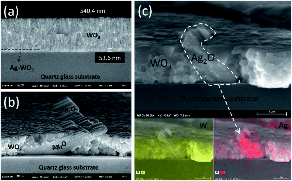 | ||
| Fig. 4 FESEM images of WO3/Ag–WO3 thin films: (a) cross-section of the as-deposited films, (b) cross-section of the annealed films at 923 K, (c) cross-section of backscattering image and EDS elemental mapping of W and Ag corresponding to the annealed films at 923 K. | ||
The structure of the WO3/Ag–WO3 films annealed at 923 K was further characterized by TEM analysis. Fig. 5(a) shows the cross-section microstructure, which confirms the formation of nanocrystalline WO3 grains. Fig. 5(b) shows the selected area electron diffraction (SAED) pattern indexed properly with the monoclinic structure of WO3. As shown in Fig. 5(c), the high-resolution TEM (HR-TEM) image revealed the clear lattice fringes with an interplanar spacing about 0.364 and 0.376 nm which are corresponding to the (200) and (020) planes of the monoclinic–WO3, respectively. Darkfield STEM (DF STEM) elemental scanning images obtained from the EDX exhibit the distribution of the constituted elements W, O, and Ag as shown in Fig. 5(d). The presence of a substantial amount of Ag across the WO3 layer confirmed the outward diffusion of Ag through WO3 grain boundaries. These results are in good accordance with the results observed by the FESEM analysis (Fig. 4(c)).
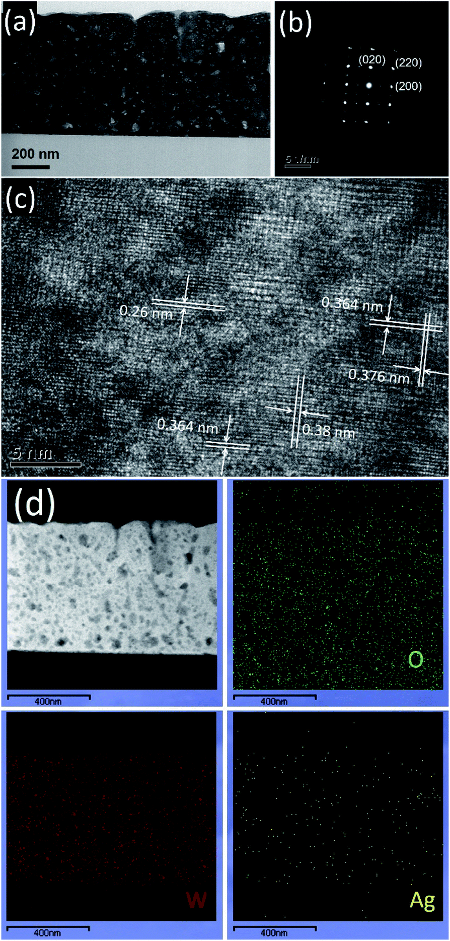 | ||
| Fig. 5 TEM images of WO3/Ag–WO3 films annealed at 923 K: (a) cross-sectional microstructure, (b) SAED pattern of WO3, (c) HR-TEM image with clear crystalline planes of monoclinic–WO3 phase, and (d) DF STEM image and corresponding EDX elemental distribution of W, O, and Ag. | ||
Optical absorbance spectra of the films were measured in the UV-vis region of wavelength range 300 to 900 nm. The optical bandgap was evaluated by using the following equation.50–53
| ∝hv = A(hv − Eg)n |
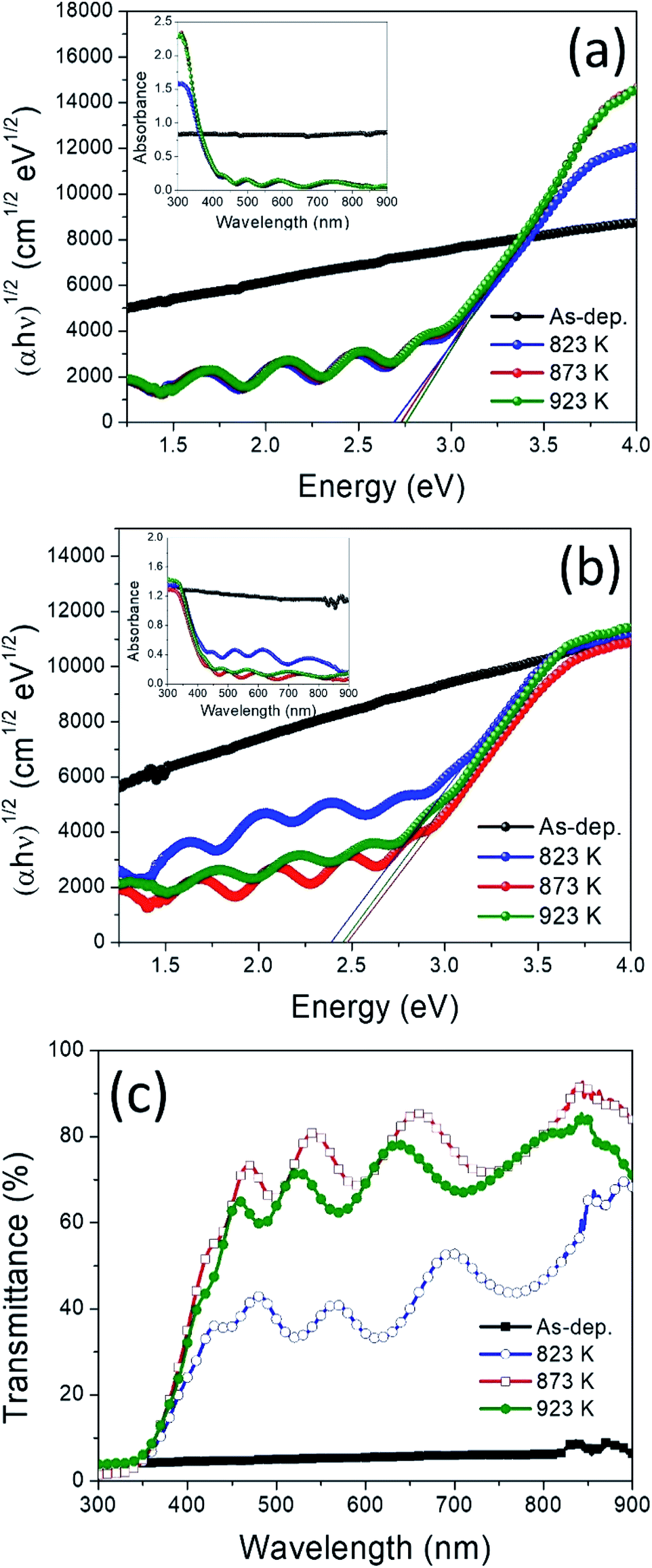 | ||
| Fig. 6 (αhν)1/2 vs. hν plots and absorbance spectra of the WO3 films (a), and WO3/Ag–WO3 films (b); optical transmittance spectra of the as-deposited and annealed WO3/Ag–WO3 films (c). | ||
The surface chemical states and compositions of the as-deposited and annealed (923 K) WO3/Ag–WO3 films were analysed by using the X-ray photoelectron spectroscopy. The XPS full-scan survey spectrum of the films was shown in Fig. 7(a), the annealed films clearly exhibit the presence of Ag, W, O peaks, and the as-deposited films show W and O peaks. High-resolution XPS spectra of W 4f were deconvoluted and shown in Fig. 7(b), the spin–orbit doublet for W valence state i.e. W 4f5/2 and 4f7/2 are attributed to the binding energy values of 38.07 and 36.14, 34.55 eV, respectively.57,58 The doublet 4f5/2 and 4f7/2 splitting is 2.13 eV, position and shape of the peaks appeared (38.07 and 36.14 eV) were representative of an oxidation state of W6+ for the WO3−x.59 As shown in Fig. 7(c), the oxygen 1s peak occurred in the as-deposited films at 531.0 eV corresponding to WO3 and 532.1 eV attributed to the hydroxylation (W–OH).58 In the case of annealed films, the peaks at 35.21 and 33.86 eV are corresponding to the W 4f7/2, and 37.16 eV belongs to the W 4f5/2 (Fig. 7(d)). The spin–orbit splitting is 2.1 eV with peaks area ratio 3![[thin space (1/6-em)]](https://www.rsc.org/images/entities/char_2009.gif) :4 for W 4f5/2 and 4f7/2. The O 1s peak centred at 530.5 eV is ascribed to the formation of a strong W
:4 for W 4f5/2 and 4f7/2. The O 1s peak centred at 530.5 eV is ascribed to the formation of a strong W![[double bond, length as m-dash]](https://www.rsc.org/images/entities/char_e001.gif) O bond.60 In contrast, based on the fitting of W 4f peaks, the annealed films consist of 84% of the W6+ while compared to the as-deposited films which show only 64%. Such an observation indicates that the annealed films comprised of the stoichiometric WO3 phase, while the as-deposited films are under-stoichiometric WO3−x phase with higher surface oxygen vacancies. The doublet of Ag 3d was deconvoluted as shown in Fig. 7(f). The peaks identified at 367.5, 368.1 and 373.6 eV were assigned to the Ag 3d5/2 and Ag 3d3/2 of Ag in Ag2O, respectively. The splitting of the Ag 3d doublet was 6.0 eV, which indicates that the Ag exists in the form of the Ag2O phase.
O bond.60 In contrast, based on the fitting of W 4f peaks, the annealed films consist of 84% of the W6+ while compared to the as-deposited films which show only 64%. Such an observation indicates that the annealed films comprised of the stoichiometric WO3 phase, while the as-deposited films are under-stoichiometric WO3−x phase with higher surface oxygen vacancies. The doublet of Ag 3d was deconvoluted as shown in Fig. 7(f). The peaks identified at 367.5, 368.1 and 373.6 eV were assigned to the Ag 3d5/2 and Ag 3d3/2 of Ag in Ag2O, respectively. The splitting of the Ag 3d doublet was 6.0 eV, which indicates that the Ag exists in the form of the Ag2O phase.
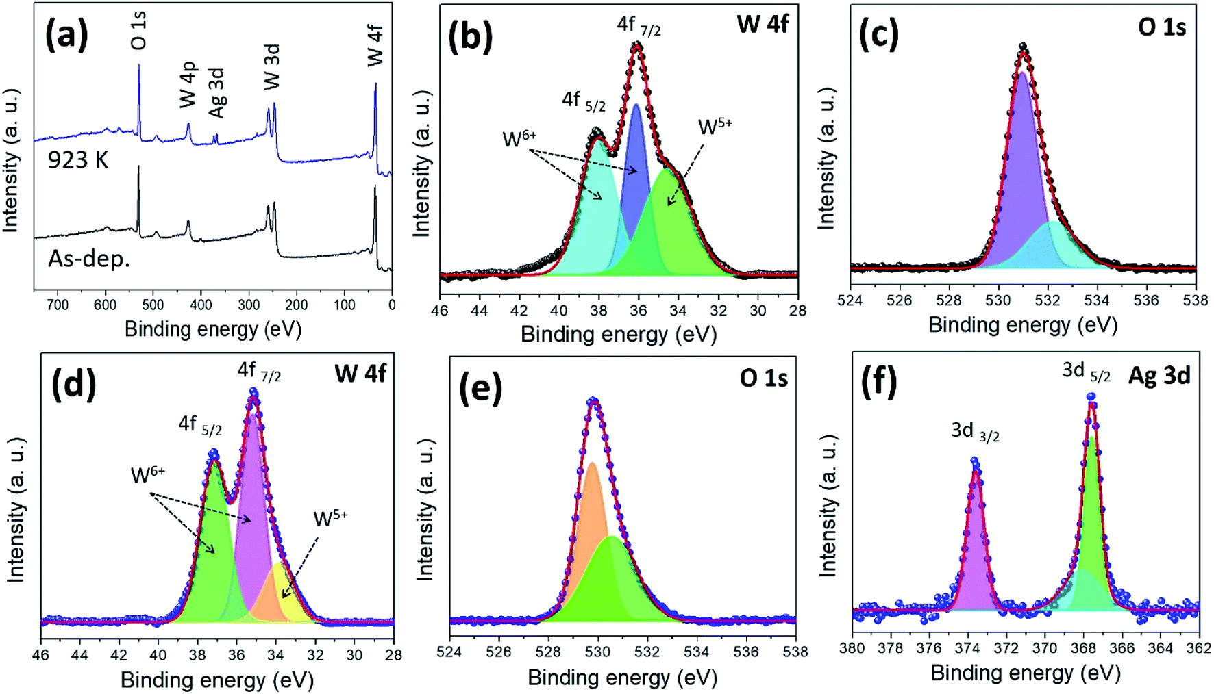 | ||
| Fig. 7 X-ray photoelectron spectra of the WO3/Ag–WO3 films and peak fitting: wide-scan spectra of as-deposited and annealed films (a), high-resolution scan of W and O for as-deposited films (b and c), high-resolution scan of W, O, and Ag for annealed films at 923 K (d, e, and f). | ||
The photocatalytic activities of the WO3 and WO3/Ag–WO3 (i.e. Ag2O/WO3 composite) films were evaluated by determining the photodegradation of the methylene blue under the irradiation of visible light, the photocatalytic performance was shown in Fig. 8(a). Annealed films at 923 K for 30 min in air ambient, which are in the monoclinic phase were utilized for the evaluation of the photocatalytic activity. The pseudo-first-order kinetic equation was used to calculate the reaction rate constant (k).

 | ||
| Fig. 8 (a) Photocatalytic performance of the WO3 and WO3/Ag–WO3 films, photodegradation of methylene blue under the irradiation of visible light; the reaction rate constants were calculated based on the pseudo-first-order reaction kinetics. (b) Schematic illustration of the photocatalytic mechanism of Ag2O/WO3 p–n heterojunction photocatalyst, and (c) photoluminescence emission spectra of the WO3/Ag–WO3 films. | ||
The reaction rate constant (k) of WO3 and Ag2O/WO3 composite films are 2.39 × 10⁻³ min−1 and 0.915 × 10⁻³ min−1, respectively. The Ag2O nanosheets embedded WO3 composite films exhibited 2.61 times higher photocatalytic activity than that of pure WO3 films. The obtained results clearly demonstrated that the Ag2O nanosheets exhibited a vital effect on the photocatalytic activity of WO3 films, which can be due to the formation of p–n heterojunction Ag2O of WO3. A schematic of Ag2O/WO3 was shown in Fig. 8(b), p–n heterojunction forms when p-type Ag2O and n-type WO3 were contacted, the net electrons will migrate into Ag2O from WO3 while the net holes will migrate from WO3 to Ag2O until the Fermi level reaches equilibrium conditions (Ef = 0.807 eV). Because of these electron and hole migration, an electric field built at the interface between Ag2O and WO3. Under the irradiation of visible light, not only WO3 generates electron–hole pairs but the narrow bandgap Ag2O (Eg = 1.4 eV) also excites to generate electron–hole pairs. Due to the existence of the barrier between the Ag2O and WO3 heterojunction, the migration of photogenerated charge carriers would be promoted as shown in the schematic Fig. 8(b). Consequently, the probability of charge carrier recombination can be decreased, and a large number of holes can be accumulated on the Ag2O while the electrons can be concentrated on WO3. The pure WO3 shows very little (∼20%) degradation of the pollutants due to relatively lower conduction band edge of WO3 (+0.3–0.5 V vs. NHE) which is insufficient to provide the required potential for the single-electron reduction of O2 (EO2/O2− = −0.33 V vs. NHE; EO2/HO2˙ = −0.55 V vs. NHE).61 In the case of Ag2O/WO3 p–n heterojunction, the electrons accumulated at conduction band of WO3 would be transferred to surface-adsorbed oxygen molecules to form H2O2 by multi-electron reduction of O2. The photoinduced holes with high oxidation potential (+3.1 V vs. NHE) are apt to react with surface-bound H2O or OH− to produce hydroxyl radical species ˙OH which is extremely strong oxidant for the degradation of organic contaminants. Thus, the photocatalytic reactions would be triggered to decompose the methylene blue with enhanced photocatalytic activity in WO3/Ag–WO3 films annealed at 923 K. The enhanced photocatalytic activity associates with the reduction of recombination rate of photogenerated charge carriers. Therefore, to determine the charge migration and extent of electron–hole pair recombination i.e. electron–hole pair separation ability, the photoluminescence spectra of the WO3/Ag–WO3 films was studied as shown in Fig. 8(c). As shown in the figure, the emission ranges between 375–600 nm. The emission of photons resulting from the electron–hole pair recombination gives the photoluminescence spectra. In general, the sample with high luminous peak intensity represents the faster recombination of electron–hole pairs in that sample, whereas the sample with low luminous peak intensity represents the prolonged life-time of the photogenerated charge carriers. Therefore, the high intensity of the emission peaks for as-deposited and annealed films below 873 K corresponds to higher charge carrier recombination. These strong emission peaks are induced by the electron–hole radiation recombination due to the de-excitation from W6+ to O2−. The films annealed at 923 K exhibit lower emission peak intensity which indicate the lowest charge carrier recombination among all the films. Therefore, the Ag2O/WO3 composite films in which Ag2O nanosheets were homogeneously embedded in WO3 exhibited significant photocatalytic activity is ascribed to the efficient charge transfer process in the films. Thus, the films offer a superior photocatalytic activity than that of pure WO3 films. Although this Ag2O/WO3 thin film composite p–n heterojunction structure has attained better photocatalytic activity than pure WO3, further study is required to achieve high photocatalytic activity to compete with powder-based photocatalysts because true potential of this structure is fully unrealized due to the reason of low available surface area for the photocatalytic reaction. This work would provide a sustainable, reusable, simple and cost-effective thin film based photocatalyst, and it would have widespread applications in the future for environmental remediation.
4. Conclusions
Semiconductor photocatalysts of p-type Ag2O and n-type WO3 were suitably designed to form thin film p–n heterojunction by RF magnetron sputtering and subsequent annealing of Ag–WO3/WO3 thin films for the application of visible-light photocatalysis. Upon annealing, the amorphous WO3 was converted to monoclinic WO3. Thin film surface and cross-section observations revealed that the Ag2O has been diffused outward towards the surface of WO3, the chemical composition investigated by XPS also confirmed the existence of the Ag2O phase on WO3 surface. The Ag2O/WO3 composite films obtained after annealing at 923 K exhibited about 66% transmittance in the visible region, and the photoluminescence emission spectra results revealed that the films possess lowest electron–hole recombination rate among all the films. The photocatalytic activity of the obtained Ag2O/WO3 p–n heterojunction thin film composed of Ag2O nanosheets embedded WO3 composite was evaluated by degradation of MB solution under visible light, the films exhibited 2.61 times higher photocatalytic activity than that of pure WO3 films with a photocatalytic activity rate constant of 0.915 × 10⁻³ min−1. The enhanced photocatalytic activity of p–n heterojunction attributed to the good visible light absorption and efficient separation of photogenerated electron–hole pairs. This work provides a unique approach to design optically transparent, environmentally sustainable, reusable, simple and cost-effective thin film p–n heterojunction photocatalysts with better photocatalytic activity for visible-light photocatalysis by controlling the separation of photogenerated electron–hole pairs and homogeneous distribution of photocatalysts in nano-size.Conflicts of interest
There are no conflicts to declare.Acknowledgements
This work was supported by the Priority Research Centers Program through the National Research Foundation of Korea (NRF) funded by the Ministry of Education (2019R1A6A1A03032988). This research was supported by the International Science and Business Belt Program through the Ministry of Science and ICT (2015-DD-RD-0068-05).Notes and references
- M. A. Shannon, P. W. Bohn, M. Elimelech, J. G. Georgiadis, B. J. Marĩas and A. M. Mayes, Nature, 2008, 452, 301–310 CrossRef CAS PubMed.
- T. P. Yoon, M. A. Ischay and J. Du, Nat. Chem., 2010, 2, 527–532 CrossRef CAS PubMed.
- D. M. Schultz and T. P. Yoon, Science, 2014, 343, 1239176 CrossRef PubMed.
- G. S. Das, J. P. Shim, A. Bhatnagar, K. M. Tripathi and T. Y. Kim, Sci. Rep., 2019, 9, 1–9 CrossRef PubMed.
- H. Wang, L. Zhang, Z. Chen, J. Hu, S. Li, Z. Wang, J. Liu and X. Wang, Chem. Soc. Rev., 2014, 43, 5234–5244 RSC.
- J.-C. Wang, L. Zhang, W.-X. Fang, J. Ren, Y.-Y. Li, H.-C. Yao, J.-S. Wang and Z.-J. Li, ACS Appl. Mater. Interfaces, 2015, 7, 8631–8639 CrossRef CAS PubMed.
- N. S. Gultom, H. Abdullah, D. H. Kuo and W. C. Ke, ACS Appl. Energy Mater., 2019, 2, 3228–3236 CrossRef CAS.
- J. Li, Y. Liu, Z. Zhu, G. Zhang, T. Zou, Z. Zou, S. Zhang, D. Zeng and C. Xie, Sci. Rep., 2013, 3, 2–7 Search PubMed.
- X. Chen and S. S. Mao, Chem. Rev., 2007, 107, 2891–2959 CrossRef CAS PubMed.
- K. Nakata and A. Fujishima, J. Photochem. Photobiol., C, 2012, 13, 169–189 CrossRef CAS.
- S. Cong, F. Geng and Z. Zhao, Adv. Mater., 2016, 28, 10518–10528 CrossRef CAS PubMed.
- T. T. Nguyen, S. N. Nam, J. Son and J. Oh, Sci. Rep., 2019, 9, 1–18 CrossRef PubMed.
- S. Adhikari, K. Sarath Chandra, D. H. Kim, G. Madras and D. Sarkar, Adv. Powder Technol., 2018, 29, 1591–1600 CrossRef CAS.
- T. Kako, X. Meng and J. Ye, APL Mater., 2015, 3, 104411 CrossRef.
- Y. Kong, H. Sun, W. Fan, L. Wang, H. Zhao, X. Zhao and S. Yuan, RSC Adv., 2017, 7, 15201–15210 RSC.
- X. Liu, H. Zhai, P. Wang, Q. Zhang, Z. Wang, Y. Liu, Y. Dai, B. Huang, X. Qin and X. Zhang, Catal. Sci. Technol., 2019, 9, 652–658 RSC.
- P. Dong, G. Hou, X. Xi, R. Shao and F. Dong, Environ. Sci.: Nano, 2017, 4, 539–557 RSC.
- H. Katsumata, Y. Oda, S. Kaneco and T. Suzuki, RSC Adv., 2013, 3, 5028–5035 RSC.
- A. Tanaka, K. Hashimoto and H. Kominami, J. Am. Chem. Soc., 2014, 136, 586–589 CrossRef CAS PubMed.
- O. Arutanti, A. B. D. Nandiyanto, T. Ogi, T. O. Kim and K. Okuyama, ACS Appl. Mater. Interfaces, 2015, 7, 3009–3017 CrossRef CAS PubMed.
- S. Bai, J. Jiang, Q. Zhang and Y. Xiong, Chem. Soc. Rev., 2015, 44, 2893–2939 RSC.
- L. Yang, S. Luo, Y. Li, Y. Xiao, Q. Kang and Q. Cai, Environ. Sci. Technol., 2010, 44, 7641–7646 CrossRef CAS PubMed.
- Z. Zhang, C. Shao, X. Li, C. Wang, M. Zhang and Y. Liu, ACS Appl. Mater. Interfaces, 2010, 2, 2915–2923 CrossRef CAS PubMed.
- C. Chen, W. Cai, M. Long, B. Zhou, Y. Wu, D. Wu and Y. Feng, ACS Nano, 2010, 4, 6425–6432 CrossRef CAS PubMed.
- S. Ida, A. Takashiba, S. Koga, H. Hagiwara and T. Ishihara, J. Am. Chem. Soc., 2014, 136, 1872–1878 CrossRef CAS PubMed.
- M. Long, W. Cai, J. Cai, B. Zhou, X. Chai and Y. Wu, J. Phys. Chem. B, 2006, 110, 20211–20216 CrossRef CAS PubMed.
- M. Wang, Y. Hu, J. Han, R. Guo, H. Xiong and Y. Yin, J. Mater. Chem. A, 2015, 3, 20727–20735 RSC.
- N. Liang, M. Wang, L. Jin, S. Huang, W. Chen, M. Xu, Q. He, J. Zai, N. Fang and X. Qian, ACS Appl. Mater. Interfaces, 2014, 6, 11698–11705 CrossRef CAS PubMed.
- L. You, M. Gao, T. Li, L. Guo, P. Chen and M. Liu, New J. Chem., 2019, 43, 17104–17115 RSC.
- G. Zhu, M. Hojamberdiev, K. I. Katsumata, X. Cai, N. Matsushita, K. Okada, P. Liu and J. Zhou, Mater. Chem. Phys., 2013, 142, 95–105 CrossRef CAS.
- M. Gao, L. You, L. Guo and T. Li, J. Photochem. Photobiol., A, 2019, 374, 206–217 CrossRef CAS.
- J. Luo, X. Zhou, L. Ma and X. Xu, J. Mol. Catal. A: Chem., 2015, 410, 168–176 CrossRef CAS.
- O. Prakash, V. Saxena, S. Choudhury, A. Tanvi, A. Singh, A. K. Debnath, A. Mahajan, K. P. Muthe and D. K. Aswal, Electrochim. Acta, 2019, 318, 405–412 CrossRef CAS.
- M. Covei, C. Bogatu, D. Perniu, A. Duta and I. Visa, Ceram. Int., 2019, 45, 9157–9163 CrossRef CAS.
- T. Brezesinski, D. F. Rohlfing, S. Sallard, M. Antonietti and B. M. Smarsly, Small, 2006, 2, 1203–1211 CrossRef CAS PubMed.
- J. Xue, Y. Zhu, M. Jiang, J. Su and Y. Liu, Mater. Lett., 2015, 149, 127–129 CrossRef CAS.
- R. S. Vemuri, K. K. Bharathi, S. K. Gullapalli and C. V. Ramana, ACS Appl. Mater. Interfaces, 2010, 2, 2623–2628 CrossRef CAS PubMed.
- L. Weinhardt, M. Blum, M. Bär, C. Heske, B. Cole, B. Marsen and E. L. Miller, J. Phys. Chem. C, 2008, 112, 3078–3082 CrossRef CAS.
- Y. Ida, S. Watase, T. Shinagawa, M. Watanabe, M. Chigane, M. Inaba, A. Tasaka and M. Izaki, Chem. Mater., 2008, 20, 1254–1256 CrossRef CAS.
- W. Zhou, H. Liu, J. Wang, D. Liu, G. Du and J. Cui, ACS Appl. Mater. Interfaces, 2010, 2, 2385–2392 CrossRef CAS PubMed.
- H. Yu, R. Liu, X. Wang, P. Wang and J. Yu, Appl. Catal., B, 2012, 111–112, 326–333 CrossRef CAS.
- H. T. Ren, S. Y. Jia, Y. Wu, S. H. Wu, T. H. Zhang and X. Han, Ind. Eng. Chem. Res., 2014, 53, 17645–17653 CrossRef CAS.
- C. Yu, G. Li, S. Kumar, K. Yang and R. Jin, Adv. Mater., 2014, 26, 892–898 CrossRef CAS PubMed.
- X. J. Wen, C. G. Niu, L. Zhang, C. Liang and G. M. Zeng, Appl. Catal., B, 2018, 221, 701–714 CrossRef CAS.
- S. Ma, J. Xue, Y. Zhou and Z. Zhang, J. Mater. Chem. A, 2014, 2, 7272–7280 RSC.
- J. Zhang, H. Liu and Z. Ma, J. Mol. Catal. A: Chem., 2016, 424, 37–44 CrossRef CAS.
- R. Sivakumar, R. Gopalakrishnan, M. Jayachandran and C. Sanjeeviraja, Opt. Mater., 2007, 29, 679–687 CrossRef CAS.
- Y. Zhao, S. Balasubramanyam, R. Sinha, R. Lavrijsen, M. A. Verheijen, A. A. Bol and A. Bieberle-Hütter, ACS Appl. Energy Mater., 2018, 1, 5887–5895 CrossRef CAS.
- A. Kumar, H. Barda, L. Klinger, M. W. Finnis, V. Lordi, E. Rabkin and D. J. Srolovitz, Nat. Commun., 2018, 9, 5251 CrossRef CAS PubMed.
- M. A. Butler, J. Appl. Phys., 1977, 48, 1914–1920 CrossRef CAS.
- A. Subrahmanyam and A. Karuppasamy, Sol. Energy Mater. Sol. Cells, 2007, 91, 266–274 CrossRef CAS.
- R. S. Vemuri, M. H. Engelhard and C. V. Ramana, ACS Appl. Mater. Interfaces, 2012, 4, 1371–1377 CrossRef CAS PubMed.
- N. Li, H. Teng, L. Zhang, J. Zhou and M. Liu, RSC Adv., 2015, 5, 95394–95400 RSC.
- Y. He, Z. Wu, L. Fu, C. Li, Y. Miao, L. Cao, H. Fan and B. Zou, Chem. Mater., 2003, 15, 4039–4045 CrossRef CAS.
- S. Meng, W. Sun, S. Zhang, X. Zheng, X. Fu and S. Chen, J. Phys. Chem. C, 2018, 122, 26326–26336 CrossRef CAS.
- K. Ghosh, A. Roy, S. Tripathi, S. Ghule, A. K. Singh and N. Ravishankar, J. Mater. Chem. C, 2017, 5, 7307–7316 RSC.
- M. Vasilopoulou, A. Soultati, D. G. Georgiadou, T. Stergiopoulos, L. C. Palilis, S. Kennou, N. A. Stathopoulos, D. Davazoglou and P. Argitis, J. Mater. Chem. A, 2014, 2, 1738–1749 RSC.
- M. A. Arvizu, H. Y. Qu, U. Cindemir, Z. Qiu, E. A. Rojas-González, D. Primetzhofer, C. G. Granqvist, L. Österlund and G. A. Niklasson, J. Mater. Chem. A, 2019, 7, 2908–2918 RSC.
- D. Gogova, K. Gesheva, A. Szekeres and M. Sendova-Vassileva, Phys. Status Solidi A, 1999, 176, 969–984 CrossRef CAS.
- J. Li, J. Zhu and X. Liu, New J. Chem., 2013, 37, 4241–4249 RSC.
- G. S. Jamila, S. Sajjad, S. A. K. Leghari and M. Long, J. Hazard. Mater., 2020, 382, 121087 CrossRef CAS PubMed.
Footnote |
| † Authors contributed equally to this manuscript. |
| This journal is © The Royal Society of Chemistry 2020 |