DOI:
10.1039/D0RA01434F
(Paper)
RSC Adv., 2020,
10, 11166-11172
Scanning atmospheric-pressure plasma jet treatment of nickel oxide with peak temperature of ∼500 °C for fabricating p–i–n structure perovskite solar cells†
Received
26th November 2019
, Accepted 11th March 2020
First published on 17th March 2020
Abstract
Scanning atmospheric-pressure plasma jet (APPJ) treatment of nickel oxide with a peak temperature of 500 °C was performed for fabricating p–i–n structure perovskite solar cells (PSCs). APPJ post-treatment increases the haze of NiO on FTO glass, leading to enhanced light scattering in PSCs that in turn improves the cell efficiency. APPJ treatment on NiO also improves the wettability to facilitate the follow-up deposition of CH3NH3PbI3. This also leads to better PSC performance. X-ray photoelectron spectroscopy indicates that APPJ treatment results in fewer C–N bonds and reduced NiAc2 content, suggesting more complete conversion of the liquid precursor into NiO. With three APPJ scans, the average PCE improves from 11.91% to 13.47%, with the best-performing PSC achieving an efficiency of 15.67%.
1. Introduction
Recently, organic–inorganic hybrid perovskite solar cells (PSCs) have been developed rapidly owing to their excellent properties.1–5 The power conversion efficiency (PCE) of PSCs has been improved rapidly to 25.2%6–10 within a decade. In fact, their PCE exceeds that of CIGS- and CdTe-based solar cells and is already comparable to that of Si-based single-junction solar cells.11,12
The hole transport layer (HTL) plays important roles in hole collection, hole transportation, and electron-blocking; therefore, optimizing the HTL for matching energy levels, enhancing light transmittance, and improving interfacial compatibility is essential for realizing good PSCs. NiO is a widely used HTL for a p–i–n PSC. NiO has a high work function (∼5.1 eV) and deep valence band (∼5.4 eV). Furthermore, it is chemically more stable compared with poly(3,4-ethylenedioxythiophene)-poly(styrenesulfonate) (PEDOT:PSS). Typical deposition techniques used for NiO are sol–gel process,13,14 sputtering,15,16 pulsed laser deposition,17,18 and spray pyrolysis.19,20 The fill factor (F.F.) and short circuit current (Jsc) of PSCs with an NiO HTL were reported to be relatively low owing to the lower conductivity of NiO and poor contact between NiO and the perovskite layer. To overcome these problems, surface modification and doping are investigated to improve the performance of a PSC with an NiO HTL. Ag, Cu, Li, and Cs are the typical dopants introduced to NiO for improving its p-type conductivity and band alignment;21–26 interfacial modification is also applied to improve PSC performance.27
Low-pressure plasma (LPP) has been widely applied in industry for thin-film deposition and etching. However, generating LPP requires vacuum chamber and vacuum pumps that are costly and require routine maintenance. It is also disadvantageous to integrate with non-vacuum device fabrication procedures and roll-to-roll processes. By contrast, atmospheric-pressure plasma (APP) can be operated at a regular pressure and has shown promise in applications such as clinical medication, agriculture, and materials syntheses and surface modification.28–31 Typical APP technology includes gliding arc, corona discharge, dielectric barrier discharge, and atmospheric pressure plasma jet (APPJ). Recent developments have resolved problems such as continuous arcing, high breakdown voltage, and instability.32–34 APPJ with medium temperature (400–700 °C) has demonstrated rapid materials processing capability owing to the synergetic effect of reactive plasma species and heat.35–38
In this study, a scan-mode nitrogen DC-pulse APPJ is used to treat NiO for PSCs. The peak temperature of the substrate during APPJ operation is ∼500 °C. The optical transmittance, haze spectra, surface morphology, chemical bonding configuration, wettability, conductivity, and electrochemical properties of scanning APPJ-treated NiO are characterized. PSCs with scanning APPJ-treated NiO also show improved performance compared to samples with only 10 min hot plate treatment, with PCE increasing from 11.91% to 13.47%; Jsc from 16.96 mA to 17.55 mA cm−2; and F.F. from 68.56% to 73.66%.
2. Experimental section
2.1. Fabrication of PSC
Deionized water, acetone, and isopropanol were used sequentially to rinse the FTO glass substrate (TEC7, ∼8 Ω sq−1) with ultrasonication for 15 min each. Next, the FTO substrate was treated by UV–ozone for 15 min. The precursor solution for the NiO film was prepared with 0.5 M nickel acetate (99.998%, trace metal basis, Sigma-Aldrich) and ethanolamine (99.5%, Sigma-Aldrich) dissolved in ethanol; the solution was stirred overnight at 60 °C.39 A liquid precursor film was spin-coated on the FTO glass substrate for 40 s at 6000 rpm, following which the liquid-precursor-film-coated sample was calcined at 325 °C for 10 min for APPJ-treated NiO samples. The thickness of the resultant NiO was ∼30 nm. An NiO thin-film-coated FTO glass substrate was thus obtained. After natural cooing to room temperature, the NiO film was treated by a nitrogen APPJ in scanning mode three times. The counterpart samples without APPJ treatment on NiO films were calcined at 325 °C on a hot plate for 10 and 90 min. Next, we transferred the samples into a nitrogen-filled glove box immediately for follow-up CH3NH3PbI3 depositions. The perovskite film was deposited by a one-step process. The CH3NH3PbI3 solution included 1.2 mM CH3NH3I (MAI, 98%, Dyesol) and PbI2 (99.999%, trace metal basis, Alfa Aesar) dissolved in dimethylformamide (DMF, 99.8%, Sigma-Aldrich). The resultant solution was spin-coated on NiO at 5000 rpm for 30 s; during the spin-coating process, 200 μl of CB was dripped rapidly onto the sample after starting spinning for 7 s. Next, the sample was calcined at 100 °C for 10 min to form a dense perovskite film (thickness: ∼350 nm). PC61BM (nano-C, 20 mg ml−1 in chlorobenzene) was doped with 2 μl of N,N-dimethyl-N-octadecyl(3-aminopropyl)trimethoxysilyl chloride silane (DMOAP, Sigma-Aldrich, 42 wt% in methanol). The DMOAP-doped PC61BM solution was spin-coated at 2000 rpm for 30 s.40 Then, bathocuproine (BCP, Alfa Aesar, 0.5 mg ml−1 in 2-propanol) was spin-coated at 6000 rpm for 20 s, following which it was dried at 85 °C for 15 min. Finally, 85 nm-thick Ag with area of 0.09 cm2 was deposited on the sample using an e-beam evaporator.
2.2. APPJ treatment on NiO
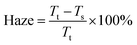
Fig. S1† shows the schematic of the APPJ equipment used in this study. The NiO film was first annealed at 325 °C for 10 min, following which it was treated by an APPJ in scanning mode three times with a scanning speed of 0.2 cm s−1. The details of the APPJ system are described elsewhere.41 A Pyrex™ tube with 4.8 cm length with 3 cm internal diameter was installed downstream of the plasma jet; the end of this tube was ∼1 mm above the substrate. This tube is used for minimizing the ambient air-quenching effect while allowing the high-rate gas to flow out smoothly. APPJ operation was performed with N2 flow rate of 46 slm to realize peak substrate temperature of 500 °C. Fig. 1 shows the representative temperature evolution of the FTO glass during three APPJ scans. The peak temperature is set to be ∼500 °C by adjusting the tube length and flow rate. The temperature was measured by a K-type thermocouple. The counterpart samples without APPJ treatment on NiO films were calcined at 325 °C on a hot plate for 10 and 90 min.
 |
| | Fig. 1 Temperature evolution of substrate under APPJ operation. | |
2.3. Characterization of NiO films and PSCs
The surface morphology of NiO was examined using scanning electron microscopy (SEM, JOEL, JSM-7800Prime) and atomic force microscopy (AFM, Bruker, BioScope Resolve). The ultraviolet-visible (UV-vis) transmittance and reflectance were measured by a UV-vis spectrophotometer (JASCO, V-670), and the through-plane (perpendicular to the film surface) conductivity was measured by an electrometer (Keithley 2636A). The sample for conductivity measurement was FTO glass/NiO/Ni structure, in which Ni was used for ohmic contact. A contact angle goniometer (Sindatek, Model 100SB) was used to measure the water contact angle. The surface chemical bonding status and elemental composition were analyzed using X-ray photoelectron spectroscopy (XPS, Thermo Fisher Scientific, ESCALAB Xi+). The Current density–voltage (J–V) curves of the PSC were measured using a sourcemeter (Agilent, B2902A) under illumination of simulated AM1.5 light (ABET, Sun 2000 Solar Simulator). For J–V curves, both forward and reverse scans were measured and forward scan was measured first. Electrochemical impedance spectroscopy was performed using an electrochemical workstation (EIS, Metrohm-Autolab, PGSTAT204) from 1 MHz to 1 Hz.
3. Results and discussion
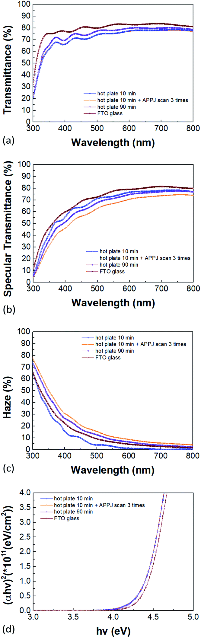
Fig. 2(a) shows the total transmittance spectra; the total transmittance remains similar after the APPJ treatment. Fig. 2(b) and (c) show plots of the specular transmittance and haze spectra, respectively. The specular transmittance reduced after APPJ treatment. The haze was calculated as42| |
 | (1) |
where Tt is the total transmittance and Ts, the specular transmittance. The two total transmittance curves, for the samples with bare 10 min hot plate calcination and 10 min hot plate plus three APPJ scans, almost overlap with only ∼1% difference. APPJ treatment apparently increased the haze of the NiO coated FTO. This could increase the forward light scattering as light passes through the NiO-coated FTO. Fig. 2(d) shows the Tauc bandgap that is calculated as43where α is the absorption coefficient; A, a constant; hν, the photon energy; and Eg, the optical bandgap; further, n = 2 refers to the direct bandgap of NiO. The measured band gap was ∼4.37 eV; this agrees with the previously reported data.25,44
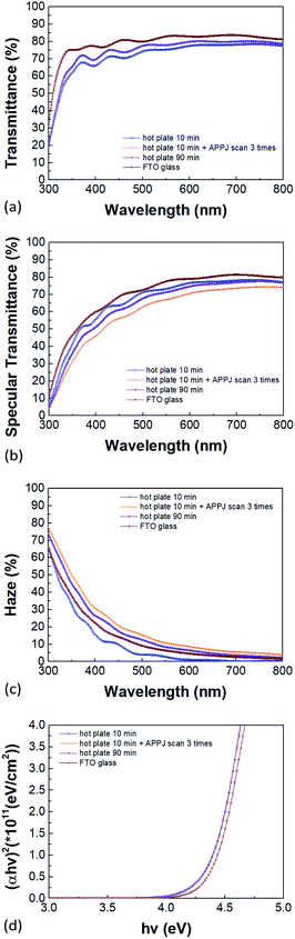 |
| | Fig. 2 UV-vis spectra of NiO film on FTO glass: (a) total transmittance spectra, (b) specular transmittance spectra, (c) haze spectra and (d) Tauc plot. | |
The surface coverage and crystallinity of the perovskite layer have been reported to be pivotal for the device performance.45 Fig. 3(a)–(c) show the AFM measurement results for NiO-coated FTO under different NiO treatment conditions and Fig. 3(d)–(f) show the corresponding SEM measurement results of CH3NH3PbI3 coated NiO on FTO. After APPJ treatment, the roughness increased from ∼23 nm to ∼25 nm. This could enhance the forward light scattering to improve the cell efficiency,13,46 thus agreeing well with the haze spectra shown in Fig. 2(c). Fig. 3(d)–(f) show SEM images of the CH3NH3PbI3 films. The CH3NH3PbI3 films are dense and well-crystallized. Fig. S2† shows SEM images of cross sections of the films; the films look compact in these views.
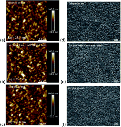 |
| | Fig. 3 AFM images of FTO/NiO structure (a–c) and SEM of FTO/NiO/CH3NH3PbI3 structure (d–f) with NiO (a and d) 10 min hot plate treatment, (b and e) 10 min hot plate plus three APPJ scans, and (c and f) 90 min hot plate treatment. | |
Fig. 4 and 5 show the XPS C 1s and Ni 2p3/2 binding energy spectra for NiO films. The C–C bond peak was adjusted to 284.5 eV; the main peaks for C 1s are located at 284.5, 285.9, 286.5, 287.8, and 289.1, and they respectively correspond to C–C, C–N, C–O, C![[double bond, length as m-dash]](https://www.rsc.org/images/entities/char_e001.gif) O, and C(O)O.47,48 The C–N bond can be ascribed to the ethanolamine residue (left from liquid precursor) after calcination. Table S1† shows the deconvoluted peak areal fractions. After APPJ treatment, the C–N content decreased significantly; simultaneously, the C–O content increased. As for the Ni 2p3/2 spectra (Fig. 5), the main peaks at 852.2, 853.8, 855, 855.4, 855.8, and 856.8 respectively correspond to Ni, NiO, Ni(OH)2, NiAc2, NiOOH and Ni2O3.10,49,50 Table S2† lists the areal fractions of deconvoluted peaks. The sample subjected to 10 min hot plate treatment shows relatively high NiAc2 content owing to the incomplete transformation of the liquid precursor into the NiO film. Similar phenomena were also observed in other studies.13,39 After APPJ treatment, the NiO content increased and NiAc2 content apparently decreased, suggesting that APPJ treatment can further convert precursor residue into NiO.
O, and C(O)O.47,48 The C–N bond can be ascribed to the ethanolamine residue (left from liquid precursor) after calcination. Table S1† shows the deconvoluted peak areal fractions. After APPJ treatment, the C–N content decreased significantly; simultaneously, the C–O content increased. As for the Ni 2p3/2 spectra (Fig. 5), the main peaks at 852.2, 853.8, 855, 855.4, 855.8, and 856.8 respectively correspond to Ni, NiO, Ni(OH)2, NiAc2, NiOOH and Ni2O3.10,49,50 Table S2† lists the areal fractions of deconvoluted peaks. The sample subjected to 10 min hot plate treatment shows relatively high NiAc2 content owing to the incomplete transformation of the liquid precursor into the NiO film. Similar phenomena were also observed in other studies.13,39 After APPJ treatment, the NiO content increased and NiAc2 content apparently decreased, suggesting that APPJ treatment can further convert precursor residue into NiO.
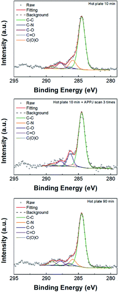 |
| | Fig. 4 XPS C 1s spectra of NiO film with different treatment. | |
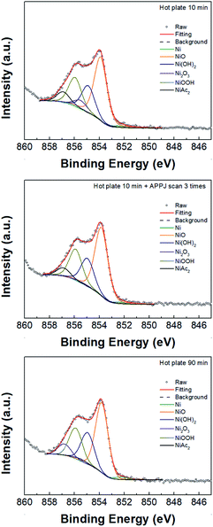 |
| | Fig. 5 XPS Ni 2p3/2 spectra of NiO film with different treatment. | |
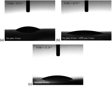
Fig. 6 shows the water contact measurement results. The water contact angle of 10 min hot plate treated NiO was ∼29°. After APPJ treatment, the water contact angle decreased to ∼18°. In comparison, the water contact angle of 90 min hot plate treated NiO was ∼21°. The wettability of NiO could influence the grain size and crystallinity of the follow-up deposited CH3NH3PbI3. These, in turn, will change the trap density of the CH3NH3PbI3 film.51–53
 |
| | Fig. 6 Water contact angles of NiO films with (a) 10 min hot plate treatment, (b) 10 min hot plate and three APPJ scans, and (c) 90 min hot plate treatment. | |
Fig. 7(a) shows the through-plane conductivity of the NiO films. APPJ treatment slightly increased the NiO conductivity from 1.98 × 10⁻³ mS cm−1 to 2.10 × 10⁻³ mS cm−1. It is speculated that a higher amount of ethanolamine residue results in reduced NiO film conductivity, as evidenced in the XPS experiment. Fig. 7(b) shows the J–V curves of the best-performing PSC with 10 min hot plate treatment and three APPJ scans. The PSC efficiency reached 15.67%. Fig. 7(c)–(f) shows statistical plots of the photovoltaic parameters of six batches of PSCs and Table 1 lists the corresponding statistics of PV parameters for reverse scans. As shown in Table 1, the PSC with NiO subjected to 10 min hot plate and three APPJ scans exhibited the highest average Jsc, F.F. and PCE; these parameters improved from 16.96 mA cm−2, 68.56%, and 11.91% to 17.55 mA cm−2, 73.66%, and 13.47%, respectively. The increased F.F. and Jsc can be attributed to the increased haze of NiO on FTO, improved wettability, and increased through-plane conductivity. The PSC performance with APPJ treatment also surpasses those with 90 min hot plate treatment. This indicates that APPJ treatment can improve the PSC performance with less processing time.
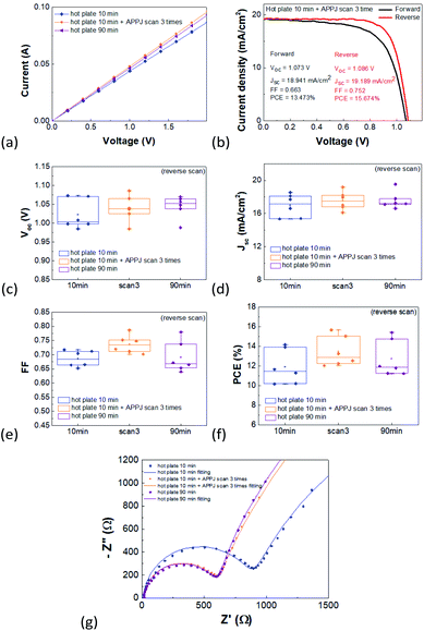 |
| | Fig. 7 (a) Current–voltage curve (conductivity) measured through NiO plane. (b) J–V curves of the best-achieving PSC. Statistical plots for (c) Voc, (d) Jsc, (e) FF, and (f) PCE for six batches of PSCs. (g) Nyquist plots for EIS measurement. | |
Table 1 PV parameters of PSCs
| |
Voc (V) |
Jsc (mA cm−2) |
FF |
PCE (%) |
| Hot plate 10 min |
1.02 ± 0.04 |
16.96 ± 1.38 |
68.56 ± 3.24 |
11.91 ± 1.76 |
| Hot plate 10 min + three APPJ scans |
1.04 ± 0.03 |
17.55 ± 1.11 |
73.66 ± 5 |
13.47 ± 1.54 |
| Hot plate 90 min |
1.04 ± 0.03 |
17.59 ± 1.03 |
69.09 ± 5.50 |
12.74 ± 1.86 |
EIS measurements were also performed under illumination to investigate the internal charge transporting and recombination through the devices.54 Fig. S3† shows the fitting model circuit.55 Fig. 7(g) shows the Nyquist plot with the fitting parameters listed in Table 2. R1, R2, and R3 represent the series resistance, charge transporting resistance, and recombination resistance, respectively. Clearly, R2 decreased (lower charge transport resistance) after APPJ treatment due to the higher surface roughness and conductivity. Further, the enhanced wettability of NiO with APPJ treatment may enhance the crystallinity of the follow-up CH3NH3PbI3 with lower grain boundaries and trap densities, thereby inhibiting the non-radiative recombination related to R3.
Table 2 EIS
| |
R1 (Ω) |
R2 (Ω) |
CPE2-T (F) |
CPE2-P |
R3 (Ω) |
CPE3-T (F) |
CPE3-P |
| Hot plate 10 min |
16.87 |
743.9 |
6.930 × 10⁻⁹ |
1 |
4930 |
3.6265 × 10⁻⁶ |
0.73 |
| Hot plate 10 min + three APPJ scans |
17.64 |
558.1 |
6.71 × 10⁻⁹ |
1 |
8052 |
1.4596 × 10⁻⁶ |
0.82 |
| Hot plate 90 min |
19.19 |
557.9 |
6.550 × 10⁻⁹ |
1 |
6864 |
1.1682 × 10⁻⁶ |
0.85 |
4. Summary
Scanning APPJ treatment on NiO with peak temperature of 500 °C can improve the performance of p–i–n PSCs. APPJ treatment increases the haze of the NiO film, leading to the improved forward light scattering that in turn improves the efficiency of the PSC. APPJ treatment could also improve the wettability of NiO to facilitate the follow-up deposition of CH3NH3PbI3. XPS shows fewer C–N bonds and NiAc2 content after APPJ treatment, indicating enhanced conversion of the liquid precursor conversion into NiO. A PSC with NiO subjected to 10 min hot plate and three APPJ scans exhibited the highest average Jsc, F.F. and PCE; these parameters improved from 16.96 mA cm−2, 68.56%, and 11.91% to 17.55 mA cm−2, 73.66%, and 13.47%, respectively.
Conflicts of interest
There are no conflicts to declare.
Acknowledgements
We gratefully acknowledge the funding support from the Ministry of Science and Technology of Taiwan under grant no. MOST 108-2221-E-002-088-MY3. This work is also financially supported by the “Advanced Research Center for Green Materials Science and Technology” from the Featured Area Research Center Program of the Higher Education Sprout Project by the Ministry of Education (108L9006) and the Ministry of Science and Technology in Taiwan (MOST 108-3017-F-002-002). We would like to specially thank Ms. Yuan-Tze Lee for her help with the SEM operation. The facility support from the Nano-Electro-Mechanical-Systems (NEMS) Research Center at National Taiwan University, Taiwan is also gratefully acknowledged.
Notes and references
- P. Gao, M. Gratzel and M. K. Nazeeruddin, Energy Environ. Sci., 2014, 7, 2448–2463 RSC.
- P. P. Boix, K. Nonomura, N. Mathews and S. G. Mhaisalkar, Mater. Today, 2014, 17, 16–23 CrossRef CAS.
- H. Choi, J. Jeong, H. B. Kim, S. Kim, B. Walker, G. H. Kim and J. Y. Kim, Nano Energy, 2014, 7, 80–85 CrossRef CAS.
- A. Kojima, K. Teshima, Y. Shirai and T. Miyasaka, J. Am. Chem. Soc., 2009, 131, 6050–6051 CrossRef CAS PubMed.
- Q. Dong, Y. Fang, Y. Shao, P. Mulligan, J. Qiu, L. Cao and J. J. Huang, Science, 2015, 347, 967–970 CrossRef CAS PubMed.
- S. Ryu, J. Seo, S. S. Shin, Y. C. Kim, N. J. Jeon, J. H. Noh and S. I. Seok, J. Mater. Chem. A, 2015, 3, 3271–3275 RSC.
- J. Burschka, N. Pellet, S. J. Moon, R. Humphry-Baker, P. Gao, M. K. Nazeeruddin and M. Gratzel, Nature, 2013, 499, 316–319 CrossRef CAS PubMed.
- M. L. Jiang, J. M. Wu, F. Lan, Q. Tao, D. Gao and G. Y. Li, J. Mater. Chem. A, 2015, 3, 963–967 RSC.
- M. M. Lee, J. Teuscher, T. Miyasaka, T. N. Murakami and H. J. Snaith, Science, 2012, 338, 643–647 CrossRef CAS PubMed.
- Z. A. Tan, W. Q. Zhang, D. P. Qian, C. H. Cui, Q. Xu, L. J. Li, S. S. Li and Y. F. Li, Phys. Chem. Chem. Phys., 2012, 14, 14217–14223 RSC.
- National Renewable Energy Laboratory, https://www.nrel.gov/pv/cell-efficiency.html.
- M. Salado, L. Contreras-Bernal, L. Calio, A. Todinova, C. Lopez-Santos, S. Ahmad, A. Borras, J. Idigoras and J. A. Anta, J. Mater. Chem. A, 2017, 5, 10917–10927 RSC.
- Z. L. Zhu, Y. Bai, T. Zhang, Z. K. Liu, X. Long, Z. H. Wei, Z. L. Wang, L. X. Zhang, J. N. Wang, F. Yan and S. H. Yang, Angew. Chem., Int. Ed., 2014, 53, 12571–12575 CAS.
- Z. J. Hu, D. Chen, P. Yang, L. J. Yang, L. S. Qin, Y. X. Huang and X. C. Zhao, Appl. Surf. Sci., 2018, 441, 258–264 CrossRef CAS.
- K. C. Wang, P. S. Shen, M. H. Li, S. Chen, M. W. Lin, P. Chen and T. F. Guo, ACS Appl. Mater. Interfaces, 2014, 6, 11851–11858 CrossRef CAS PubMed.
- J. Cui, F. P. Meng, H. Zhang, K. Cao, H. L. Yuan, Y. B. Cheng, F. Huang and M. K. Wang, ACS Appl. Mater. Interfaces, 2014, 6, 22862–22870 CrossRef CAS PubMed.
- Z. W. Qiu, H. B. Gong, G. H. J. Zheng, S. A. Yuan, H. L. Zhang, X. M. Zhu, H. P. Zhou and B. Q. Cao, J. Mater. Chem. C, 2017, 5, 7084–7094 RSC.
- J. H. Park, J. Seo, S. Park, S. S. Shin, Y. C. Kim, N. J. Jeon, H. W. Shin, T. K. Ahn, J. H. Noh, S. C. Yoon, C. S. Hwang and S. I. Seok, Adv. Mater., 2015, 27, 4013–4019 CrossRef CAS PubMed.
- Y. S. Qin, J. Song, Q. Y. Qiu, Y. Liu, Y. L. Zhao, L. Zhu and Y. H. Qiang, J. Alloys Compd., 2019, 810, 151970 CrossRef CAS.
- K. O. Ukoba, A. C. Eloka-Eboka and F. L. Inambao, Renewable Sustainable Energy Rev., 2018, 82, 2900–2915 CrossRef CAS.
- W. Chen, F. Z. Liu, X. Y. Feng, A. B. Djurisic, W. K. Chan and Z. B. He, Adv. Energy Mater., 2017, 7, 1700722 CrossRef.
- K. Yao, F. Li, Q. Q. He, X. F. Wang, Y. H. Jiang, H. T. Huang and A. K. Y. Jen, Nano Energy, 2017, 40, 155–162 CrossRef CAS.
- J. W. Jung, C. C. Chueh and A. K. Y. Jen, Adv. Mater., 2015, 27, 7874–7880 CrossRef CAS PubMed.
- T. Dutta, P. Gupta, A. Gupta and J. Narayan, J. Appl. Phys., 2010, 108, 083715 CrossRef.
- J. Zheng, L. Hu, J. S. Yun, M. Zhang, C. F. J. Lau, J. Bing, X. Deng, Q. Ma, Y. Cho and W. J. Fu, ACS Appl. Energy Mater., 2018, 1, 561–570 CrossRef CAS.
- L. Xu, X. F. Chen, J. J. Jin, W. Liu, B. Dong, X. Bai, H. W. Song and P. Reiss, Nano Energy, 2019, 63, 103860 CrossRef.
- Q. F. Xue, Y. Bai, M. Y. Liu, R. X. Xia, Z. C. Hu, Z. M. Chen, X. F. Jiang, F. Huang, S. H. Yang, Y. Matsuo, H. L. Yip and Y. Cao, Adv. Energy Mater., 2017, 7, 1602333 CrossRef.
- T. von Woedtke, H. R. Metelmann and K. D. Weltmann, Contrib. Plasma Phys., 2014, 54, 104–117 CrossRef CAS.
- S. H. Yang, C. H. Liu, C. H. Su and H. Chen, Thin Solid Films, 2009, 517, 5284–5287 CrossRef CAS.
- M. J. Shenton and G. C. Stevens, J. Phys. D: Appl. Phys., 2001, 34, 2761–2768 CrossRef CAS.
- O. V. Penkov, M. Khadem, W. S. Lim and D. E. Kim, J. Coat. Technol. Res., 2015, 12, 225–235 CrossRef CAS.
- R. Brandenburg, Plasma Sources Sci. Technol., 2017, 26, 053001 CrossRef.
- M. Laroussi and T. Akan, Plasma Processes Polym., 2007, 4, 777–788 CrossRef CAS.
- J. Winter, R. Brandenburg and K. D. Weltmann, Plasma Sources Sci. Technol., 2015, 24, 064001 CrossRef.
- H. M. Chang, Y. J. Yang, H. C. Li, C. C. Hsu, I. C. Cheng and J. Z. Chen, J. Power Sources, 2013, 234, 16–22 CrossRef CAS.
- H. W. Liu, S. P. Liang, T. J. Wu, H. M. Chang, P. K. Kao, C. C. Hsu, J. Z. Chen, P. T. Chou and I. C. Cheng, ACS Appl. Mater. Interfaces, 2014, 6, 15105–15112 CrossRef CAS PubMed.
- C. H. Xu, P. Y. Shen, Y. F. Chiu, P. W. Yeh, C. C. Chen, L. C. Chen, C. C. Hsu, I. C. Cheng and J. Z. Chen, J. Alloys Compd., 2016, 676, 469–473 CrossRef CAS.
- F. H. Kuok, C. Y. Liao, T. H. Wan, P. W. Yeh, I. C. Cheng and J. Z. Chen, J. Alloys Compd., 2017, 692, 558–562 CrossRef CAS.
- J.-H. Tsai, S.-M. Hsu, I.-C. Cheng, C.-C. Hsu and J.-Z. Chen, Ceram. Int., 2019, 45, 22078–22084 CrossRef CAS.
- J. H. Tsai, I. C. Cheng, C. C. Hsu, C. C. Chueh and J. Z. Chen, Electrochim. Acta, 2019, 293, 1–7 CrossRef CAS.
- Y. W. Hsu, H. C. Li, Y. J. Yang and C. C. Hsu, Thin Solid Films, 2011, 519, 3095–3099 CrossRef CAS.
- A. Nirmal, A. K. K. Kyaw, X. W. Sun and H. V. Demir, Opt. Express, 2014, 22, A1412–A1421 CrossRef PubMed.
- N. P. Klochko, V. R. Kopach, I. I. Tyukhov, D. O. Zhadan, K. S. Klepikova, G. S. Khrypunov, S. I. Petrushenko, V. M. Lyubov, M. V. Kirichenko, S. V. Dukarov and A. L. Khrypunova, Sol. Energy, 2018, 164, 149–159 CrossRef CAS.
- Z. Zhai, X. Huang, M. Xu, J. Yuan, J. Peng and W. J. Ma, Adv. Energy Mater., 2013, 3, 1614–1622 CrossRef CAS.
- P. W. Liang, C. Y. Liao, C. C. Chueh, F. Zuo, S. T. Williams, X. K. Xin, J. Lin and A. K. Jen, Adv. Mater., 2014, 26, 3748–3754 CrossRef CAS PubMed.
- Y. J. Xia, K. Sun, J. J. Chang and J. Y. Ouyang, J. Mater. Chem. A, 2015, 3, 15897–15904 RSC.
- S. Stankovich, R. D. Piner, X. Q. Chen, N. Q. Wu, S. T. Nguyen and R. S. Ruoff, J. Mater. Chem., 2006, 16, 155–158 RSC.
- S. Stankovich, D. A. Dikin, R. D. Piner, K. A. Kohlhaas, A. Kleinhammes, Y. Jia, Y. Wu, S. T. Nguyen and R. S. Ruoff, Carbon, 2007, 45, 1558–1565 CrossRef CAS.
- S. Liu, R. Liu, Y. Chen, S. Ho, J. H. Kim and F. J. So, Chem. Mater., 2014, 26, 4528–4534 CrossRef CAS.
- M. Kitao, K. Izawa, K. Urabe, T. Komatsu, S. Kuwano and S. J. Yamada, Jpn. J. Appl. Phys., 1994, 33, 6656 CrossRef CAS.
- Z. G. Xiao, Y. B. Yuan, Q. Wang, Y. C. Shao, Y. Bai, Y. H. Deng, Q. F. Dong, M. Hu, C. Bi and J. S. Huang, Mater. Sci. Eng. R Rep., 2016, 101, 1–38 CrossRef.
- Q. Wang, C. C. Chueh, T. Zhao, J. Cheng, M. Eslamian, W. C. H. Choy and A. K. Y. Jen, Chemsuschem, 2017, 10, 3794–3803 CrossRef CAS PubMed.
- N. K. Noel, A. Abate, S. D. Stranks, E. S. Parrott, V. M. Burlakov, A. Goriely and H. J. Snaith, ACS Nano, 2014, 8, 9815–9821 CrossRef CAS PubMed.
- V. Gonzalez-Pedro, E. J. Juarez-Perez, W. S. Arsyad, E. M. Barea, F. Fabregat-Santiago, I. Mora-Sero and J. Bisquert, Nano Lett., 2014, 14, 888–893 CrossRef CAS PubMed.
- Z. H. Liu, A. L. Zhu, F. S. Cai, L. M. Tao, Y. H. Zhou, Z. X. Zhao, Q. Chen, Y. B. Cheng and H. P. Zhou, J. Mater. Chem. A, 2017, 5, 6597–6605 RSC.
Footnote |
| † Electronic supplementary information (ESI) available. See DOI: 10.1039/d0ra01434f |
|
| This journal is © The Royal Society of Chemistry 2020 |
Click here to see how this site uses Cookies. View our privacy policy here. 
 Open Access Article
 This Open Access Article is licensed under a Creative Commons Attribution-Non Commercial 3.0 Unported Licence
 *ab
*ab