DOI:
10.1039/D0RA01381A
(Paper)
RSC Adv., 2020,
10, 12535-12546
Massive red shift of Ce3+ in Y3Al5O12 incorporating super-high content of Ce
Received
12th February 2020
, Accepted 24th February 2020
First published on 27th March 2020
Abstract
In light emitting diodes, Y3Al5O12:Ce (YAG:Ce) is used as a yellow phosphor in combination with blue LEDs but lacks a red component in emission. Therefore, considerable efforts have been directed toward shifting the emission of YAG:Ce to longer wavelengths. In this study, a Y3Al5O12 (YAG) crystal incorporating a high content of Ce, (Y1−xCex)3Al5O12 (0.006 ≦ x ≦ 0.21), was successfully prepared by a polymerized complex method in which low-temperature annealing (650–750 °C) was employed prior to sintering at 1080 °C. X-ray diffraction (XRD) and transmission electron microscopy (TEM) analysis indicated that the obtained sample was a single phase YAG crystal with x ≤ 0.21. Interestingly, orange-red emission was observed with x ≥ 0.07 with UV-blue light irradiation. With excitation at 450 nm, the emission peak increases from 538 nm (x = 0.006) to 606 nm (x = 0.21). This massive red shift in the high-x region was not observed without the 1st step of low-temperature annealing, which implied that low-temperature annealing was essential for incorporating a high concentration of Ce. The precursor formed by low-temperature annealing was amorphous at x = 0.04, whereas CeO2 nanocrystals were formed in the amorphous material with x ≥ 0.11, based on the XRD and TEM results. CeLIII X-ray absorption edge structure revealed that Ce existed as Ce4+ in the precursor and Ce3+ in the obtained crystal. It was speculated that CeO2 was formed at low temperature, releasing oxygen, with sintering at 1080 °C, leading to the incorporation of Y3+ in the Ce–O framework. The lattice constant increased significantly from 12.024 Å to 12.105 Å with increasing x, but the crystal field splitting did not increase and was constant from x = 0.06 to x = 0.21. Hence, the massive red shift in emission was not explained by the large crystal field splitting, but instead by the Stokes shift.
1. Introduction
White light emitting diodes (w-LEDs) are the new lighting devices for the 21st century and are replacing conventional lighting such as fluorescent lamps and incandescent lights. In w-LEDs, Y3Al5O12:Ce (YAG:Ce) is used as a yellow phosphor in combination with blue LEDs. However, such a simple combination is limited by low color rendering index (CRI) because of a lack of red component in emission in YAG:Ce. To achieve high CRI, Eu2+ doped nitride phosphors such as M2Si5N8:Eu2+ (M = Ca, Sr, and Ba)1–4 and CaAlSiN3:Eu2+,5,6 exhibiting a broad red emission with high luminescence efficiency, are used in combination with YAG:Ce. However, high temperature and pressure are necessary to synthesize nitride phosphors leading to a high processing cost. Therefore, there is a demand for oxide-based red phosphors for w-LEDs, and various oxide-based red-emitting phosphors such as Ca2SiO4:Eu2+,7 Rb3YSi2O7:Eu2+,8 and Sr3Sc4O9:Ce3+![[thin space (1/6-em)]](https://www.rsc.org/images/entities/char_2009.gif) 9 have been recently reported.
9 have been recently reported.
Besides numerous studies exploring red-emitting oxide phosphors for use in combination with YAG:Ce, significant efforts have also been directed toward shifting the emission of YAG:Ce to longer wavelengths.10,11 YAG:Ce has a garnet structure, A3B2C3O12, where Y3+ is in dodecahedral site (A) and Al3+ is both in octahedral (B) and tetrahedral sites (C).12 These cations (Y3+ and Al3+) can be replaced by ions with different sizes, which allow the flexibility of crystal structure and optimization of luminescence properties. Variation of photoluminescent property by the substitution of Y and Al sites has been extensively studied. Although classical crystal field theory predicts that the substitution of Y or Al by larger cations shifts the emission to short or long wavelengths, experimental results obtained till date show that the substitution of Y site by larger cations results in red shift, while that of Al site causes blue shift.10 Substitution of Y by Lu,13,14 Tb,15,16 Gd,14,17–20 and La19 has been extensively studied and among these, Y1−xGdxAl5O12:Ce (x = 0.9) exhibits the largest red shift (peak position: 578 nm). Recently, it was reported that double substitution by Mg2+–Si4+ induced a significant red shift.21–24 Du et al. reported a massive red shift to 598 nm in Y3MgxAl5−2xSixO12:Ce transparent ceramic,23 which was the largest red shift achieved till date in cation-substituted YAG:Ce.
In addition to the modification of host crystal, the doping control of Ce in YAG ((Y1−xCex)3Al5O12) is another method to induce the red shift. For instance, the position of emission shifts to a longer wavelength from 536 nm to 558 nm by increase in x from 0.00033 to 0.033 (ref. 25) (Ce concentration is described in a few different ways in literature. Data included here is converted to represent the description for (Y1−xCex)3Al5O12). Many studies have reported high x values for (Y1−xCex)3Al5O12 prepared by solid-state reaction,26 precipitation,27 and sol–gel28,29 method. With an increase in x, the emission further increases; however, with x ≥ 0.09–0.12, Ce cannot be incorporated in YAG crystal and CeO2 is precipitated as impurity. Despite numerous investigations, the highest x value for obtaining single-phase YAG:Ce is 0.12, and the emission observed is 568 nm, which is also the highest peak position.
In this study, (Y1−xCex)3Al5O12 emitting orange-red luminescence is reported for the first time. A high Ce content (x = 0.13–0.21) is successfully incorporated by the polymerized complex method with low-temperature annealing in air prior to sintering at 1080 °C. Emission with excitation at 450 nm varies progressively from 538 nm to 606 nm, exhibiting green-yellow-orange-red emission. To our knowledge, this is the largest red shift achieved till date in pure YAG:Ce. X-ray diffraction (XRD), X-ray extended absorption fine structure (XANES), and transmission electron microscopy (TEM) is used to investigate the rationale for the unusual orange-red emission when a large content of Ce is incorporated in YAG:Ce.
2. Experimental
2.1 Synthesis
YAG:Ce was synthesized using a polymerized complex method.30 Y(NO3)3·6H2O (99.9%, Kishida Chemical Co., Ltd., Osaka, Japan), Al(NO3)3·9H2O (98+%, FUJIFILM Wako Pure Chemical Corporation, Osaka, Japan), Ce(NO3)3·6H2O (98+%, FUJIFILM Wako Pure Chemical Corporation), C3H4(OH)(COOH)3·H2O (99.5%, Kishida Chemical Co., Ltd.) and ethylene glycol (EG, 99.5%, Kishida Chemical Co., Ltd.) were used as starting materials. All chemicals were used without further purification. Y(NO3)3·6H2O, Al(NO3)3·9H2O, and Ce(NO3)3·6H2O were dissolved in 15 mL distilled water and 1.5 g of C3H4(OH)(COOH)3·H2O and 5 mL of EG were added. The solution with a composition of (Y1−xCex)3Al5O12 (0.006 ≦ x ≦ 0.31) was prepared, where 0.006 mol of Y3+ was used. The well-mixed solution was heated at 90 °C for 20 h in an oil bath and the solution turned into a yellowish gel. Prior to the calcination above 1000 °C, the gel was heated at 650 °C for 3 h and then at 750 °C for 3 h in air for the combustion of organic substances (1st step: low temperature annealing). Thereafter, the obtained yellowish precursors were sintered at 1080 °C for 6 h under 3% H2/Ar gas flow at 5.6 cc/min (2nd step: sintering).
To examine the effect of low temperature (650–750 °C) annealing, two samples (ref-O and ref-R) sintered without low-temperature annealing were prepared. The precursor solution for (Y1−xCex)3Al5O12 (0.006 ≦ x ≦ 0.15) was heated at 90 °C for 20 h in an oil bath. The obtained gel was directly heated at 1080 °C for 3 h in air to yield the crystal material (ref-O). For the other sample (ref-R), the obtained gel was heated at 1080 °C for 3 h in air and further heat-treated at 1080 °C in a reducing atmosphere (3% H2/Ar) to determine the effect of atmosphere during sintering.
2.2 Characterization
The excitation and emission spectra of the prepared samples were measured with a fluorescence spectrophotometer F-7100 (Hitachi High-Tech Science Corporation, Tokyo, Japan) at room temperature. Quantum efficiency and CIE color coordinates were measured using a quantum efficiency measurement system QE-1100 (Otsuka Electronics Co., Ltd., Osaka, Japan) at room temperature under excitation at 450 nm. Optical reflectance spectra were measured with an optical spectrophotometer U-4000 (Hitachi High-Technologies Corporation, Tokyo, Japan). Al2O3 was used for reflectance standard. XRD was measured using powder X-ray diffractometer (UltimaIV; Rigaku, Tokyo, Japan) with Ni-filtered Cu-Kα radiation at 40 kV and 40 mA at room temperature. Regarding the Rietveld refinement, XRD data were collected using X'Pert Pro MPD (PANalytical, Almelo, Netherlands) equipped with a reactor chamber (Anton Paar, XRK900, Graz, Austria), with graphite mono-chromated Cu-Kα radiation at 45 kV and 40 mA, at 25 °C. The Rietveld refinements were performed using RIETAN-FP Software.31 High-resolution transmission electron microscopy (HRTEM) and energy-dispersive X-ray spectroscopy (EDS) were carried using a TEM system (Tecnai G20 F20 and Tecnai Osiris; FEI Company; Oregon, USA). The analysis of the valence state of Ce ion was conducted through corresponding CeLIII-edge XANES measurements. XANES spectra were obtained in transmission mode using a laboratory-type X-ray spectrometer (EXAC-820; Technos, Japan). CeO2 and Ce(CH3COO)3 were used as reference samples.
3. Results and discussion
3.1 Structural characterization of the obtained crystals
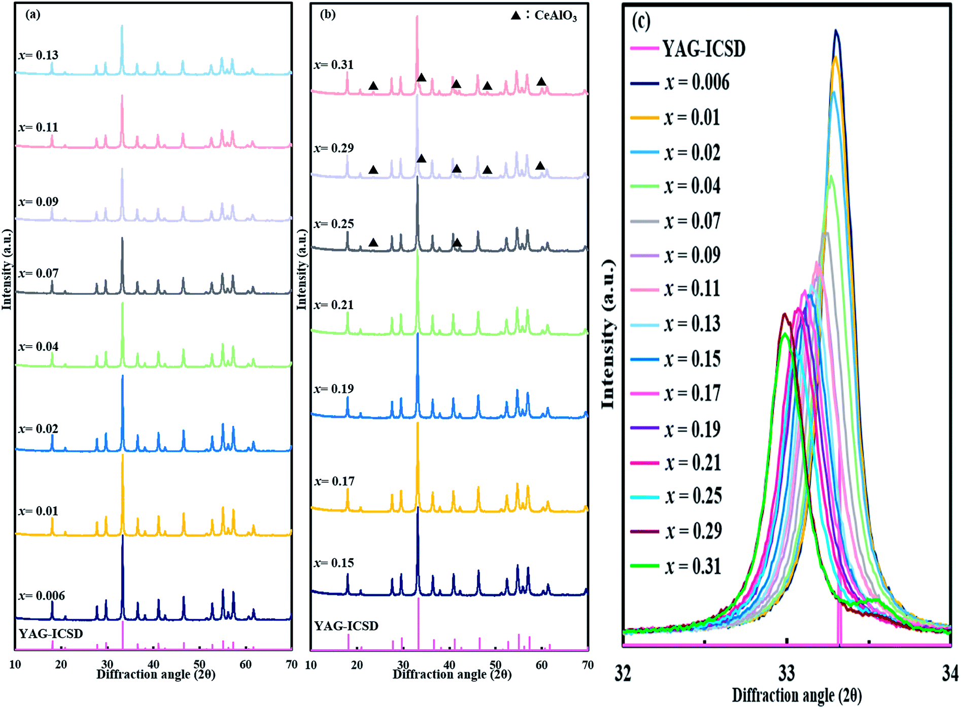
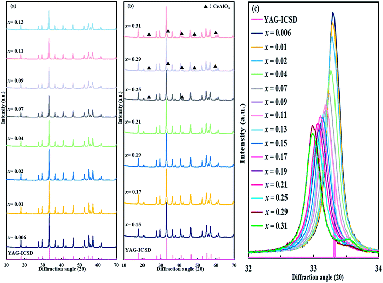
XRD patterns of (Y1−xCex)3Al5O12 (x = 0.006–0.31) are shown in Fig. 1(a) and (b). Only YAG:Ce phase exists in the samples at x = 0.006–0.21. Diffraction peaks for CeAlO3 (2θ = 23.5°, 33.5°, 41.3°, 48.0°, and 59.8°) are slightly observed at x = 0.25, and become evident with x ≥ 0.29, therefore it is not pure YAG phase at x = 0.25–0.31. To date, the boundary of formation of single-phase YAG:Ce garnet crystal is x = ∼0.09–0.12, and the highest x value reported is 0.12. Above this value, CeO2 crystals are usually segregated. The significantly high x value for single-phase (Y1−xCex)3Al5O12 observed herein is different from the previous studies. Magnified 420 diffraction lines (2θ ∼33°) are shown in Fig. 1(c). The position of diffraction line shifts toward a low angle with an increase in Ce3+ doping concentration. The shifting of diffraction line is not observed from x = 0.29 to x = 0.31. This implies that the substitution of Y site by Ce occurs, leading to the expansion of lattice up to x = 0.29. Fig. 2 illustrates the results of the Rietveld refinement for (Y1−xCex)3Al5O12 (x = 0.006, 0.17 and 0.21). The crystallographic data and initial structural model were obtained from Y3Al5O12.32 All of the observed XRD patterns of (Y1−xCex)3Al5O12 (x = 0.006, 0.17 and 0.21) were well fitted with the calculated patterns, thereby confirming the phase purity. Despite the high Ce content (x = 0.21), the results in Fig. 2 (c) indicate that the crystal phase is pure YAG:Ce. The structural parameters estimated from the Rietveld refinements are listed in Table 1. The lattice parameter of x = 0.21 is greater than that of x = 0.006. A substitution of Y with Ce occurs the cell expands, thereby resulting in an increase in the lattice parameter. This is consistent with the phenomenon of the 420 diffraction peak shifting toward a low angle.
 |
| | Fig. 1 (a and b) XRD patterns of (Y1−xCex)3Al5O12 crystals and (c) magnified XRD patterns between diffraction angles of 32° and 34°. | |
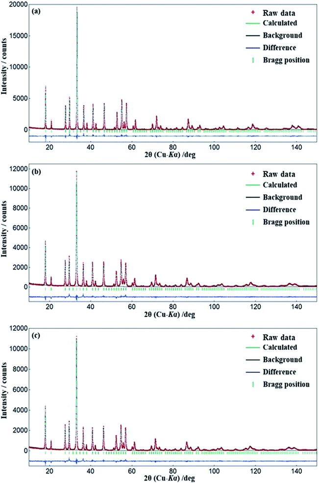 |
| | Fig. 2 Observed (+) and calculated (solid lines) XRD patterns of (Y1−xCex)3Al5O12, (a) x = 0.006; (b) x = 0.17; (c) x = 0.21 after the completion of Rietveld refinements. The vertical bars below the background level indicate the calculated positions of Kα1 and Kα2 components of the Bragg peaks. The curve at the bottom of the plots represents the difference between the observed and calculated intensities (Yiobs − Yicalc). | |
Table 1 Refined structure parameters and crystallographic data of (Y1−xCex)3Al5O12 (x = 0.006, 0.17 and 0.21)
| Chemical formula |
(Y0.994Ce0.006)3Al5O12 |
(Y0.83Ce0.17)3Al5O12 |
(Y0.79Ce0.21)3Al5O12 |
| Crystal system |
Cubic |
Cubic |
Cubic |
| Space group |
Ia![[3 with combining macron]](https://www.rsc.org/images/entities/char_0033_0304.gif) d d |
Iad |
Iad |
| Lattice parameter (Å) |
a = 12.0168(2) |
a = 12.0893(4) |
a = 12.1034(4) |
| Z Value |
8 |
8 |
8 |
| Rwp (%) |
8.017 |
8.209 |
8.172 |
| RB (%) |
l.681 |
2.039 |
2.191 |
| S |
1.408 |
1.309 |
1.266 |
| Atom |
Site |
x |
y |
z |
g |
Biso (Å2) |
| x = 0.006 |
| Y, Ce |
24c |
1/8 |
0 |
1/4 |
1.0 |
0.407(9) |
| Al1 |
16a |
0 |
0 |
0 |
1.0 |
0.275(14) |
| Al2 |
24d |
3/8 |
0 |
1/4 |
1.0 |
0.275(14) |
| O |
96h |
0.10133(11) |
0.20070(12) |
0.28146(10) |
1.0 |
0.28(3) |
|
| x = 0.17 |
| Y, Ce |
24c |
1/8 |
0 |
1/4 |
1.0 |
0.627(14) |
| Al1 |
16a |
0 |
0 |
0 |
1.0 |
0.33(2) |
| Al2 |
24d |
3/8 |
0 |
1/4 |
1.0 |
0.33(2) |
| O |
96h |
0.10236(13) |
0.20124(15) |
0.28206(12) |
1.0 |
0.37(4) |
|
| x = 0.21 |
| Y, Ce |
24c |
1/8 |
0 |
1/4 |
1.0 |
0.425(14) |
| Al1 |
16a |
0 |
0 |
0 |
1.0 |
0.17(2) |
| Al2 |
24d |
3/8 |
0 |
1/4 |
1.0 |
0.17(2) |
| O |
96h |
0.10228(14) |
0.20173(16) |
0.28225(13) |
1.0 |
0.25(4) |
The microstructures of the samples were analyzed by HRTEM (Fig. 3). As observed in Fig. 3(a) and (b), the size of the nanoparticles is 30–40 nm. In Fig. 3(c) and (d), lattice fringes are clearly observed. EDS analysis was performed at a few spots and it was confirmed that atomic ratio of Y:Al:Ce:O was mostly the same with composition ratio (Fig. 3(e) and (f)). The observed C and Cu are from the grid mesh. No impurity is detected in the sample.
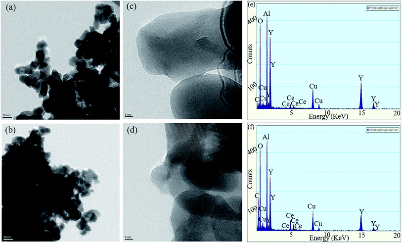 |
| | Fig. 3 (a) TEM image, and (c) HRTEM photograph of (Y1−xCex)3Al5O12 (x = 0.07); (b) TEM image, and (d) HRTEM photograph of YAG:Ce (x = 0.21); (e) EDS patterns of YAG:Ce at x = 0.07 and (f) x = 0.21. | |
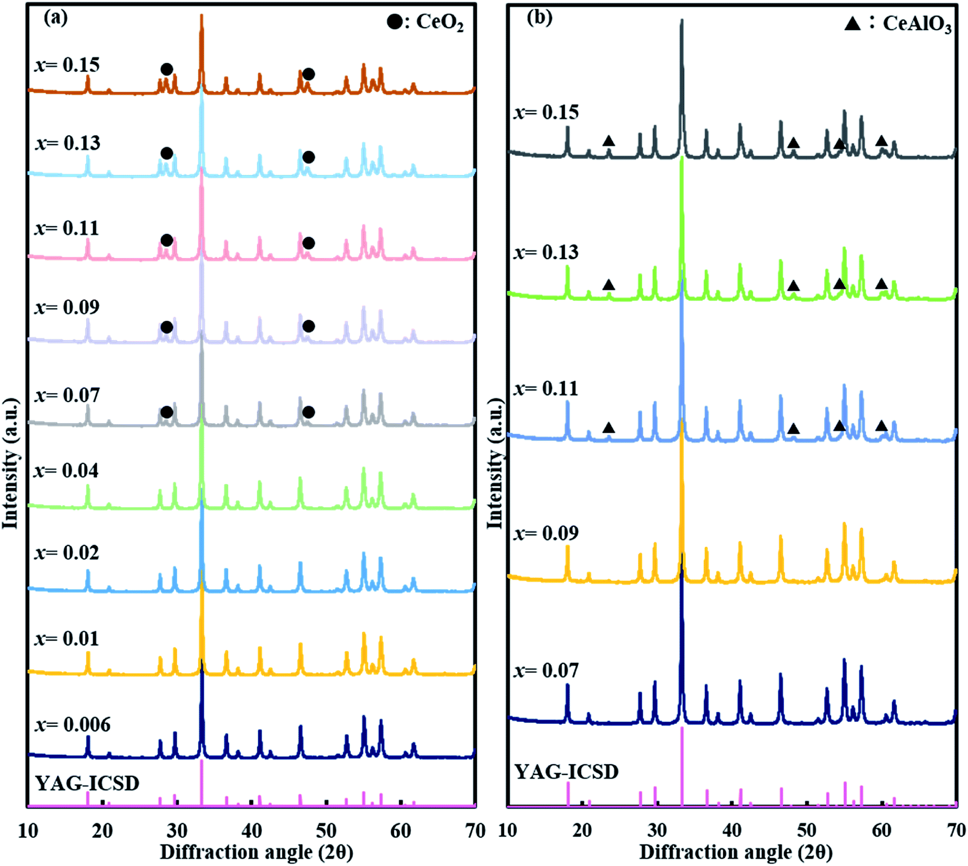
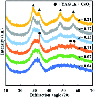
XRD and TEM results indicate that Ce is incorporated up to x = 0.21 in the single YAG:Ce crystal when two-step sintering is adopted. It was hypothesized that the incorporation of such a high content of Ce in YAG crystal was caused by the low-temperature annealing (1st step) because most of the prior studies adopted one-step sintering above 1000 °C in the preparation of YAG:Ce crystal. Hence, the samples were prepared without low-temperature annealing. Fig. 4(a) and (b) show the XRD data for ref-O and ref-R. Diffraction peaks for CeO2 are observed with x ≥ 0.07 in ref-O, while those for CeAlO3 (2θ = 23.5°,48.0°, and 59.8°) are observed with x ≥ 0.11 in ref-R. Thus, the incorporation of a high content of Ce is not observed without low-temperature annealing. Therefore, it is concluded that heat treatment at low temperature is essential to achieve a high Ce concentration in (Y1−xCex)3Al5O12.
 |
| | Fig. 4 XRD patterns of (a) ref-O and (b) ref-R. | |
3.2 Structure of (Y1−xCex)3Al5O12 precursor
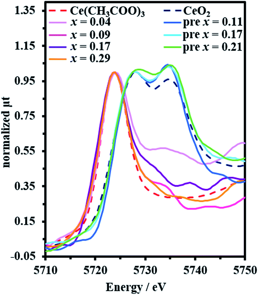
After clarifying that low-temperature annealing (1st step) was a key process to achieve a high content of Ce in YAG crystal, the valence state of Ce and structure of the precursor sample heat-treated at low temperature were investigated to elucidate the incorporation mechanism of high Ce content in YAG garnet structure. Fig. 5 displays CeLIII XANES spectra of (Y1−xCex)3Al5O12 at x = 0.04, 0.09, 0.17, and 0.29 and the precursor at x = 0.11, 0.17, and 0.21 together with those of Ce(CH3COO)3 and CeO2. The peak at 5724 eV corresponds to Ce3+, and the double peaks at 5728 eV and 5735 eV correspond to Ce4+.33 It is clearly observed that Ce exits as Ce3+ in (Y1−xCex)3Al5O12 crystals, whereas almost all Ce is in Ce4+ state in the precursor. Prior investigations of the precursor of YAG:Ce prepared by co-precipitation or sputtering33,34 show that Ce3+ is oxidized to Ce4+ when it is annealed at 600–800 °C. The oxidation of Ce by low-temperature annealing observed herein is consistent with the previously reported results.
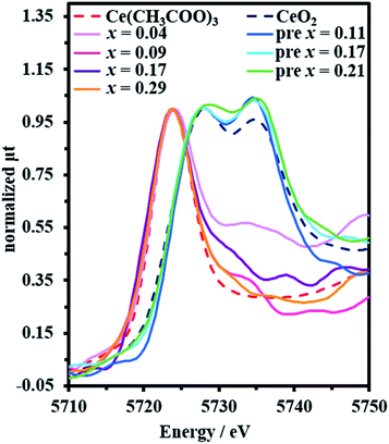 |
| | Fig. 5 Ce L3-edge XANES spectra of (Y1−xCex)3Al5O12 crystal and the precursor. CeO2 and Ce(CH3COO)3 were used as reference samples. | |
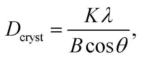
Fig. 6 shows the TEM images of the precursor samples for x = 0.04, 0.11, and 0.21. At x = 0.04, the domain with lattice fringes is not observed, which implies that the sample is mostly amorphous. In contrast, a nanocrystal domain as large as 3 nm exits showing lattice fringes at x = 0.11 and 0.21. Based on the EDS analysis, the crystal phase is composed of Y, Ce, and Al, but the difference in compositions is not clearly observed. XRD patterns of the precursor of (Y1−xCex)3Al5O12 prepared by sintering at 650 °C and 750 °C in air are shown in Fig. 7. Except for a small diffraction peak observed at x = 0.11, only broad diffraction lines are observed. An interesting feature in the figure is that the shapes of the diffraction lines significantly change with x ≥ 0.13, and four major broad diffraction peaks centered at 29°, 33°, 48°, and 57° are observed. To identify the origin of these four peaks, XRD patterns in Fig. 7 were compared with those of crystals likely to be formed in the Y2O3–CeO2–Al2O3 system such as YAG, YAlO3 (YAP), CeAlO3, Y4Al2O9 (YAM)35 and CeO2. The positions of the diffraction lines mostly coincide with those of the CeO2 crystal. The crystallite size of the crystalline phase, Dcryst, is estimated using Scherrer's equation,36
| |
 | (1) |
where
λ is the X-ray wavelength, and
B and
θ are the width and angle of the 220 diffraction line. Here, constant
K is used as 0.9.
Dcryst is thus calculated as 2.9 nm, which is similar to the crystal size observed by TEM. As the polymerized complex method is believed to form a homogeneous precursor at atomic level, it appears unlikely that CeO
2 nanocrystals are formed at low temperature. However, the phase separation of CeO
2 from the amorphous Ce–Y–Al–O phase can occur in low-temperature annealing, leading to the formation of nanocrystals.
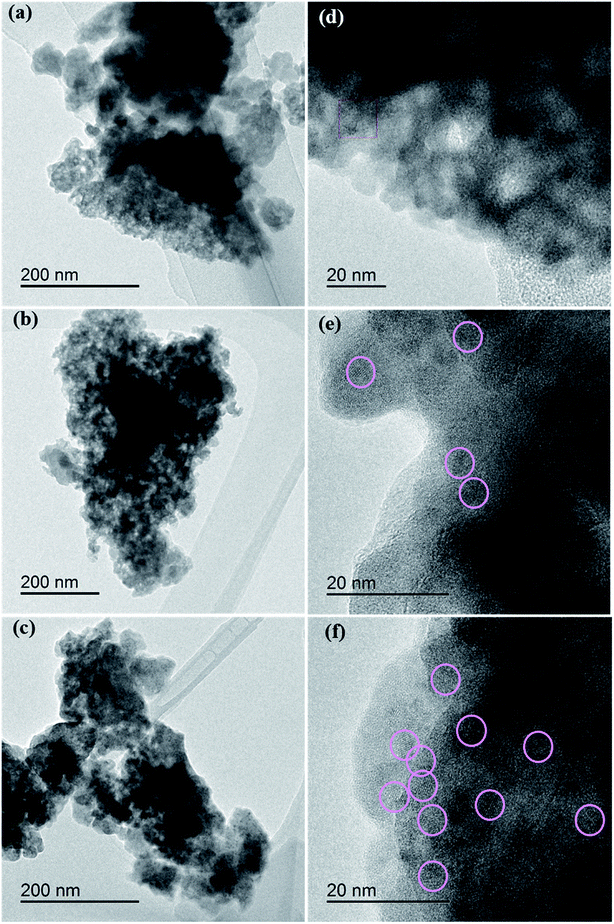 |
| | Fig. 6 TEM images of (Y1−xCex)3Al5O12 crystals. (a and d) x = 0.04, (b and e) x = 0.11, (c and f) x = 0.21. | |
 |
| | Fig. 7 XRD spectrum of the precursor of (Y1−xCex)3Al5O12. | |
In the conventional synthesis of YAG:Ce, Y2O3 progressively reacts with Al2O3 to form YAM, YAP, and YAG. As the ionic radius of Ce3+ (1.143 Å, coordination number = 8) is significantly larger than that of Y3+ (1.019 Å, coordination number = 8),37 only a small fraction of Y can be substituted by Ce. In contrast, in the synthesis described in this study, CeO2 nano-domain is first formed in Y–Al–O amorphous phase with low-temperature annealing. With successive high-temperature sintering at 1080 °C, Ce–O nano-domains becomes highly oxygen defective because of the reduction of Ce4+ to Ce3+. Y3+ existing in the boundary between CeO2 crystal and amorphous phase reacts with the Ce–O framework and finally forms YAG:Ce crystals. This specific reaction, which occurs at low temperatures, may enable the incorporation of high Ce contents.
3.3 Photoluminescent properties of crystals
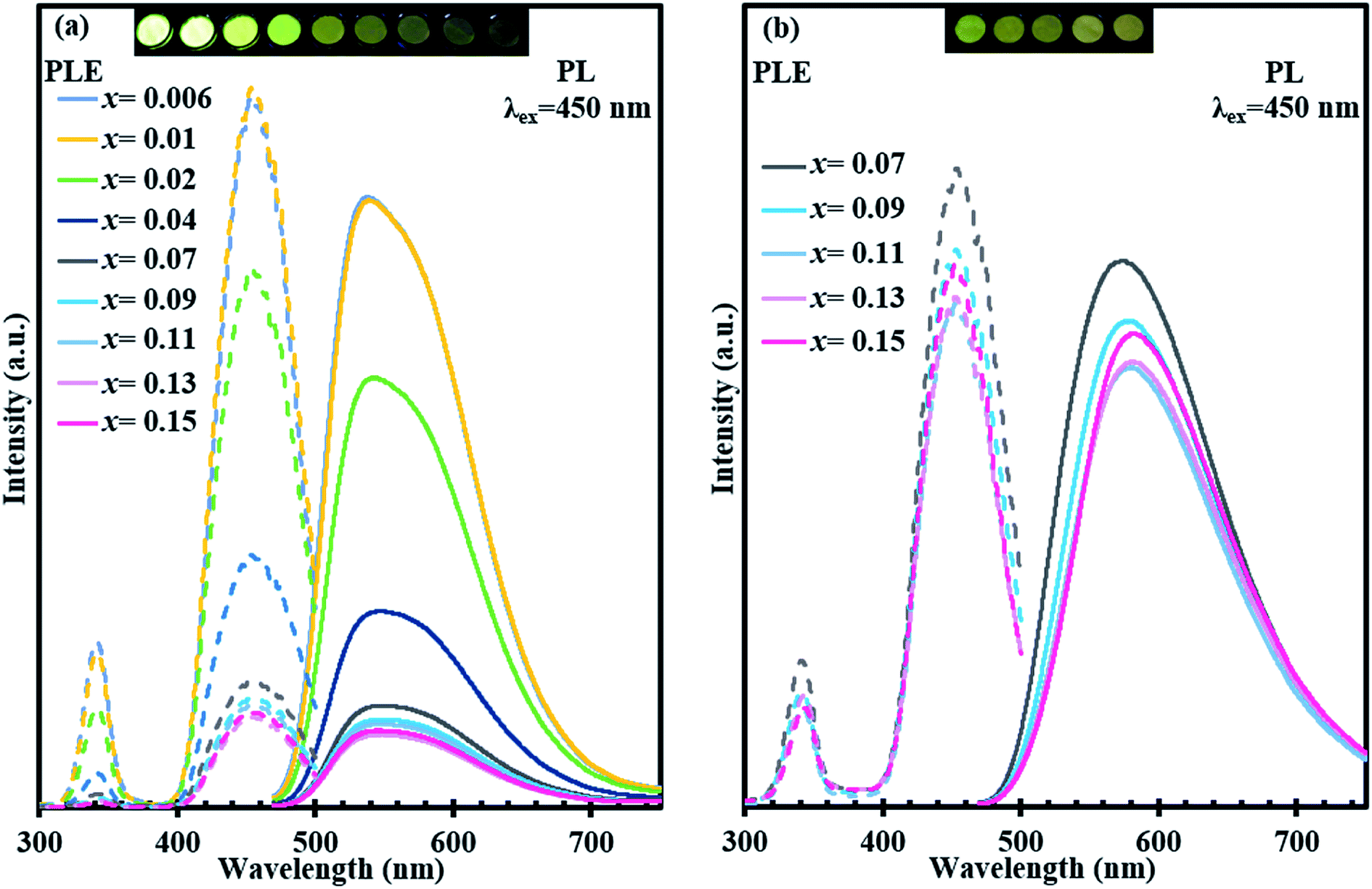
Fig. 8 shows the excitation and emission spectra for single phase (Y1−xCex)3Al5O12 (x = 0.006–0.21) together with a photograph of samples under UV irradiation (365 nm). With an increase in Ce3+ concentration from x = 0.006 to x = 0.21, the emission peak of Ce3+ shows a remarkably large red shift from 538.4 nm to 606.2 nm with excitation at 450 nm. Intensity of emission increases with an increase in Ce content from x = 0.006 to x = 0.07 but decreases with further increase in Ce content, probably due to concentration quenching. Excitation bands observed at 340 and 450 nm correspond to 4f–5d2 and 4f–5d1 transitions.10 Notably, the excitation bands at 340 and 450 nm do not show any changes in positions despite the massive red shift of emission. Diffuse reflection spectra of (Y1−xCex)3Al5O12 are shown in Fig. 9. Absorptions at approximately 355 and 460 nm correspond to 4f–5d2 and 4f–5d1 transitions. Positions of these two absorption bands do not vary significantly, which is consistent with the behavior of excitation bands in photoluminescent spectra.
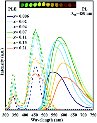 |
| | Fig. 8 Excitation and emission spectra, and the photographs of (Y1−xCex)3Al5O12 at 365 nm excitation. From left to right: x = 0.006, 0.01, 0.02, 0.04, 0.07, 0.09, 0.11, 0.13, 0.15, 0.17, 0.19 and 0.21. | |
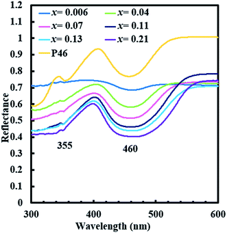 |
| | Fig. 9 Diffuse reflectance spectra of (Y1−xCex)3Al5O12 crystals. | |
The massive red shift of emission is not observed for the samples prepared without low-temperature annealing (ref-O and ref-R) as shown in Fig. 10. The emission peak of ref-O varies slightly from 538 nm to 549 nm. For ref-R, intensity and position of wavelength changes only slightly with increasing x. These results combined with XRD data indicate that low-temperature annealing causes the incorporation of high content of Ce in YAG, resulting in a massive red shift.
 |
| | Fig. 10 Excitation and emission spectra, and the photographs of (Y1−xCex)3Al5O12 (365 nm excitation). (a) Ref-O sample and (b) ref-R sample. | |
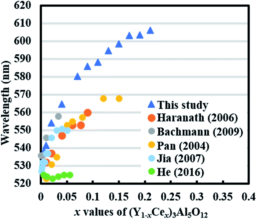
Fig. 11 includes a comparison of the relationship between the emission peak and Ce content (x) in (Y1−xCex)3Al5O12 with that of Y-substituted YAG:Ce reported till date.25–29 Notably, (Y1−xCex)3Al5O12 in this study shows a remarkably large red shift, which is significantly larger than that observed in cation-substituted YAG:Ce reported previously. The emission peak of (Y1−xREx)3Al5O12 (RE = Lu, Tb, Gd, and La) is within the 530–570 nm range. Even in the case of double substitution in YAG:Ce by Mg2+–Si4+, the longest emission is up to 598 nm.
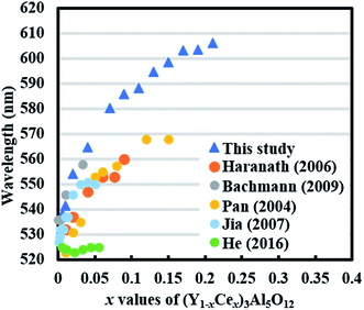 |
| | Fig. 11 Emission peaks of (Y1−xCex)3Al5O12 in relation to x. The values are acquired from literature reports.25–29 Ce concentration is described in a few different ways in literature. Data included here is converted to represent the description for (Y1−xCex)3Al5O12. | |
Fig. 12 shows the CIE chromaticity coordinates of (Y1−xCex)3Al5O12 prepared by two-step sintering. Compared with those for commercial YAG:Ce (P46) (0.428, 0.545), the CIE color chromaticity coordinates of (Y1−xCex)3Al5O12 change from (0.415, 0.549) at x = 0.006 to (0.563, 0.434) at x = 0.21, clearly tuned from green to orange-red region. The maximum internal quantum efficiency was 34% at x = 0.04. As x increased, the efficiency gradually decreased and reached approximately 14% at x = 0.21. The efficiency is not high probably because the small size of particle as large as 30 nm. The internal quantum efficiency of YAG:Ce nanoparticle powder reported so far was 18–38%.38,39
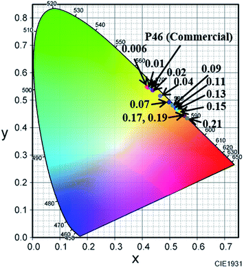 |
| | Fig. 12 CIE chromaticity coordinates of (Y1−xCex)3Al5O12 crystals. | |
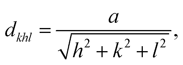
Finally, a possible mechanism for the large red shift is discussed. Although the mechanism of red shift in YAG:Ce is not fully understood, the shift in emission of Ce3+ during luminescence is generally explained by the lowering of 5d energy level in Ce3+ through centroid shift, crystal field splitting, and additional Stokes shift (Fig. 13(a)).11 The crystal field in cubic site induces the splitting of 5d energy level into two levels separated by 10Dq, where Dq is the strength of crystal field which is inversely proportional to the cation-ligand distance in classical point charge model. The crystal field strength is also strongly altered by the distortion of cubic symmetry in cation site leading to an additional splitting of the degenerate lower energy levels into two levels, d1 and d2. This additional ligand field effect is believed to be the reason for the unique long-wavelength emission of Ce3+ in YAG crystal. The energy difference between d1 and d2 (Δ12) is typically used to estimate this crystal field strength.18,40 In an attempt to understand the reason for the occurrence of a massive red shift, the Stokes shift and crystal field strength (Δ12) in (Y1−xCex)3Al5O12 is plotted against the lattice constant in Fig. 13(b) together with the values for (Y0.98−xGdx)3Al5O12:Ce0.06 reported by Shi et al.41. Here, lattice spacing, dkhl, is calculated from the hkl reflection using the equation,
where the 420 diffraction peak (2
θ ∼33.3°) is used for calculation. The lattice constant increases from 12.024 Å to 12.105 Å and 12.008 Å to 12.106 Å for (Y
1−xCe
x)
3Al
5O
12 and (Y
0.98−xGd
x)
3Al
5O
12, respectively. Despite the large lattice expansion,
Δ12 does not change significantly in (Y
1−xCe
x)
3Al
5O
12, while a gradual increase is observed in (Y
0.98−xGd
x)
3Al
5O
12:Ce
0.06. In contrast, the observed Stokes shift in (Y
1−xCe
x)
3Al
5O
12 is much larger than that in (Y
0.98−xGd
x)
3Al
5O
12. Notably, the Stokes shift determined from the difference of emission and excitation peak is not accurate because the position of emission can also shift to a large wavelength by re-excitation from the emission. However, it is speculated that the re-excitation does not have a dominant effect on the massive red shift because the overlap energy between excitation and emission is within 3–4% in the entire range of
x, which is very small to cause a considerable red shift.
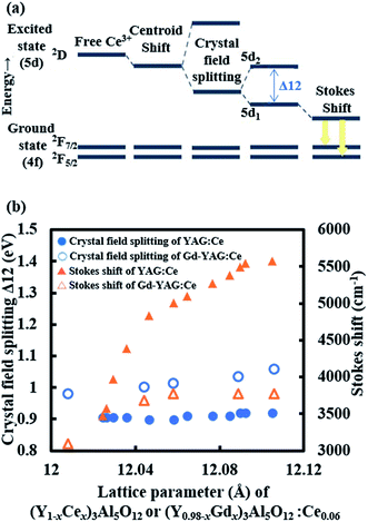 |
| | Fig. 13 (a) Energy level structure of Ce3+. (b) Crystal field splitting and Stokes shift of (Y1−xCex)3Al5O12 in relation to the lattice constant. The value for (Y0.98Gdx)3Al5O12:Ce0.06 is calculated from the data reported by Shi et al.41 Ce concentration is described in a few different ways in literature. Data included here is converted to represent the description for (Y1−xCex)3Al5O12. | |
Although the large Stokes shift is not frequently observed, it occurs in some materials.34,42 For instance, Pan et al. reported the Stokes shift of up to 4456 cm−1 in MgY2Al4SiO12:Ce3+40 while that for YAG:Ce is 3221 cm−1. They emphasized the importance of anisotropy around Ce3+ from the neighboring Mg2+ ions in the dodecahedral site. Using the configuration coordinate model, it was explained that the large Stokes shift was induced by a large equilibrium between the excited and ground state due to anisotropy. As described in the previous section, it is speculated that a CeO2 framework with a size of a few nanometers is initially formed due to low temperature annealing, and Y3+ enters this framework to form Y3Al5O12:Ce. In this case, it is possible that the spatial distribution of the Ce substituting the Y site is spatially inhomogeneous. Such inhomogeneous Ce distribution can induce local anisotropy around Ce3+, which can induce a large Stokes shift as in the case of Mg2+–Si4+-doping. However, a detailed analysis of X-ray and neutron diffraction data is needed to confirm the existence of the nano-level elemental distribution.43 In addition, another possible mechanism such as red shift by the defect due to carbon44 should be considered. These studies are currently in progress.
4. Conclusion
(Y1−xCex)3Al5O12 crystal with high Ce content (x = 0.006–0.21) was successfully prepared by a polymerized complex method via a two-step heating process for the first time. Low temperature annealing (650–750 °C) was essential to obtain (Y1−xCex)3Al5O12 (x ≥ 0.11). The precursor formed by annealing was in amorphous state with x < 0.11, while CeO2 nanocrystals with sizes up to 3 nm were formed in the amorphous material with x ≥ 0.11. The emission peak in (Y1−xCex)3Al5O12 (x = 0.006–0.21) shifted from 538.4 to 606.2 nm, exhibiting orange-red emission. Despite the large lattice expansion of host crystal, crystal field splitting (Δ12) did not show a significant increase. Hence, the large red shift could not be explained by the change in crystal field splitting, but instead by the Stokes shift. This study shows that a new optical property can be discovered in a well-known crystal. Future studies will focus on the detailed analysis of the crystal structure and dynamic process of electrons.
Conflicts of interest
There are no conflicts of interest to declare.
Acknowledgements
I would like to thank T. Uchida for technical assistance with TEM.
References
- X. Piao, T. Horikawa, H. Hanzawa and K. Machida, Chem. Lett., 2006, 35, 334–335 CrossRef CAS.
- R. J. Xie, N. Hirosaki, T. Suehiro, F. F. Xu and M. Mitomo, Chem. Mater., 2006, 18, 5578–5583 CrossRef CAS.
- H. A. Höppe, H. Lutz, P. Morys, W. Schnick and A. Seilmeier, J. Phys. Chem. Solids, 2000, 61, 2001–2006 CrossRef.
- Y. Q. Li, J. E. J. van Steen, J. W. H. van Krevel, G. Botty, A. C. A. Delsing, F. J. DiSalvo, G. de With and H. T. Hintzen, J. Alloys Compd., 2006, 417, 273–279 CrossRef CAS.
- K. Uheda, N. Hirosaki, Y. Yamamoto, A. Naito, T. Nakajima and H. Yamamoto, Electrochem. Solid-State Lett., 2006, 9, H22 CrossRef CAS.
- J. Li, T. Watanabe, N. Sakamoto, W. Hiroshi, T. Setoyama and M. Yoshimura, Chem. Mater., 2008, 20, 2095–2107 CrossRef CAS.
- Y. Sato, H. Kato, M. Kobayashi, T. Masaki, D. H. Yoon and M. Kakihana, Angew. Chem., Int. Ed., 2014, 53, 7756–7759 CrossRef CAS PubMed.
- J. Qiao, L. Ning, M. Molokeev, Y.-C. Chuang, Q. Zhang, K. Poeppelmeier and Z. Xia, Angew. Chem., Int. Ed., 2019, 58, 11521–11526 CrossRef CAS PubMed.
- T. Hasegawa, S. W. Kim, T. Ueda, T. Ishigaki, K. Uematsu, H. Takaba, K. Toda and M. Sato, J. Mater. Chem. C, 2017, 5, 9472–9478 RSC.
- G. Li, Y. Tian, Y. Zhao and J. Lin, Chem. Soc. Rev., 2015, 44, 8688–8713 RSC.
- Z. Xia and A. Meijerink, Chem. Soc. Rev., 2017, 46, 275–299 RSC.
- V. Tucureanu, A. Matei and A. M. Avram, Opto-Electron. Rev., 2015, 23, 239–251 CAS.
- M. Zhang, B. Li, Y. Yang, S. Chen, X. He, F. Zhao and Q. Zeng, J. Phys. D: Appl. Phys., 2016, 49, 415101 CrossRef.
- K. Li, G. Shucai, H. Guangyan and Z. Jilin, J. Rare Earths, 2007, 25, 692–696 CrossRef.
- Q. Meng, Y. Liu, Y. Fu, Y. Zu and Z. Zhou, J. Mol. Struct., 2018, 1151, 112–116 CrossRef CAS.
- H. S. Jang, W. Bin Im, D. C. Lee, D. Y. Jeon and S. S. Kim, J. Lumin., 2007, 126, 371–377 CrossRef CAS.
- Y. X. Pan, W. Wang, G. K. Liu, S. Skanthakumar, R. A. Rosenberg, X. Z. Guo and K. K. Li, J. Alloys Compd., 2009, 488, 638–642 CrossRef CAS.
- L. Chen, X. Chen, F. Liu, H. Chen, H. Wang, E. Zhao, Y. Jiang, T. S. Chan, C. H. Wang, W. Zhang, Y. Wang and S. Chen, Sci. Rep., 2015, 5, 1–17 CAS.
- Q. Shao, H. Li, Y. Dong, J. Jiang, C. Liang and J. He, J. Alloys Compd., 2010, 498, 199–202 CrossRef CAS.
- V. A. Chernyshev and A. V. Serdtsev, Opt. Spectrosc., 2018, 125, 646–654 CrossRef CAS.
- A. Katelnikovas, T. Bareika, P. Vitta, T. Jüstel, H. Winkler, A. Kareiva, A. Zukauskas and G. Tamulaitis, Opt. Mater., 2010, 32, 1261–1265 CrossRef CAS.
- C. He, H. Ji, Z. Huang, T. Wang, X. Zhang, Y. Liu, M. Fang, X. Wu, J. Zhang and X. Min, J. Phys. Chem. C, 2018, 122, 15659–15665 CrossRef CAS.
- Q. Du, S. Feng, H. Qin, H. Hua, H. Ding, L. Jia, Z. Zhang, J. Jiang and H. Jiang, J. Mater. Chem. C, 2018, 6, 12200–12205 RSC.
- A. Katelnikovas, H. Bettentrup, D. Uhlich, S. Sakirzanovas, T. Jüstel and A. Kareiva, J. Lumin., 2009, 129, 1356–1361 CrossRef CAS.
- V. Bachmann, C. Ronda and A. Meijerink, Chem. Mater., 2009, 21(10), 2077–2084 CrossRef CAS.
- Y. Pan, M. Wu and Q. Su, J. Phys. Chem. Solids, 2004, 65, 845–850 CrossRef CAS.
- D. Haranath, H. Chander, P. Sharma and S. Singh, Appl. Phys. Lett., 2006, 89, 2006–2008 Search PubMed.
- D. Jia, Y. Wang, X. Guo, K. Li, Y. K. Zou and W. Jia, J. Electrochem. Soc., 2006, 154, J1 CrossRef.
- X. He, X. Liu, R. Li, B. Yang, K. Yu, M. Zeng and R. Yu, Sci. Rep., 2016, 6, 1–11 CrossRef PubMed.
- M. Kakihana, J. Ceram. Soc. Jpn., 2009, 117, 857–862 CrossRef CAS.
- F. Izumi and K. Momma, Solid State Phenom., 2007, 130, 15–20 CAS.
- A. Nakatsuka, A. Yoshiasa and T. Yamanaka, Acta Crystallogr., Sect. B: Struct. Sci., 1999, 55, 266–272 CrossRef PubMed.
- H. Okura, T. Murakawa, Y. Miyamoto, T. Honma and K. Ohmi, Jpn. J. Appl. Phys., 2012, 51, 062602 Search PubMed.
- B. Wang, H. Qi, H. Han, Z. Song, J. Chen and J. Shao, Opt. Mater. Express, 2016, 6, 155 CrossRef CAS.
- R. Lampe, S. Kawelke, J. Mitternacht, V. Turova and T. Blumenstein, Opto-Electron. Rev., 2015, 23, 60–65 Search PubMed.
- A. L. Patterson, Phys. Rev., 1939, 56, 978 CrossRef CAS.
- R. D. Shannon, Acta Crystallogr., Sect. A: Cryst. Phys., Diffr., Theor. Gen. Crystallogr., 1976, 32, 751–767 CrossRef.
- T. Isobe, ECS J. Solid State Sci. Technol., 2013, 2, R3012–R3017 CrossRef CAS.
- R. Kasuya, T. Isobe, H. Kuma and J. Katano, J. Phys. Chem. B, 2005, 109, 22126–22130 CrossRef CAS PubMed.
- Z. Pan, W. Li, Y. Xu, Q. Hu and Y. Zheng, RSC Adv., 2016, 6, 20458–20466 RSC.
- H. Shi, C. Zhu, J. Huang, J. Chen, D. Chen, W. Wang, F. Wang, Y. Cao and X. Yuan, Opt. Mater. Express, 2014, 4, 649 CrossRef.
- Y. Luo, C. K. Hau, Y. Y. Yeung, K. L. Wong, K. K. Shiu and P. A. Tanner, Sci. Rep., 2018, 8, 4–11 CrossRef PubMed.
- M. Coduri, M. Scavini, M. Allieta, M. Brunelli and C. Ferrero, Chem. Mater., 2013, 25, 4278–4289 CrossRef CAS.
- Y. Zheng, W. Zhuang, X. Xing, R. Liu, Y. Li, Y. Liu, Y. Hu, X. Chen, L. Chen and X. Ma, J. Rare Earths, 2018, 36, 1239–1244 CrossRef CAS.
|
| This journal is © The Royal Society of Chemistry 2020 |
Click here to see how this site uses Cookies. View our privacy policy here. 
 Open Access Article
 This Open Access Article is licensed under a Creative Commons Attribution-Non Commercial 3.0 Unported Licence
 *a,
Kenji Shinozaki
*a,
Kenji Shinozaki