
 Open Access Article
 This Open Access Article is licensed under a Creative Commons Attribution-Non Commercial 3.0 Unported Licence
UV-cured nanocomposite coating for surface charging mitigation and breakdown strength enhancement: exploring the combination of surface topographical structure and perfluorooctyl chain†
Chao Wang ,
Wen-Dong Li,
Zhi-Hui Jiang,
Xiong Yang,
Guang-Yu Sun and
Guan-Jun Zhang*
,
Wen-Dong Li,
Zhi-Hui Jiang,
Xiong Yang,
Guang-Yu Sun and
Guan-Jun Zhang*
State Key Laboratory of Electrical Insulation and Power Equipment, School of Electrical Engineering, Xi'an Jiaotong University, Xi'an 710049, China. E-mail: gjzhang@xjtu.edu.cn
First published on 24th April 2020
Abstract
A facile method using a nanocomposite coating is proposed to suppress surface charge accumulation and enhance the surface breakdown strength of polymeric insulating materials like epoxy resin, by covering a thin 1,1,2,2-tetrahydroperfluorodecyltrimethoxysilane modified alumina (Al2O3) flake/UV curable resin nanocomposite coating. Due to the peculiar characteristics of perfluorooctyl chains at the microscale and the intricate topographical structure of morphology at the mesoscale, the coating exhibits enhanced water/oil repellence, surface charge accumulation resistance, and flashover withstanding capability. It is found that increasing the content of modified Al2O3 is conducive to decreasing the surface free energy of the specimens, rendering them superhydrophobic. Experimental tests in air show that the presence of nanoparticles generates numerous carrier traps at the surface layer, contributing to a much faster charge decay rate. Furthermore, impulse flashover voltage tests under vacuum show a >100% improvement of surface electrical strength. Further experimental results reveal that lower secondary electron emission yield remarkably alleviates the surface charging phenomenon, thus relieving electric field distortion caused by hetero-charges. We envision that such a multifunctional strategy for surface discharge mitigation is efficient, adaptable and easy to scale up, and thereby exhibits great prospects for applications in electronics and electrical power systems.
1. Introduction
Complex service environments subject polymeric insulating materials to a variety of hazards concurrently. Apart from mechanical and thermal stresses, surface discharge could lead to insulation failure, incurring catastrophic consequences to various devices like spacecraft,1 pulsed power equipment,2 power delivery equipment,3,4 etc. Fig. 1 (left). This phenomenon poses a formidable challenge with respect to compact designs and higher operating voltage level demands in insulation systems. Many theories have revealed that the build-up surface charges under the actual operating environment incline to aggravate field distortion and cause surface discharge at lower voltages, which could further deteriorate the insulation performance. Fig. 1 (middle) illustrates the possible charge behaviors (generation and dissipation) occurring at the dielectric surface. Apparently, the source of surface charge is multitudinous: e.g. triboelectrification,5 field emission,6 secondary electron emission (SEE),6,7 near-surface gas ionization,8 etc. Particularly, SEE and gas ionization usually are considered as the main reasons for charge accumulation in vacuum/insulator and gas/insulator system, respectively. Meanwhile, many factors like humidity,9,10 surface conductivity,10 and neutralization contribute to the dissipation of accumulated charge. Surface charges also dissipate when migrating towards the material bulk. In the past decades, numerous studies have been dedicated to efficient suppression of surface charging from two main aspects: i.e. inhibiting generation and accelerating dissipation, summarized in Fig. 1 (right). On the one hand, for an insulation system, decreasing the maximum electric strength and controlling field direction by geometry design,11 dielectric graded material,12 or nonlinear fillers13 can reduce charge generation caused by field emission or gas ionization, and facilitate surface charge carriers decay under the modulated electric field, respectively. On the other hand, strategies aimed at material surface are comparatively more universal and adaptable. Previous researches indicated that surface physical states and chemical component are key factors that affect the generation and migration of charge carriers, Fig. 1 (upper-right). Intricate micro or macro topography created by plasma etching,14 mechanical grooving15 or polishing,16 and laser shaping,17 are used to set barriers for discharge development and improve conductivity to alleviate charge accumulation. Chemical functionalization methods including direct or plasma assisted fluorination,18,19 radical elimination,10 and nano fillers addition,20 can suppress charge generation and accelerate dissipation as well.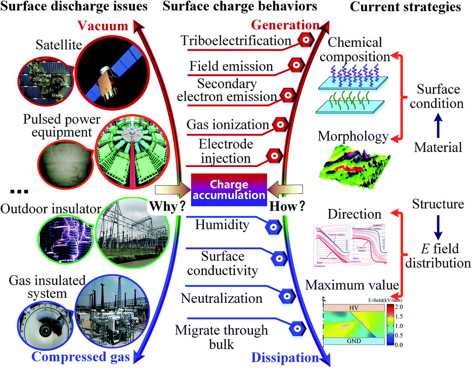 | ||
| Fig. 1 A list of the practical applications, fundamental mechanisms for surface charge generation or dissipation, and general strategies for surface electric strength enhancement of vacuum/solid or gas/solid interface. | ||
All these methods, however, aim at a single objective (i.e. inhibiting surface charging from mono source or accelerating charge dissipation by mono way), resulting in poor universality and applicability due to the complexity of charging processes. For instance, methods to inhibit charge generated by triboelectrification has been systematically studied from the mechanism to application, and has been comprehensively reviewed in ref. 21 and 22. Nonetheless, some other processes in Fig. 1 are also accompanied by the consecutive formation of surface charges. Moreover, unfavorable conditions like dust deposition and icing may lead to insulation failure as well.23 It is also notable that a recent advancement in material design geared toward integration of multiple functions into one material.24,25 This constructive strategy is universal, robust, and adaptable for dealing with real application scenarios. Is there a multifunctional strategy for effective suppressing surface charge accumulation, and improving surface electrical strength of insulator? To this end, a nanocomposite coating with excellent hydrophobicity, high surface electrical strength, fast charge decay rate, and low secondary electron emission yield (SEEY) is prepared by UV curing process. Compared to thermal curing technique, photopolymerization is efficient (fast curing speed) and energy-saving (operating at room temperature), and therefore has been widely used in various fields related to surface engineering.26,27 Here, fluorocarbon modified Al2O3 flakes were blended with UV curable resin, synthesizing a new type of composite which could be cured under UV light illumination. Comparing with other nanoparticles, nano-Al2O3 in the form flakes has larger specific surface area, which benefits the fabrication of this multifunctional coating. Finally, the interplays among surface topographical structure at mesoscale and perfluorooctyl chain at microscale, surface charge behavior and surface breakdown strength in vacuum and atmospheric environment were further analyzed. It is believed that this efficient, adaptable and multifunctional approach overcomes the challenges of conventional surface treatment techniques and shows huge potential to be widely used in a variety of energy and electronic applications.
2. Experimental section
2.1. Preparation of nanocomposite coating
Initially, nano Al2O3 was prepared by a liquid method (detailed preparation technique and characterization results are shown in the ESI Section A†). On the one hand, the prepared flakes with large specific surface area contribute to the surface modification and morphology alternation. On the other hand, flakes can form abundant inorganic/organic interfaces to enhance charge dissipation and to protect insulator surfaces from hot electron bombardment.28 In our previous researches, we found that fluorinated chains with alkyls structure can decrease surface free energy and enhance surface electrical strength.29,30 Hence, silane coupling agent (1,1,2,2-tetrahydroperfluorodecyltrimethoxysilane, FAS17) was grafted at the nanoparticles surface to serve as fluorination layer. Also, to guarantee strong bonding strength between fillers and matrix, inorganic fillers are usually modified by chemical groups that can react with the matrix. With these considerations, silane coupling agents including FAS17 and γ-methacryloxypropyl trimethoxy silane (KH570) were grafted at the surface of Al2O3 particles. Then the modified nanoparticles were loaded to the UV curable resin to prepare nanocomposite. Finally, these photo-curable nanocomposites were sprayed to the surface of epoxy resin (a commonly used material in electronic/electrical systems), and then cured in a customized UV-curing chamber to obtain a thin film on the insulator's surface. More details about the preparation process are shown in ESI Section B.†2.2. Characterization of surface morphology, chemical composition, and wettability
Morphologies of nanoparticles before and after surface modification were observed by transmission electron microscope (TEM, JEOL JEM2100F). Crystalline structure of the inorganic fillers was characterized by XRD (Bruker D8-Advance, Karlsruhe) with Cu-Kα radiation. Scanning range of diffraction angle (2θ) was from 10° to 70° stepped by 0.02° per second. Fourier transform infrared spectra (FTIR, Thermo Fisher Nicolet iN10) was recorded to characterize surface groups of the nanoparticles. XPS (Thermo Fisher ESCALAB Xi+) were measured to confirm the segregation of fluorinated chains. The surface morphology of the coating was characterized by field emission scanning electron microscope (SEM, ZEISS GeminiSEM 500). In addition, the cross-sectional morphology after liquid nitrogen freezing was characterized by SEM (VE-9800S). Laser scanning confocal microscope (LSCM, Olympus LEXT OLS4000) was applied to characterize 3D morphology of the coating. Further, the measurement of average roughness (Ra) was performed on a contact type instrument (MarSurf M 300C, Germany). To test for water/oil repellence, ∼1 μL deionized water and diiodo-methane droplets were dispensed toward the coating surface. Then the static contact angle was recorded by optical contact angle measuring device (KRUSS DSA100S).2.3. Surface conductivity, charge decay, secondary electron emission, charge distribution and electrical strength characterization
Surface conductivity measurements were conducted by a pico-ampere meter (6517B, Keithley) with 8009 standard fixture. The measurements of SEEY were performed in a high vacuum chamber (<5 × 10⁻⁴ Pa) including an electron gun (EGL-2022, Kimball), producing electron beam with energy from 50 eV to 5 keV. Electrical strengths in air and vacuum were characterized by a self-designed system, which can generate impulse voltage up to 80 kV. Surface potential distribution after the impulses was measured by an electrostatic voltmeter (Trek341B) connected by a vibrating Kelvin probe (Trek 3455ET), with the probe scanning in a region of 48 × 30 mm. In the same way, surface charge decay at a single point was also recorded by the electrostatic voltmeter. All the experimental details about these electrical properties characterizations can be found in the ESI Section C.†3. Results and discussion
3.1. Characterization of prepared nanoparticles
Characterization results of morphologies (Fig. S1a, ESI†) from TEM show that the prepared particles have flaky structure with average size of 27.6 nm and the average thickness is about 4.3 nm (detailed statistical approach are described in the ESI Section A†). X-ray diffraction (XRD) analysis (Fig. S1c†) shows that the nanoparticles have multiple peaks at 2θ = 20, 32.7, 37.2, 39.5, 45.8, 61, and 67°, which are the typical reflections of γ-Al2O3. The crucial factor of this multifunctional coating lies in the preparation of perfluorooctyl chain grafted nano Al2O3 flakes (Fig. 2a). The covalent linkage of silane coupling agents including FAS17 and KH570 to Al2O3 flakes were confirmed by TEM observations and Fourier-transform infrared (FT-IR) spectra. The inset of Fig. S1b† shows an amorphous layer with a thickness of about 3 nm outside the Al2O3 nanoparticles. Intuitively, silane coupling agents have been successfully coated onto the surface of the nanoparticles. The FT-IR result of KH570 + FAS17@Al2O3 in Fig. S1d† shows many peaks comparing with that of pristine Al2O3. Apart from the obvious peak around 3400 cm−1 (–OH), additional peaks appearing at 2945, 2850, 1723, 1640, 1247, 1205, and 1095 cm−1 should attribute to –CH3, –CH2, –C![[double bond, length as m-dash]](https://www.rsc.org/images/entities/char_e001.gif) O, –CC, –CF3, –CF2, and –C–O–C, respectively.
O, –CC, –CF3, –CF2, and –C–O–C, respectively.
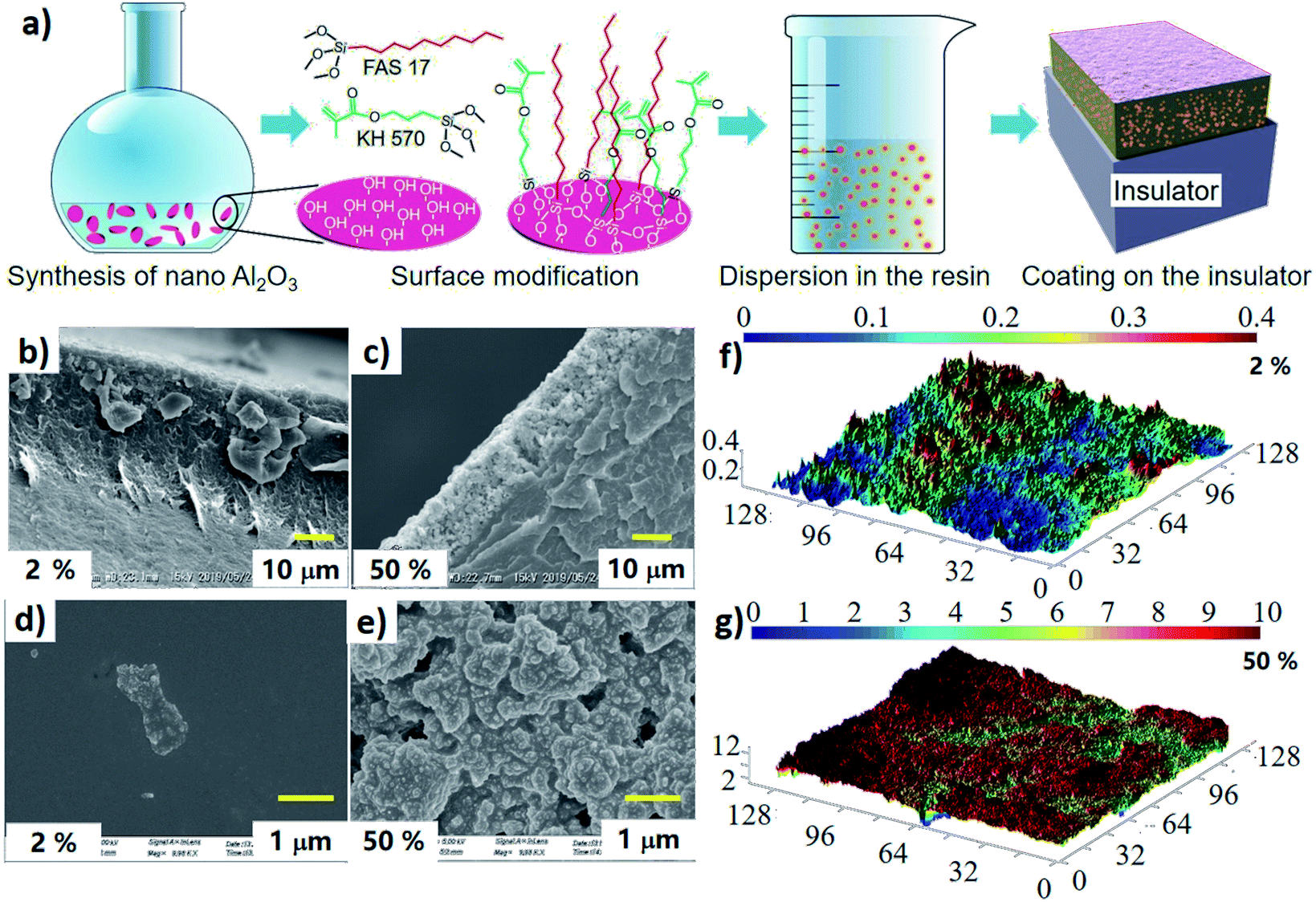 | ||
| Fig. 2 Experimental designs and featured morphologies of the UV curable composite coating. (a) Synthetic scheme of UV-cured composite coating. (b) and (c) Cross-sectional SEM, (d) and (e) superficial SEM, (f) and (g) 3D morphology images of UV-F-2% and UV-F-50%, respectively. | ||
3.2. Characterization of UV-cured resin/modified Al2O3 composite
O) in Fig. 3b, additional peaks in Fig. 3c at 291.7 and 293.8 eV are attributed to the –CF2 and –CF3 groups, respectively. O 1s spectrum of UV-F-2% (Fig. S3a†) shows two peaks at 532 eV (C–O) and 533.7 eV (CO), while no peak is observed in F 1s spectrum (Fig. S3b†). In contrast, O 1s spectrum of UV-F-50% (Fig. S3c†) shows two new peaks at 531.1, and 532.97 eV, which should be contributed to Al2O3 fillers and Si–O groups in silane coupling agents, respectively. By the same token, strong peaks appear in F 1s spectrum because of the presence of C–F chains (Fig. S3d†). FT-IR spectra of the coating were measured at attenuated total reflection (ATR) mode (Fig. S3e†). The decrease of peaks strength in 1728.8 cm−1 (–CO), 1467.5 and 1452.1 cm−1 (–CH2 and –CH3), 1200.5 cm−1 (OC–O–C) and 1112.7 cm−1 (–C–O–C), and the presence of –CF2 peak at 1095 cm−1 indicate that the amount of modified nanoparticles in the UV-cured composite layer is increased. Photographs of water and diiodo-methane droplets on the coating surface are presented in Fig. 3d and e, respectively. Interestingly, liquid contact angle is not in a linear relationship with the fillers loading ratio in the preparation of the coating layer. This should be ascribed to the difference of roughness shown in Table S3.† At very low loading ratio (2%), surface wettability is mainly determined by surface chemical composition since the amount of nanoparticles is small. In this case, hydrophobic surface benefits from the chemical groups with low surface energy. With the increase of loading ratios, the distance among nanoparticles further decreases, droplets tend to contact directly with the surface when the air escapes out of the roughness, transiting into a Wenzel wetting state (smaller contact angle is observed in this stage). When fillers loading ratio further increases (≥30%), nanoscale roughness is generated. A thin layer of air is trapped between the solid surface and the liquid, transiting into a Cassie state.31,32 In this case, an increase in the amount of nano fillers employed in the initial mixture produces surfaces with higher contact angle. As shown in Fig. 3f, UV-F-50% has very low surface energy of 1.90 mN m−1 as compared with the 14.45 mN m−1 of UV-F-2, and the maximum water contact angle achieve up to 153.64°. This superhydrophobic function has the potential to protect dielectric from moisture absorption and icing or frosting in some special circumstances.33
 | ||
| Fig. 3 (a) XPS scans of UV-F-2% and UV-F-50%. C 1s envelopes of (b) UV-F-2% and (c) UV-F-50% with prominent C–F2 and C–F3 peaks, indicating the presence of FAS 17 at the surface. (d) and (e), respectively, photographs of water and diiodo-methane droplets on the coating surface at different loading ratios. (f) Values of contact angle and surface free energy of the coating. | ||
3.3. Electrical performance
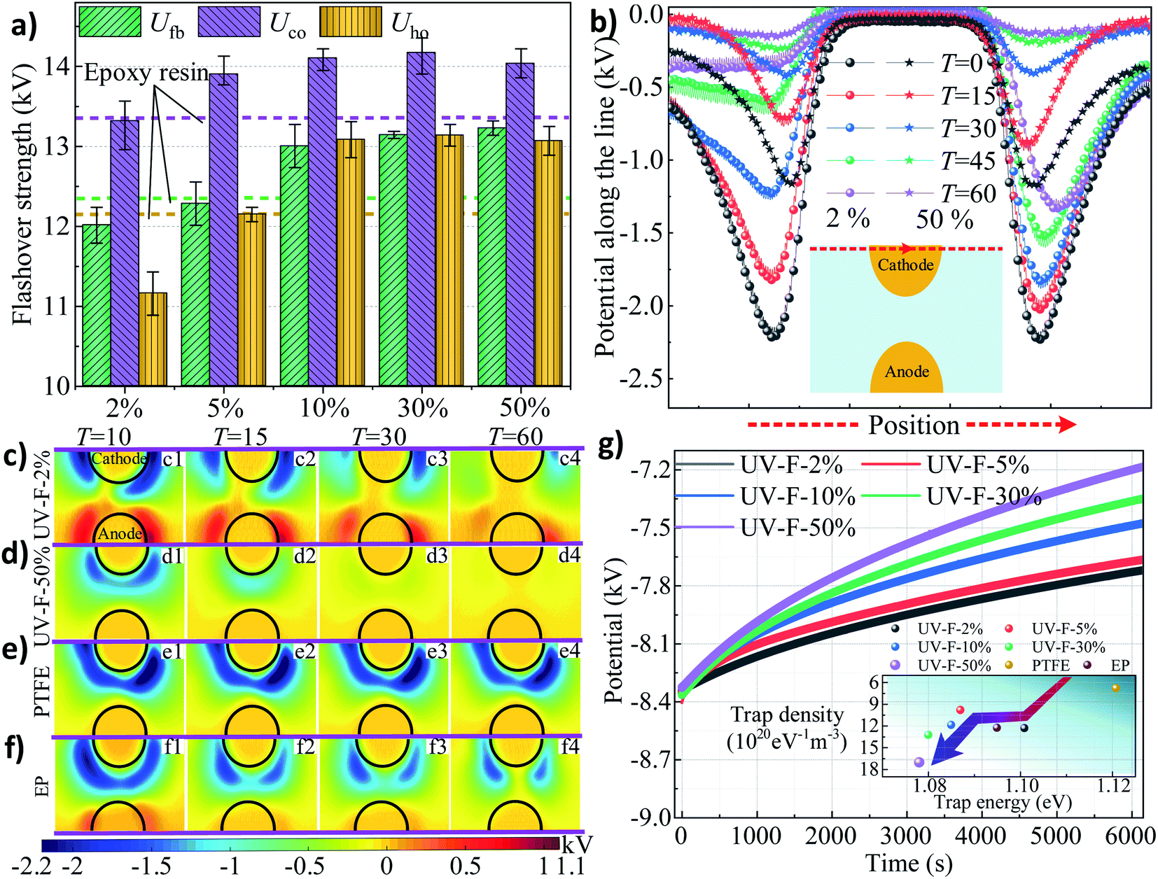 | ||
| Fig. 4 Experimental results in atmosphere. (a) Impulse flashover voltages of specimens with different fillers content. (b) Variations of surface potential of UV-F-2% and UV-F-50% along a line with time. The inset is the illustration of electrode/insulator layout, and the position of the line. Overall potential distribution of (c) UV-F-2%, (d) UV-F-50%, (e) PTFE, and (f) EP within different decay time. The length of decay time after the pulses is denoted as T. (g) Surface potential decay profiles for UV-F series during surface traps measurement process. The inset displays the comparisons of trap peak position among UV-F-x%, PTFE, and EP. Higher trap density and lower trap energy level means faster surface charge dissipation. | ||
Isothermal surface potential decay (ISPD) of UV-F series measured by electrometer are shown in Fig. 4g. Not surprisingly, with the increase of fillers content, surface charge decay rate also increases rapidly. According to the surface electron trap information calculated by ISPD method,35 shallower traps are introduced to the surface by coating this nanocomposite layer (the inset of Fig. 4g). The trap energy peak shifts from original 1.11 eV (UV-F-2%) to 1.07 eV (UV-F-50%) and the trap density increases from 12.35 × 10²⁰ to 17.32 × 10²⁰ eV−1 m−3. Note also that the PTFE shows deepest trap level and the minimum traps density. It should be the intrinsic physical mechanisms that account for the differences of surface charge decay rate. The fast charge decay property of the coating is supposed to be another useful function for the insulator, which can keep desirable voltage in targets and protect them from charge accumulation especially in dc voltage conditions.
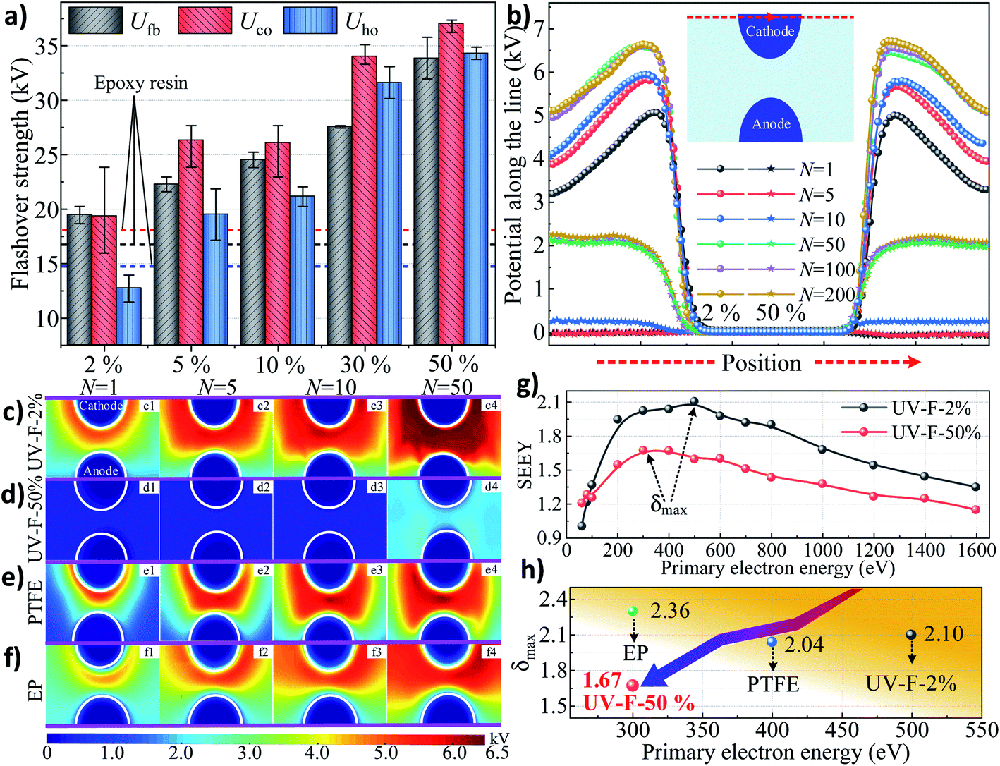 | ||
| Fig. 5 Experimental results in vacuum. (a) Impulse flashover voltages of specimens with different fillers content. Potential distribution of (b) variations of surface potential of UV-F-2% and UV-F-50% along a line with pulse time. The inset is the illustration of electrode/insulator layout, and the position of the line. Overall potential distribution of (c) UV-F-2%, (d) UV-F-50%, (e) PTFE, and (f) EP after applying −30 kV voltage with different times. The number of pulses times is denoted as N. (g) SEEY profiles of UV-F-2% and UV-F-50%. (h) The comparisons of δmax position among UV-F-2%, UV-F-50%, PTFE, and EP. Lower δmax and the corresponding primary electron energy means less surface charge accumulation. | ||
3.4. Physical model establishment and mechanism explanation
A multiscale integrated physical model is established to elaborate the interplay between the surface states of the coating layer and discharge development or the following charge migration process. A typical insulation system is shown in Fig. 6a. High voltage (HV) source generates the E field between anode and cathode at the specimen surface. At the mesoscale (μm ∼ mm), surface morphology could be altered by adding inorganic fillers, and the roughness level can be modulated from nm to μm (Fig. 6b). Regarding microscale (Å ∼ nm), the C–F chains grafted at the nanoparticles' surface form a fluorinated layer with a thickness of 3 nm (Fig. 6c). These surface characteristics at different scale have strong correlation with the surface charge behaviors. | ||
| Fig. 6 Physical model for the nanocomposite coating. (a) Insulation system with a cathode and anode bridging along the insulator surface. (b) Surface topological structure at mesoscale. (c) Surface molecular structure at microscale. (d) Physical model for describing charge behavior in atmosphere. (e) Physical model for describing charge behavior in vacuum. | ||
In gas atmosphere, gas ionization accounts for the sources of surface charge. It needs to be mentioned that negative charges are accumulated at the surface because more electrons than ions enter the solid boundary during plasma sheath formation (Fig. 4), thus only electron dynamics is discussed here, and the positive charge transport is not considered in the present work. Previous researches indicate that hopping transport mechanism is well-accepted for explaining electrical behavior in insulating polymers and understanding charge transport in disordered semiconductors and amorphous solids.37 These theories assume that the motion of electrons through the insulator is governed by availability of localized states. Topological and chemical disorder can break the symmetry of the ordered system, forming localized states which concentrate in band tails.38 In the case of UV-F-2% (Fig. 6d), once charges are deposited on the surface, few energy traps can be provided for charge transportation since the amount of Al2O3 flake is limited. For UV-F-50%, physical defects like corners, pits, and pores can serve as shallow traps. Additionally, chemical disorder caused by C–F chains can be considered as relatively deeper traps. These localized states provide numerous paths for electron jumping, resulting in faster charge decay rate comparing with that of UV-F-2%.
In vacuum, surface charging mechanism is totally different. As shown in Fig. 6e, the surface of UV-F-2% is very smooth, electrons emitted from the cathode are sufficiently accelerated by the applied E field before reaching insulator. Hence, incident electrons can easily penetrate into the interior of the composites due to the relatively high energy, and only few of them are reflected at the surface by inelastic backscattering and elastic reflection (IBS & ER). Thereafter, SEE avalanche contributes to electron loss for the material, leaving abundant holes on the surface. These positive charges provide recombination center for the subsequent incident electrons. Finally, a self-sustained SEE situation is reached where SEEY is equal to 1. In contrast, rougher surface of UV-F-50% decreases the electron collision mean free path before impacting the insulator surface. Free electrons gain limited energy from the E field, hence, hindering the development of SEE avalanche to some extent. Also, barriers set by the intricate morphology can induce multiple IBS & ER process at each interface for the newly created secondary electrons, which also contribute to the absorption attenuation of incident electrons. At microscale, factors like surface molecular chain also play a role for charge transport. C–F chains can act as electron traps to absorb electrons due to the strong electron affinity of fluorine atoms, thereby reducing the number of secondary electrons. To sum up, it is because of the synergistic effect of surface morphology and fluorinated chains that leading to different SEE efficiencies and surface potential under the same level of excited voltage.
3.5. Comparison of flashover mitigation strategies reported in recent literature with our work
To fully exhibit the great advantages of this research in the industrial applications, a comparison is carried out between the flashover mitigation strategies reported in recent literatures and experimental works in this paper. Flashover voltage (Uho) improvement ratio in vacuum, and other factors of direct fluorination,39 Mechanical polishing,40 plasma etching,14 laser grooving41 are compared and the corresponding results are summarized in Fig. 7. Note that the other factors consideration means a comprehensive evaluation including cost, process adaptability and functional diversity.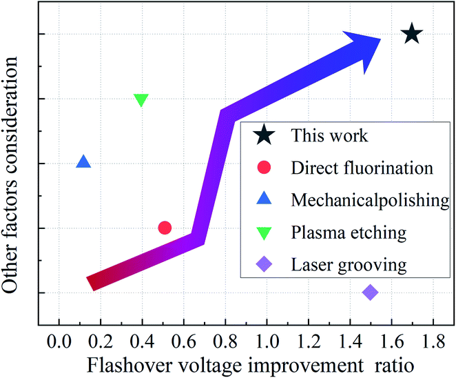 | ||
| Fig. 7 Comparison of different methods reported in recent literature with our work. | ||
4. Conclusions
To summarize, a multifunctional strategy for the surface flashover mitigation of polymer insulating material is presented by the combination of surface topographical structure and perfluorooctyl chain. Low surface energy, low SEE, fast charge decay rate coating was fabricated through UV curing technique. UV curable resin with internal phase fractions as high as 50 wt% of fluorosilane modified alumina nanoparticles forms a thin film on the surface of insulator upon light radiation. The main findings could be listed as follows:(1) Because of the micro/nano hierarchical structure generated by the nano Al2O3 flakes and the fluorinated chains grafted at Al2O3 surface, the coating exhibits the highest superhydrophobicity with a contact angle of 153° and surface energy of 1.90 mN m−1.
(2) Furthermore, surface topographical features including corners, pits, and pores at the nano-/micro-scale leads to the considerable increase of shallow traps. ISPD results showed that the trap energy peak could shift from original 1.11 eV (UV-F-2%) to 1.07 eV (UV-F-50%) and the trap density increases from 12.35 × 10²⁰ to 17.32 × 10²⁰ eV−1 m−3, thereby accelerating the dissipation of surface charge in air.
(3) Additionally, the noticeable roughening of surface features and drastic enrichment of fluorinated groups synergistically suppress secondary electron emission from 2.10 to 1.67. As a result, surface charging phenomena under impulse voltage strike are suppressed and flashover voltage Uho increases from to 12.7 to 34.3 kV.
The present fabrication process features this technique efficient, and scalable, thus applicable for the high throughput preparation of more robust and reliable insulation systems without compromising the bulk characteristics.
Conflicts of interest
There are no conflicts to declare.Acknowledgements
This study was financially supported by the National Natural Science Foundation of China (Grant No. U1766218, 11775175, 51827809). We thank Dr Dongli Zhao of Guangzhou Haoda Company for the help in the preparation of nano Al2O3. Also, we appreciate the kind help from Mr Rundong Zhou in the measurement of secondary electron emission characteristics.References
- K. Toyoda, T. Okumura, S. Hosoda and M. Cho, J. Spacecr. Rockets, 2005, 42, 947–953 CrossRef.
- G. J. Zhang, G. B. Su, B. P. Song and H. B. Mu, IEEE Trans. Dielectr. Electr. Insul., 2018, 25, 2321–2339 CAS.
- A. R. Verma and B. S. Reddy, Eng. Failure Anal., 2019, 95, 214–225 CrossRef CAS.
- B. Qi, C. Gao, C. Li and J. Xiong, Int. J. Elec. Power., 2019, 105, 514–520 CrossRef.
- J. Wu, X. L. Wang, H. Q. Li, F. Wang, W. X. Yang and Y. Q. Hu, Nano Energy, 2018, 48, 607–616 CrossRef CAS.
- G. Y. Sun, B. H. Guo, B. P. Song, G. Q. Su, H. B. Mu and G. J. Zhang, Phys. Plasmas, 2018, 25, 9 Search PubMed.
- J. Z. Gleizer, Y. Krasik, U. Dai and J. Leopold, IEEE Trans. Dielectr. Electr. Insul., 2014, 21, 2394–2404 Search PubMed.
- A. A. Neuber, M. Butcher, H. Krompholz, L. L. Hatfield and M. Kristiansen, IEEE Trans. Plasma Sci., 2000, 28, 1593–1598 CrossRef CAS.
- K. W. Biegaj, M. G. Rowland, T. M. Lukas and J. Y. Y. Heng, ACS Omega, 2017, 21, 576–1582 Search PubMed.
- H. T. Baytekin, B. Baytekin, T. M. Hermans, B. Kowalczyk and B. A. Grzybowski, Science, 2013, 341, 1368–1371 CrossRef CAS PubMed.
- J. L. Wang, B. Yue, X. G. Deng, T. Q. Liu and Z. R. Peng, IEEE Trans. Dielectr. Electr. Insul., 2018, 25, 321–329 CAS.
- W. D. Li, X. R. Li, B. H. Guo, C. Wang, Z. Liu and G. J. Zhang, IEEE Trans. Dielectr. Electr. Insul., 2019, 26, 1–9 CAS.
- C. Li, C. Lin, J. Hu, W. Liu, Q. Li, B. Zhang, S. He, Y. Yang, F. Liu and J. He, IEEE Trans. Dielectr. Electr. Insul., 2018, 25, 1238–1247 CAS.
- S. L. Chen, S. Wang, Y. B. Wang, B. H. Guo, G. Q. Li, Z. S. Chang and G. J. Zhang, Appl. Surf. Sci., 2017, 414, 107–113 CrossRef CAS.
- C. Chang, H. J. Huang, G. Z. Liu, C. H. Chen, Q. Hou, J. Y. Fang, X. X. Zhu and Y. P. Zhang, J. Appl. Phys., 2009, 105, 7 CrossRef.
- J. Y. Xue, H. Wang, J. H. Chen, K. F. Li, Y. Q. Liu, B. P. Song, J. B. Deng and G. J. Zhang, J. Appl. Phys., 2018, 124, 11 Search PubMed.
- Z. P. Yan, X. D. Liang, I. Cotton and C. Emersic, IEEE Trans. Dielectr. Electr. Insul., 2018, 25, 1095–1102 CAS.
- T. Shao, W. J. Yang, C. Zhang, Z. Niu, P. Yan and E. Schamiloglu, Appl. Phys. Lett., 2014, 105, 5 Search PubMed.
- F. Kong, C. Chang, Y. Y. Ma, C. Zhang, C. Y. Ren and T. Shao, Appl. Surf. Sci., 2018, 459, 300–308 CrossRef CAS.
- S. He, C. Lin, J. Hu, C. Li and J. He, J. Phys. D: Appl. Phys., 2018, 51, 215306 CrossRef.
- L. F. Chen, Q. F. Shi, Y. J. Sun, T. Nguyen, C. Lee and S. Soh, Adv. Mater., 2018, 30, 15 Search PubMed.
- D. J. Lacks and T. Shinbrot, Nat. Rev. Chem., 2019, 3, 465–476 CrossRef CAS.
- Y. Liu and B. X. Du, IEEE Trans. Dielectr. Electr. Insul., 2010, 17, 465–472 Search PubMed.
- Y. Zhang, C. H. Zhang, Y. Feng, T. D. Zhang, Q. G. Chen, Q. G. Chi, L. Z. Liu, G. F. Li, Y. Cui, X. Wang, Z. M. Dang and Q. Q. Lei, Nano Energy, 2019, 56, 138–150 CrossRef CAS.
- Y. Li, X. Liu, X. Nie, W. Yang, Y. Wang, R. Yu and J. Shui, Adv. Funct. Mater., 2019, 10, 1807624 CrossRef.
- X. Zhu, Z. Li, Y. Hu, H. Li, J. Yang and H. Lan, Opt. Laser Technol., 2020, 123, 105943 CrossRef.
- X. Y. Zhu, Q. Xu, H. K. Li, M. Y. Liu, Z. H. Li, K. Yang, J. W. Zhao, L. Qian, Z. L. Peng, G. M. Zhang, J. J. Yang, F. Wang, D. C. Li and H. B. Lan, Adv. Mater., 2019, 31, 9 Search PubMed.
- B. Zhang, Q. Wang, Y. Zhang, W. Gao, Y. Hou and G. Zhang, Nanoscale, 2019, 11, 18046–18051 RSC.
- C. Wang, J. Guo, W. D. Li, X. R. Li, Z. H. Jiang, B. H. Guo and G. J. Zhang, Mater. Lett., 2019, 249, 17–20 CrossRef CAS.
- C. Wang, W. D. Li, J. Guo, X. Chen, Z.-H. Jiang, X. R. Li, B. H. Guo and G. J. Zhang, Appl. Surf. Sci., 2019, 505, 144432 CrossRef.
- V. Jokinen, E. Kankuri, S. Hoshian, S. Franssila and R. H. A. Ras, Adv. Mater., 2018, 30, 10 Search PubMed.
- L. R. J. Scarratt, U. Steiner and C. Neto, Adv. Colloid Interface Sci., 2017, 246, 133–152 CrossRef CAS PubMed.
- A. Davis, Y. H. Yeong, A. Steele, I. S. Bayer and E. Loth, ACS Appl. Mater. Interfaces, 2014, 6, 9272–9279 CrossRef CAS PubMed.
- Y. Wang, D. Y. Qiang, Z. Q. Xu, G. Chen and A. Vaughan, J. Phys. D: Appl. Phys., 2018, 51, 10 Search PubMed.
- W. W. Shen, H. B. Mu, G. J. Zhang, J. B. Deng and D. M. Tu, J. Appl. Phys., 2013, 113, 083706 CrossRef.
- G. Y. Sun, B. P. Song, B. H. Guo, R. D. Zhou, S. Zhang, H. B. Mu and G. J. Zhang, J. Phys. D: Appl. Phys., 2018, 51, 295201 CrossRef.
- J. R. Dennison and J. Brunson, IEEE Trans. Plasma Sci., 2008, 36, 2246–2252 CAS.
- G. Blaise, J. Electrost., 2001, 50, 69–89 CrossRef CAS.
- R. D. Zhou, G. Y. Sun, B. P. Song, B. H. Guo, N. Yang, H. B. Mu and G. J. Zhang, J. Phys. D: Appl. Phys., 2019, 52, 375304 CrossRef CAS.
- B. H. Guo, G. Y. Sun, S. Zhang, J. Y. Xue, R. D. Zhou, B. P. Song, H. B. Mu and G. J. Zhang, J. Phys. D: Appl. Phys., 2019, 52, 215301 CrossRef CAS.
- Y. K. Huo, W. Y. Liu, C. F. Ke, C. Chang and C. H. Chen, J. Appl. Phys., 2017, 122, 115105 CrossRef.
Footnote |
| † Electronic supplementary information (ESI) available: Materials and sample preparation; materials characterization methods; FT-IR, TEM and XPS analysis results; electrical property test methods, including measurements of surface potential, trap energy, DC conductivity, surface charge distribution, and flashover voltage in vacuum and air. See DOI: 10.1039/d0ra01344g |
| This journal is © The Royal Society of Chemistry 2020 |