
 Open Access Article
 This Open Access Article is licensed under a
 Creative Commons Attribution 3.0 Unported Licence
Rapid synthesis of vertically aligned α-MoO3 nanostructures on substrates†
Sohaila Z. Noby*ab,
Ka Kan Wonga,
Ananthakumar Ramadoss c,
Stephan Sirokyd,
Matthias Hagnera,
Klaus Boldte and
Lukas Schmidt-Mende*a
c,
Stephan Sirokyd,
Matthias Hagnera,
Klaus Boldte and
Lukas Schmidt-Mende*a
aDepartment of Physics, University of Konstanz, 78457 Konstanz, Germany. E-mail: lukas.schmidt-mende@uni-konstanz.de
bNational Research Centre NRC, Department of Solid State of Physics, 12622 Cairo, Egypt
cSARP-LARPM, Central Institute of Plastic Engineering and Technology (CIPET), 751024 Bhubaneswar, India
dDepartment of Chemistry, University of Konstanz, 78457 Konstanz, Germany
eDepartment of Chemistry & Zukunftskolleg, University of Konstanz, 78457 Konstanz, Germany
First published on 24th June 2020
Abstract
We report a new procedure for large scale, reproducible and fast synthesis of polycrystalline, dense, vertically aligned α-MoO3 nanostructures on conducting (FTO) and non-conducting substrates (Si/SiO2) by using a simple, low-cost hydrothermal technique. The synthesis method consists of two steps, firstly formation of a thermally evaporated Cr/MoO3 seed layer, and secondly growth of the nanostructures in a highly acidic precursor solution. In this report, we document a growth process of vertically aligned α-MoO3 nanostructures with varying growth parameters, such as pH and precursor concentration influencing the resulting structure. Vertically aligned MoO3 nanostructures are valuable for different applications such as electrode material for organic and dye-sensitized solar cells, as a photocatalyst, and in Li-ion batteries, display devices and memory devices due to their high surface area.
1 Introduction
Over the last decade, transition metal oxides with reduced dimensionality (2D, 1D, 0D) have gained attention as a building block for various hierarchical micro and nanostructures in smart, functional materials due to their excellent physical, chemical, electrical and optical properties.1 Molybdenum trioxide (MoO3) as a wide band gap material occupies a prominent position among other transition metal oxides, owing to its distinctive properties such as 2D layered structure and not completely filled d-orbitals. MoO3 can be employed in a wide range of applications such as organic solar cells,2 Li-ion batteries where 2D layered MoO3 material is currently seen as the strongest competitor against graphene,3,4 heterogeneous catalysis,5 chemical6 and bio-sensors,7 water splitting8 and memory devices.9 MoO3 exists in three different crystal structures, orthorhombic (α-MoO3), monoclinic (β-MoO3), and hexagonal (h-MoO3). The α-MoO3 crystal structure is a thermodynamically stable layered structure with Pbnm symmetry. It consists of distorted [MoO6]6+ octahedra, which are connected in a zig–zag chain via edges along the [100] direction and linked via corners in trans position in the [001] direction, forming double layers along the [010] direction.10 h-MoO3 is formed from the same [MoO6]6+ zig–zag chains, which are linked by corners in cis position forming a tunnel structure.11The synthesis of various MoO3 nanostructures has been achieved through different methods,12 including electro-deposition,13 thermal evaporation,14 chemical vapour deposition,15 sonochemical methods,16 flame,17 aqueous solution processes,18 laser-assisted evaporation,19 and ultrasonic spray pyrolysis.20 The morphological engineering development is owing to the unique characteristics of large surface area, the small dimensions comparable to the Debye length, superior stability, and ease functionalization, which differ from the respective bulk properties.21,22 However, growing dense, vertically aligned 1D MoO3 nanostructures in a reproducible manner remains a big challenge. Vertically aligned 2D and 1D nanostructures films were found to enhance the sensitivity of gas sensing materials in comparison to a random network of 2D materials on a substrate.23–25 Recently, highly efficient, low power consuming, and long-lasting vertically aligned nanowire-based multifunctional devices have been demonstrated in different applications such as MEMS-based sensors and flexible wearable and portable safety clothes26 and multisensor chips (optical, magnetic and conductometric gas sensor).27 Vertically aligned metal oxides have been integrated into organic solar cells, which showed improved charge separation and extraction.28 The aforementioned synthesis procedures for vertically aligned 1D and 2D MoO3 rely on a range of sophisticated techniques such as using thermal evaporation at very high boat temperature of 1100 °C to prepare the structures on Si substrates,29 plasma-assisted paste sublimation on nickel coated glass,30 and also modified hotplate method at 450 °C on Au/Si substrates.31 Those methods require high temperature or are limited to certain types of substrates. Furthermore, the final product is neither highly reproducible nor does it provide a very dense structure, but only a low number of wires or flakes per unit area. The hydrothermal process is the most versatile and cheapest technique employed in nanochemistry to grow a variety of nanostructures. It has been used intensively to synthesise MoO3 nanostructures as a powder or dispersion. Additionally, the hydrothermal technique has been used to grow direct 2D and 1D structures of other metal oxides on substrates such as ZnO, TiO2 and SnO2. However, we are not aware of such synthesis directly on substrates for MoO3.
An essential goal of this work is to grow vertically aligned, densely packed MoO3 structures as films on substrates such as transparent conducting oxides (TCOs) or Si. Here, we report specifically an efficient method to produce a homogeneous and dense, vertically aligned film of two-dimensional α-MoO3 nano-blades on seeded substrates using a highly reproducible, hydrothermal method with, short reaction. The synthesis proceeds without the use of any additional organic surfactants, catalysts, or dispersing additives. Here, we studied the various parameters such as reaction time, precursor concentration, and pH value to control the growth, the morphology and phase evolution of the MoO3 nanostructure.
2 Experimental section
2.1. Chemicals
All materials included in our study have used as received and used without further purification. For the precursor solution, sodium molybdate dihydrate (99.5%, Sigma Aldrich), and hydrochloric acid (37%, VWR chemicals) were used. As evaporation sources for the seed layer molybdenum(VI) oxide powder (99.98%, Sigma Aldrich) and chrome plated tungsten rods (99.9%, Testbourne) were used.2.2. MoO3 seed layer formation/coating
Different types of substrates such as commercial fluorine-doped tin oxides (FTO) (15 Ω cm−2), p-doped Si/SiO2 wafers (SiO2 thickness: 1 μm) were cleaned using a standard procedure by sonication in acetone (5 min), isopropanol (5 min), and ethanol (15 min), followed by drying in a nitrogen flow. The cleaned substrates were treated with a UV/ozone cleaner (Ossila) for 20 min to form a polar surface to improve the adhesion of the MoO3 seed layer.32 The MoO3 seed layer was deposited on the different substrates using thermal evaporation (Tectra mini-coater) at a base pressure of <2 × 10⁻⁶ mbar with applied current and power of 15 A and 1 kW, respectively. The thickness of the film was monitored using a quartz micro-balance with a resolution of ±0.1 nm. Finally, the seed layer coated substrate was annealed at 450 °C for 1 h under ambient atmosphere.2.3. Vertically aligned of MoO3 nanostructures growth process
An aliquot of concentrated hydrochloric acid (HCl) was added dropwise to an aqueous solution of Na2MoO4·2H2O into a PTFE autoclave liner to yield a total volume of 21.5 mL. The mixed solution was stirred for at least 10 min to dissolve the precursors completely. Then, the seed layer coated substrates were placed upright into a PTFE holder and submerged in the prepared precursor solution. Finally, the PTFE autoclave liner was sealed and put into a pre-heated oven at 180 °C for 210 min. After the reaction, the autoclave was rapidly cooled down to ambient temperature in a water bath. The grown MoO3 substrates were washed with ethanol and allowed to dry under ambient conditions.2.4. Characterization
X-ray diffraction (XRD) analysis was performed with a Bruker AXS D8 Advance diffractometer employing a Bragg–Brentano geometry and Cu-Kα radiation and using a grazing incidence geometry (GIXRD). Surface imaging was done using Zeiss Cross Beam 1540XB field emission scanning electron microscope (FE-SEM) using an acceleration voltage of 5 kV. High-resolution transmission electron microscope (HR-TEM) images were obtained on a JEOL JEM-2200FS microscope operated at 200 kV. The HR-TEM samples were prepared on carbon-coated copper grids supplied by Quantifoil GmbH. The obtained nanostructures were analyzed with selected area electron diffraction (SAED), bright-field imaging, and zero-loss filtered high-resolution TEM.3 Results and discussion
A dense layer of vertically aligned MoO3 nano-blades was prepared on various substrates through a process, which consists of first depositing the seed layer, followed by hydrothermal synthesis of the MoO3 film. The whole synthesis process is schematically represented in Fig. 1.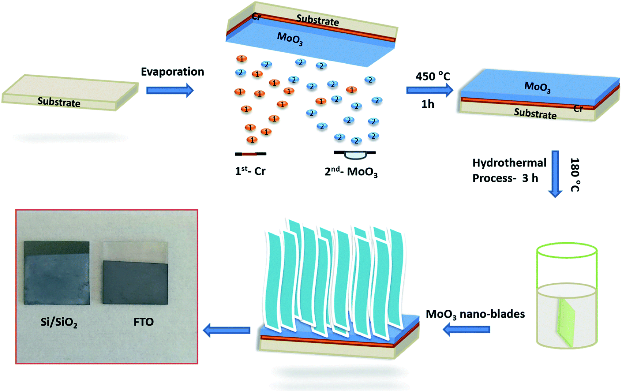 | ||
| Fig. 1 Schematic illustration of synthesis process of vertically aligned α-MoO3 nano-blades. | ||
3.1. Influence of adhesive and seed layers on the growth of vertically aligned MoO3 nano-blades
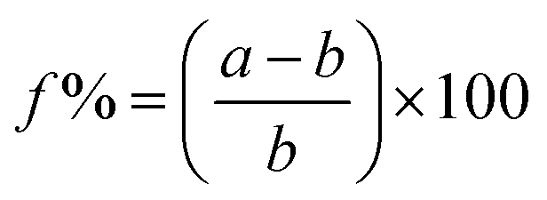
To ensure proper adhesion of the nanostructures on the substrate, a thin adhesion layer has to be deposited initially. We found that only Cr worked well as adhesion layer for the MoO3 growth.The structure and composition of the Cr layer were characterized using GIXRD at a grazing incidence angle of 0.5°. In Fig. 2, the XRD patterns of the Cr adhesive layer with thicknesses of 5, 10 and 20 nm are presented. The Cr-layer was directly exposed to an annealing process (450 °C for 1 h) to ensure the same condition, which has been applied to the complete seed layer, including the evaporated MoO3 layer on top of the Cr layer. The obtained XRD pattern revealed that the coated metallic Cr was converted to chromium oxides consisting of the two most stable chromium oxides phases: rhombohedral Cr2O3 and cubic Cr3O. Oxidation of the Cr layer can be attributed to interaction with the oxygen-rich substrate on the bottom, as well as the formation of the metal oxide layer from the top during the annealing process.33 The stoichiometry changed in favour of Cr3O in thicker adhesive layers, indicated by the increasing intensity of the (210) reflex at 44.55° as a predominant peak of Cr3O (space group Pm![[3 with combining macron]](https://www.rsc.org/images/entities/char_0033_0304.gif) n, JCPDS 01-072-0528). An earlier study has shown that this phase of Cr oxide is formed from the interaction between Cr2O3 and metallic Cr.34 In the case of thinner layers (5 nm) Cr3O cannot be detected. Cr2O3 was indicated by the (104) reflex at 33.58° (space group Rc, JCPDS 00-006-0504) and this result is consistent with previous studies, which indicate conversion of Cr to its oxides by applying heat treatment and/or exposure to an oxygen-rich atmosphere.35,36 The broad peak observed in all films centred at 21.4° (indicated by “*”) is attributed to the amorphous SiO2 substrate (JCPDS 01-086-1561).37 It was demonstrated that the chromium layer forms very strong chemical bonds to the oxidized substrate (SiO2, FTO) via an oxide transition layer.38,39 In the seminal study by Benjamin et al. reveals that the adhesion of the Cr layer on glass substrates is enhancing with the time. In particular, it affirms a better adhesion compared to nobel metals, strongly depending on the deposition condition and exposure to air.38,40 The thickness of the Cr oxide layer was found to be influenced by the temperature during oxygen exposure and saturates at 400 °C.36 Furthermore, prior studies33 have shown that using Cr as an adhesion layer for Au/dielectric and semiconductor materials on glass and oxidized substrates decreased the roughness of the Au layer, which leads to smaller and more stable nucleation centres. Best adhesion was reported for thicknesses between 1 and 30 nm. Thicker films up to 100 nm lead to stress, which causes delamination.41 Benjamin et al. showed that the Cr layer was composed of closely spaced islands with a width of 5 nm, and a height of 10 nm,38 which is consistent to our observation (see ESI, Fig. S1†). We suggest that beyond acting as an adhesion layer, the Cr oxide could also function as nucleation centres. The atomic radii of Cr and Mo are similar, which allows the adhesion layer to reduce the lattice mismatch between α-MoO3 and the substrate. The effect can be quantified by comparing the lattice misfit (f) between the exposed lattice planes according to XRD calculated through the relation: MoO3/FTO: 16%, MoO3/SiO2: 21%, Cr2O3/FTO only 6%, Cr2O3/SiO2 as little as 1%, Cr3O/FTO: 4% and Cr3O/SiO2: 9%, which are calculated through theoretical bulk values (see ESI, Table S1,† for used lattice parameters):42
n, JCPDS 01-072-0528). An earlier study has shown that this phase of Cr oxide is formed from the interaction between Cr2O3 and metallic Cr.34 In the case of thinner layers (5 nm) Cr3O cannot be detected. Cr2O3 was indicated by the (104) reflex at 33.58° (space group Rc, JCPDS 00-006-0504) and this result is consistent with previous studies, which indicate conversion of Cr to its oxides by applying heat treatment and/or exposure to an oxygen-rich atmosphere.35,36 The broad peak observed in all films centred at 21.4° (indicated by “*”) is attributed to the amorphous SiO2 substrate (JCPDS 01-086-1561).37 It was demonstrated that the chromium layer forms very strong chemical bonds to the oxidized substrate (SiO2, FTO) via an oxide transition layer.38,39 In the seminal study by Benjamin et al. reveals that the adhesion of the Cr layer on glass substrates is enhancing with the time. In particular, it affirms a better adhesion compared to nobel metals, strongly depending on the deposition condition and exposure to air.38,40 The thickness of the Cr oxide layer was found to be influenced by the temperature during oxygen exposure and saturates at 400 °C.36 Furthermore, prior studies33 have shown that using Cr as an adhesion layer for Au/dielectric and semiconductor materials on glass and oxidized substrates decreased the roughness of the Au layer, which leads to smaller and more stable nucleation centres. Best adhesion was reported for thicknesses between 1 and 30 nm. Thicker films up to 100 nm lead to stress, which causes delamination.41 Benjamin et al. showed that the Cr layer was composed of closely spaced islands with a width of 5 nm, and a height of 10 nm,38 which is consistent to our observation (see ESI, Fig. S1†). We suggest that beyond acting as an adhesion layer, the Cr oxide could also function as nucleation centres. The atomic radii of Cr and Mo are similar, which allows the adhesion layer to reduce the lattice mismatch between α-MoO3 and the substrate. The effect can be quantified by comparing the lattice misfit (f) between the exposed lattice planes according to XRD calculated through the relation: MoO3/FTO: 16%, MoO3/SiO2: 21%, Cr2O3/FTO only 6%, Cr2O3/SiO2 as little as 1%, Cr3O/FTO: 4% and Cr3O/SiO2: 9%, which are calculated through theoretical bulk values (see ESI, Table S1,† for used lattice parameters):42
 | (1) |
 | ||
| Fig. 2 GIXRD patterns of annealed chromium layer on Si/SiO2 substrates, with corresponding stick patterns of Cr2O3 (black) and Cr3O (red), respectively. The star indicates the amorphous SiO2 peak. | ||
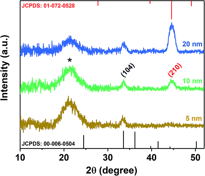
A 100 nm of the MoO3 seed layer was directly deposited onto the Cr layer, followed by annealing at 450 °C for 1 h. This leads to the formation of pure α-MoO3,43 which has been confirmed by X-ray diffraction (Fig. 3a, JCPDS – 005-0508).12 A thickness of 100 nm was found to be optimal to uniformly cover the whole substrate, which was directly reflected in the density of MoO3 growth (see ESI, Fig. S2†).
 | ||
| Fig. 3 (a) XRD spectra of the annealed seed layer and vertically aligned α-MoO3 nano-blades on FTO substrates, (b and c) FE-SEM images of vertically aligned α-MoO3 nano-blades, (d and e) HRTEM-SAED of α-MoO3 nano-blades, (f) Schematic of MoO3-nano-blades growth planes on the substrate. | ||
3.2. Growth of vertically aligned MoO3 nano-blades
Vertically aligned MoO3 nano-blades were grown directly on the pre-treated seeded substrates under hydrothermal conditions using sodium molybdate as a precursor under strongly acidic conditions. The effect of growth temperature and time on the MoO3 structure was systematically analysed by FE-SEM at different growth temperature between 100–200 °C and reaction times between 60–210 min. Prior studies have established that in strongly acidic conditions [MoO4]2− ions condensate into hydrated MoO3 via several polymolybdate intermediates.44 At elevated pressure and temperature >100 °C the product loses water of crystallisation to form α-MoO3 as can be seen in eqn (2):
 | (2) |
At optimized precursor concentration and a temperature of 180 °C, the reaction results in a dense array of aligned MoO3 nanostructures after 3 h, as shown in Fig. 3b. The XRD analysis of the nano-blades demonstrates that they crystallize in the α-MoO3 phase, the same structure as the seed layer. No reflexes of any other phase, impurity or inter-diffusion from the Cr layer could be detected (see Fig. 3a). The sharp reflexes in the diffractogram indicate that the nano-blades are highly crystalline (for the analogous reaction on Si/SiO2 substrates see ESI, Fig. S3†). Raman spectra confirmed that the material is pure, stoichiometric α-MoO3 (see ESI, Fig. S4†) The XRD pattern was found to have a preferred orientation favouring the (021) planes, which reflects the single crystalline growth along the [001] axis, in a good agreement with previously reported studies.1,12 The cross-sectional FE-SEM image (Fig. 3c) confirmed the vertical growth of MoO3 nanostructures and arrangement in rows and bundles with a flower-like structure. No by-products from the precursor decomposition appeared as shown in EDX (see ESI Fig. S3†). The individual nano-blades are ca. 10–50 nm wide, as shown by HRTEM (Fig. 3d), and consist of fragile 2D sheets that do not stack onto each other. Selected area electron diffraction (SAED, Fig. 3e) recorded perpendicular to the growth axis of the blades is attributed to [010] zone axis which supports preferential growth along the [001] direction (Fig. 3f). The anisotropic crystal growth ties well with the previous study for well-ordered MoO3 layers prepared on substrates.45,46 It suggests that the nano-blade formation occurs via a direct precipitation reaction of highly anisotropic α-MoO3.47 The nano-blades grow linearly with reaction time until the precursor is wholly consumed or the reaction is interrupted by rapid cooling, as shown in Fig. 4. It is worth mentioning that increasing the hydrothermal reaction time results in overgrowth of the fine structure (see ESI, Fig. S5†). Also, we observe weak adhesion in these overgrown samples, likely due to higher stress triggered by the increased film thickness. This constitutes a significant increase in reaction rate compared to previous studies on hydrothermal synthesis of MoO3 nanorods and fibres which give reaction times between 7 h and 7 days respectively.11,44,48–52 In our study the growth time is significantly reduced by a factor of 50 of such 2D structures.
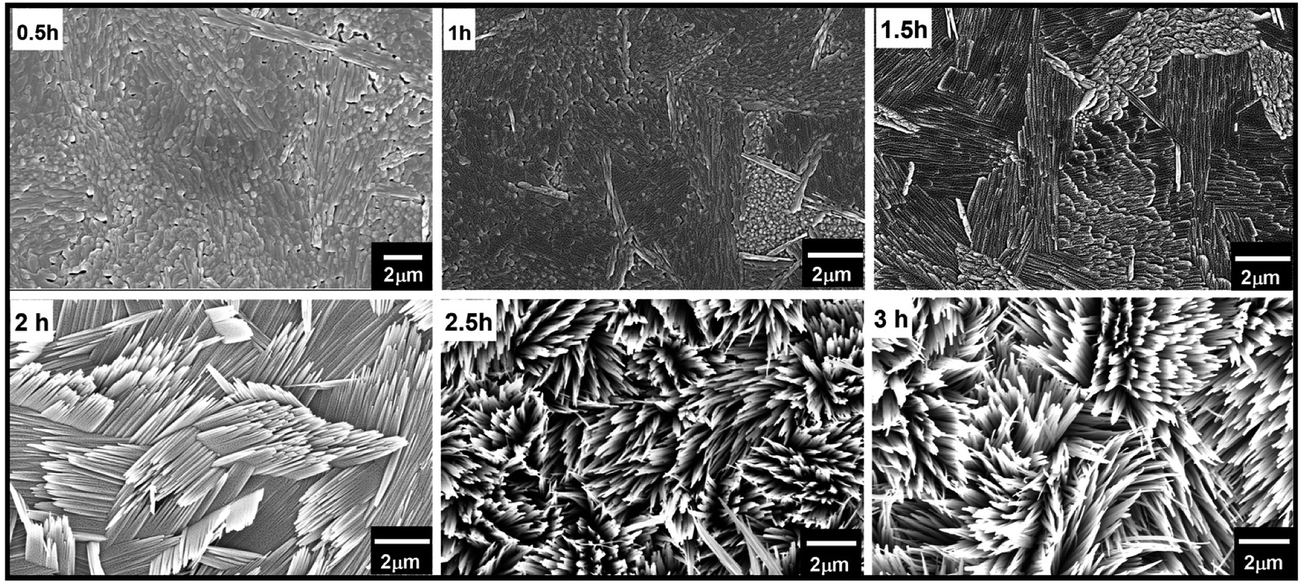 | ||
| Fig. 4 FE-SEM micrographs show the growth of vertically aligned α-MoO3 on FTO at different times during the hydrothermal reaction using 0.3 mol L−1 acid concentration and reaction temperature of 180 °C. | ||
We propose that the increasing in the growth rate is triggered by the introduction of our MoO3 seed layer, which provides direct nucleation sites for the hierarchical structure growth. Therefore, no-prior time for the formation of nucleation sites is required, allowing a direct initiation of the growth and reducing the growth times considerably (Fig. 4). Another indication for this can be found by carefully looking at the backside of the seed layer (see ESI Fig S6†). Their MoO3 crystallites can be observed. Therefore, the nucleation has already occurred before the hydrothermal reaction.
3.3. Growth mechanism of aligned MoO3 nanostructures
Hydrothermal synthesis depends on many variables factors which affect the morphology of the resulting nanostructure.53 Acid and precursor concentration and reaction time were identified to have the most substantial impact on the immediate reaction. The rate at which the acid was added to the Na2MoO4 solution to form the reaction precursor was found to be crucial for the shape control of the resulting nanostructures. Slow addition with a rate of ∼1 drop per second yielded thin blades, while a faster rate led to the formation of hexagonal monoliths with a significantly reduced surface area. This highlights the importance of precursor structure and ageing. The absolute amount of acid was used to control the length of the resulting nano-blades with different heights. The isopolymolybdate anions contain octahedral coordinated Mo(VI) ions that are connected via edges, as opposed to the tetrahedral coordinated MoO42, and thus form a fragment of the α-MoO3 target structure. By varying the HCl concentration from 0.06 mol L−1 to 0.85 mol L−1 the length of the nano-blades could be increased from 3 to 11 μm using a seed layer of Cr/MoO3 of 10/100 nm (see Fig. 5, ESI, Fig. S7 and Table S2†). Above a specific concentration of the Na2MoO4·2H2O solution (between 0.02 mol L−1 and 0.3 mol L−1, depending on the acid concentration) the blade-like shape of the nanostructures changed to larger crystallites with a hexagonal cross-section. Therefore, slow (dropwise) addition of the precursor was necessary to avoid the formation of these larger crystallites. Concomitantly, the crystal structure changed from α-MoO3 to h-MoO3 (JCPDS 00-065-0141) as can be observed in Fig. 6. The hexagonal phase suffers from a significantly reduced surface area and poor adhesion to the substrates. In this case, we obtain a film thickness of 30 μm with a densely packed structure.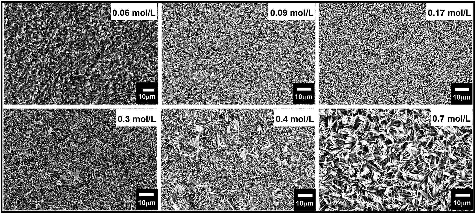 | ||
| Fig. 5 FE-SEM micrographs of vertically aligned α-MoO3 nano-blades prepared by varying the acid molar concentration at a growth temperature of 180 °C on the seeded substrate of 10/100 nm of Cr/MoO3. | ||
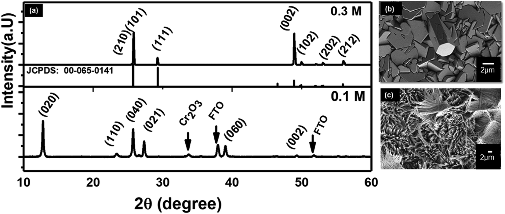 | ||
| Fig. 6 XRD patterns of MoO3 nanostructures at a different molar concentration at 180 °C using seed layer of Cr/MoO3 of 10/100 nm (a) 0.1 M and 0.3 M. FE-SEM images of MoO3 nanostructures at a different molar concentration (b) 0.1 M and (c) 0.3 M. | ||
The reaction temperature was found to have a minor effect on the morphology between 100 and 200 °C as shown in Fig. 7, in line with previous reports using in situ EXAFS, in which the formation of α-MoO3 rods above a threshold of 100 °C was observed.54
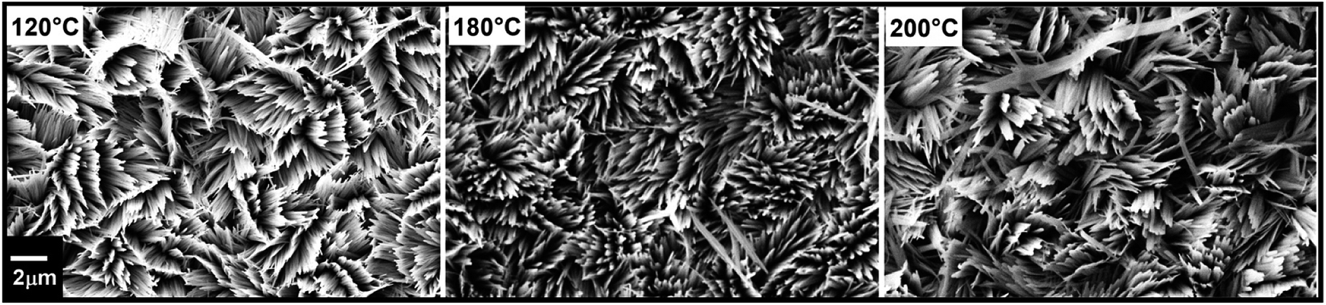 | ||
| Fig. 7 FE-SEM micrographs of vertically aligned α-MoO3 nano-blades prepared at different hydrothermal reaction's temperatures using acid molar concentration of 0.3 mol L−1 and seed layer of 10/100 nm of Cr/MoO3. | ||
The uniform length of the nanowires and flower-like shapes in which they are arranged on the substrate leads to the conclusion that growth occurs exclusively from the seed particles, and the orientation perpendicular to the substrate is caused by the blades mutually pushing each other up when they start touching (Fig. 4).
While the conditions of the hydrothermal reaction can be tuned to reach optimal conditions for fast growth of a MoO3 film with a high surface area, the adhesion layer is crucial to accommodate a wide range of different substrates with significant variations in roughness. Rougher substrates required less Cr deposited for the MoO3 film to adhere to the substrate, with FTO requiring a 5–10 nm layer and Si/SiO2 requiring 10–20 nm.
4 Conclusion
In summary, we have presented a simple, fast, and highly reproducible strategy to grow vertically aligned, crystalline α-MoO3 nano-blades on Si/SiO2 and FTO substrates under hydrothermal conditions. The synthesis procedure consists of two steps, seed layer formation and seeded growth of highly anisotropic nano-blades by hydrothermal method. The reaction time could be reduced 50-fold compared to literature methods for dispersed α-MoO3 nanostructures. The synthesis procedure allows a simple, fast, and large-scale fabrication of vertically aligned nanostructures on different substrates. Reaction time and precursor concentration were found to be the principal parameters to control the shape and aspect ratio of the nano-blades, with a phase transition from orthorhombic α-MoO3 to hexagonal h-MoO3 occurring at high precursor and acid concentrations. The developed procedure of the vertically aligned nanostructure α-MoO3 with high surface area might be favourable for several devices such as gas sensors, supercapacitors, batteries, and others.Conflicts of interest
There are no conflicts to declare.Acknowledgements
The authors sincerely acknowledge Dr Balasubramanaim Saravanakumar “School for Advanced Research in Polymers (SARP), Laboratory for Advanced Research in Polymeric Materials (LARPM), Central Institute of Plastic Engineering and Technology (CIPET), Bhubaneswar, INDIA” for valuable discussion and revision. The authors appreciate the support of Dr Marina Krumova, Z. K. Chen and Dr Peyman Zirak “Chemistry Department, University of Konstanz, Germany” for acquiring TEM data and Raman spectra and discussion and the lab-technician Said Riazi. The work was supported by the Deutsche Forschungsgemeinschaft (DFG) through the Collaborative Research Center SFB 1214 project Z1 (Particle Analysis Center). K. B. acknowledges support by the Zukunftskolleg Konstanz through a 5-Year Research Fellowship.References
- R. K. Sharma and G. B. Reddy, J. Phys. D: Appl. Phys., 2014, 47, 065305 CrossRef.
- P. C. Kao, S. C. Lin, C. C. Hsueh, W. T. Liu, H. E. Yen and Z. L. Tseng, J. Nanoelectron. Optoelectron., 2017, 12, 857–861 CrossRef CAS.
- W. Wang, J. Qin, Z. Yin and M. Cao, ACS Nano, 2016, 10, 10106–10116 CrossRef CAS PubMed.
- F. Ji, X. Ren, X. Zheng, Y. Liu, L. Pang, J. Jiang and S. F. Liu, Nanoscale, 2016, 8, 8696–8703 RSC.
- Y. R. Shen, P. P. Jiang, P. T. Wai, Q. Gu and W. J. Zhang, Catalysts, 2019, 9, 31 CrossRef.
- J. B. Zhou, N. Lin, L. B. Wang, K. L. Zhang, Y. C. Zhu and Y. T. Qian, J. Mater. Chem. A, 2015, 3, 7463–7468 RSC.
- B. Y. Zhang, A. Zavabeti, A. F. Chrimes, F. Haque, L. A. O'Dell, H. Khan, N. Syed, R. Datta, Y. Wang, A. S. R. Chesman, T. Daeneke, K. Kalantar-zadeh and J. Z. Ou, Adv. Funct. Mater., 2018, 28, 1706006 CrossRef.
- R. S. Datta, F. Haque, M. Mohiuddin, B. J. Carey, N. Syed, A. Zavabeti, B. Zhang, H. Khan, K. J. Berean, J. Z. Ou, N. Mahmood, T. Daeneke and K. Kalantar-zadeh, J. Mater. Chem. A, 2017, 5, 24223–24231 RSC.
- A. P. Daniela Nunes, L. Santos, B. Pedro, L. Pereira, E. Fortunato and R. Martins, Metal Oxide Nanostructures: Synthesis, Properties and Applications, Elsevier, Amsterdam, 2018 Search PubMed.
- K. Inzani, T. Grande, F. Vullum-Bruer and S. M. Selbach, J. Phys. Chem. C, 2016, 120, 8959–8968 CrossRef CAS.
- L. Jiwen, Int. J. Electrochem. Sci., 2017, 2429–2440 CrossRef.
- N. Illyaskutty, S. Sreedhar, G. Sanal Kumar, H. Kohler, M. Schwotzer, C. Natzeck and V. P. M. Pillai, Nanoscale, 2014, 6, 13882–13894 RSC.
- D. D. Yao, J. Z. Ou, K. Latham, S. Zhuiykov, A. P. O'Mullane and K. Kalantar-zadeh, Cryst. Growth Des., 2012, 12, 1865–1870 CrossRef CAS.
- R. Kumar, AIP Conf. Proc., 2017, 1860, 020011 CrossRef.
- S. Ashraf, C. S. Blackman, G. Hyett and I. P. Parkin, J. Mater. Chem., 2006, 16, 3575–3582 RSC.
- P. Balasubramanian, M. Annalakshmi, S.-M. Chen and T.-W. Chen, Ultrason. Sonochem., 2019, 50, 96–104 CrossRef CAS PubMed.
- L. Cai, C. J. McClellan, A. L. Koh, H. Li, E. Yalon, E. Pop and X. Zheng, Nano Lett., 2017, 17, 3854–3861 CrossRef CAS PubMed.
- K. Sakaushi, J. Thomas, S. Kaskel and J. Eckert, Chem. Mater., 2013, 25, 2557–2563 CrossRef CAS.
- W. J. Dong, J. Ham, G. H. Jung, J. H. Son and J. L. Lee, J. Mater. Chem. A, 2016, 4, 4755–4762 RSC.
- S. A. Khalate, R. S. Kate, H. M. Pathan and R. J. Deokate, J. Solid State Electrochem., 2017, 21, 2737–2746 CrossRef CAS.
- J. M. Romo-Herrera, M. Terrones, H. Terrones, S. Dag and V. Meunier, Nano Lett., 2007, 7, 570–576 CrossRef CAS PubMed.
- Z. U. Abideen, J.-H. Kim, J.-H. Lee, J.-Y. Kim, A. Mirzaei, H. W. Kim and S. S. Kim, J. Korean Ceram. Soc., 2017, 54, 366–379 CrossRef.
- S. J. Pearton and F. Ren, Nanomater. Nanotechnol., 2013, 3, 1 CrossRef.
- R. Ahmad, S. M. Majhi, X. Zhang, T. M. Swager and K. N. Salama, Adv. Colloid Interface Sci., 2019, 270, 1–27 CrossRef CAS PubMed.
- S. Choopun, N. Hongsith and E. Wongrat, in Nanowires - Recent Advances, 2012, ch. 1, DOI:10.5772/54385.
- Gas Sensors Based on Conducting Metal Oxides, ed. N. Barsan and K. Schierbaum, Elsevier, 2019, pp. xxi–xxiii, DOI:10.1016/B978-0-12-811224-3.00010-X.
- A. Ponzoni, C. Baratto, N. Cattabiani, M. Falasconi, V. Galstyan, E. Nunez-Carmona, F. Rigoni, V. Sberveglieri, G. Zambotti and D. Zappa, Sensors, 2017, 17, 714 CrossRef PubMed.
- I. Gonzalez-Valls and M. Lira-Cantu, Energy Environ. Sci., 2009, 2, 19–34 RSC.
- J. Zhou, S. Z. Deng, N. S. Xu, J. Chen and J. C. She, Appl. Phys. Lett., 2003, 83, 2653–2655 CrossRef CAS.
- R. K. Sharma and G. B. Reddy, J. Appl. Phys., 2013, 114, 184310 CrossRef.
- B. Yan, Z. Zheng, J. Zhang, H. Gong, Z. Shen, W. Huang and T. Yu, J. Phys. Chem. C, 2009, 113, 20259–20263 CrossRef CAS.
- J. Liu, L. He, L. Wang, Y. Man, L. Huang, Z. Xu, D. Ge, J. Li, C. Liu and L. Wang, ACS Appl. Mater. Interfaces, 2016, 8, 30576–30582 CrossRef CAS PubMed.
- M. Todeschini, A. Bastos da Silva Fanta, F. Jensen, J. B. Wagner and A. Han, ACS Appl. Mater. Interfaces, 2017, 9, 37374–37385 CrossRef CAS PubMed.
- N. Schönberg, W. G. Overend, A. Munthe-Kaas and N. A. Sörensen, Acta Chem. Scand., 1954, 8, 221–225 CrossRef.
- C. Palacio, H. J. Mathieu and D. Landolt, Surf. Sci., 1987, 182, 41–55 CrossRef CAS.
- P. H. H. G. Thurner, Acta Phys. Pol., A, 1992, 81, 273–283 CrossRef.
- L. H. Gaabour, J. Mater. Res. Technol., 2019, 8, 2157–2163 CrossRef CAS.
- C. W. P. Benjamin, Proc. R. Soc. London, Ser. A, 1961, 261, 516–531 Search PubMed.
- R. C. Williams and R. C. Backus, J. Appl. Phys., 1949, 20, 98–106 CrossRef CAS.
- P. Benjamin and C. Weaver, Proc. R. Soc. London, Ser. A, 1960, 254, 163–176 CAS.
- P. H. Holloway, Gold Bull., 1979, 12, 99–106 CrossRef CAS.
- S. C. Jain, A. H. Harker and R. A. Cowley, Philos. Mag. A, 1997, 75, 1461–1515 CAS.
- A. Chithambararaj, N. S. Sanjini, S. Velmathi and A. C. Bose, Phys. Chem. Chem. Phys., 2013, 15, 14761–14769 RSC.
- K. Dewangan, N. N. Sinha, P. K. Sharma, A. C. Pandey, N. Munichandraiah and N. S. Gajbhiye, CrystEngComm, 2011, 13, 927–933 RSC.
- S. Guimond, D. Göbke, J. M. Sturm, Y. Romanyshyn, H. Kuhlenbeck, M. Cavalleri and H. J. Freund, J. Phys. Chem. C, 2013, 117, 8746–8757 CrossRef CAS.
- Y. Song, J. Zhao, Y. Zhao, Z. Huang, Y. Li and G. Wu, CrystEngComm, 2016, 18, 6502–6512 RSC.
- A. Michailovski, J.-D. Grunwaldt, A. Baiker, R. Kiebach, W. Bensch and G. R. Patzke, Angew. Chem., Int. Ed., 2005, 44, 5643–5647 CrossRef CAS PubMed.
- M. Niederberger, F. Krumeich, H.-J. Muhr, M. Muller and R. Nesper, J. Mater. Chem., 2001, 11, 1941–1945 RSC.
- Z. Peng, Nanofibers - Production, Properties and Functional Applications "Preparation and Characterization and Reducing Properties of MoO3 Nano-Fibers", IntechOpen, 2011 Search PubMed.
- H.-Y. Li, L. Huang, X.-X. Wang, C.-S. Lee, J.-W. Yoon, J. Zhou, X. Guo and J.-H. Lee, RSC Adv., 2017, 7, 3680–3685 RSC.
- G. R. Patzke, A. Michailovski, F. Krumeich, R. Nesper, J. D. Grunwaldt and A. Baiker, Chem. Mater., 2004, 16, 1126–1134 CrossRef CAS.
- G. R. Patzke, F. Krumeich and R. Nesper, Angew. Chem., Int. Ed., 2002, 41, 2446–2461 CrossRef CAS.
- D. F. Alexandru Grumezescu, Nanostructures for Novel Therapy, Elsevier, 2017 Search PubMed.
- A. Michailovski and G. R. Patzke, Chemistry, 2006, 12, 9122–9134 CrossRef CAS PubMed.
Footnote |
| † Electronic supplementary information (ESI) available. See DOI: 10.1039/d0ra01281e |
| This journal is © The Royal Society of Chemistry 2020 |