DOI:
10.1039/D0RA04145A
(Paper)
RSC Adv., 2020,
10, 24127-24133
Electronic structure, optoelectronic properties and enhanced photocatalytic response of GaN–GeC van der Waals heterostructures: a first principles study
Received
8th May 2020
, Accepted 12th June 2020
First published on 24th June 2020
Abstract
In this work, we systematically studied the electronic structure and optical characteristics of van der Waals (vdW) heterostructure composed of a single layer of GaN and GeC using first principles calculations. The GaN–GeC vdW heterostructure exhibits indirect band gap semiconductor properties and possesses type-II energy band arrangement, which will help the separation of photogenerated carriers and extend their lifetime. In addition, the band edge positions of the GaN–GeC heterostructure meet both the requirements of water oxidation and reduction energy, indicating that the photocatalysts have the potential for water decomposition. The GaN–GeC heterostructure shows obvious absorption peaks in the visible region, leading to the efficient use of solar energy. Tensile and compressive strains of up to 10% are also proposed. Tensile strain leads to an increase in the blue shift of optical absorption, whereas a red shift is observed in the case of the compressive strain. These fascinating characteristics make the GaN–GeC vdW heterostructure a highly effective photocatalyst for water splitting.
1 Introduction
Following the successful exfoliation of graphene, scientists are motivated to the research of new two-dimensional materials (2D) owing to their distinctive physical properties and promising application in optoelectronics and photocatalytics.1–9 Among these 2D materials, graphene like hexagonal GeC and GaN monolayers have gained much attention due to their wide band gap, which makes them suitable for designing optoelectronics, photovoltaic devices, and heterostructures.10–12 Experimentally, GeC monolayer was first prepared by the chemical vapor deposition (CVD) technique13 and laser ablation.14,15 2D GeC monolayer has a planar structure which is dynamically stable and has a good optoelectronic performance.16–18 Due to the higher Poisson's ratio and lower stiffness of GeC monolayer as compared to graphene,19 it achieves enhanced electronic, optoelectronic, and photovoltaic device applications.20 Similar to GeC monolayer, graphene-like gallium nitride (g-GaN) has also received much attention due to its semiconducting character with a wide band of about 4 eV.21 The GaN monolayer has also been successfully fabricated in experiment from the migration-enhanced encapsulated-growth.22 Based on the progress of 2D material synthesis, a new exciting field is emerged to assemble separated 2D materials into numerical layered heterostructures in a precisely controlled sequence, namely vdW heterostructures.23–27 These structures will provide many novel platforms for conducting new phenomena and fabricating future nanoelectronic devices. Due to the weak interlayer interactions, occurring in these layered vdW heterostructures, they can be easily fabricated in various common techniques. So far, many vertical stacked vdW heterostructures have been theoretically predicted, even though experiments, and used to manufacture nanodevices with desired characteristics and unique functions.28–33 Most recently, GeC–MSSe (M = Mo, W), g-GaN-transition metal dichalcogenides,34 blueP–SiC–BSe heterostructures,35 Janus–Janus heterostructures,36 TMDCs–TMDCs heterostructures,37 SiC–TMDCs heterostructures38 and SnSe2–MoS2 (ref. 39) heterostructures have been predicted theoretically and fabricated experimentally. More interestingly, these heterostructures exhibit acceptable band alignments for the redox potentials of water, making them promising candidate for water splitting applications. Furthermore, GeC and GaN monolayers have the same hexagonal structure, resulting in a small difference in lattice parameters, providing a beneficial to the growth of GeC–GaN bilayer in experiment. In view of all above mentioned studies, in this work, the electronic structure, charge transfer, optical and photocatalytic properties of GeC–GaN vdW heterostructures are investigated using first-principles calculations. Our results shows that GeC–GaN heterostructures could be a promising material for future optoelectronics and photocatalytics.
2 Computational methods
In this work, all the electronic and optoelectronic properties of GeC–GaN heterostructure are investigated through first-principles calculation,40 which is implemented in Vienna ab initio simulations.41,42 To describe the weak vdW interactions, we used Perdew–Burke–Ernzerhof generalized gradient approximation (PBE-GGA).43 The cutoff energy for plane wave basis is set to be 500 eV. We set the forces of 0.01 eV Å−1 for atomic positions relaxation, while energy conversion criterion is set to be 10−5 eV. A vacuum space of 25 Å is added along the z direction of heterostructure to prevent possible periodic boundary conditions. It is clear that the PBE-GGA underestimates the band gaps of materials, so here we used hybrid Heyd–Scuseria–Ernzerhof (HSE06)44 to obtain a more accurate band gap value. To check the thermal stability of these systems, we used the ab initio molecular dynamics simulations (AIMD).45 Phonon dispersions were obtained by the interatomic-force-constant matrix with a grid of (9 × 9 × 1) k-point mesh using density functional perturbation theory (DFPT).
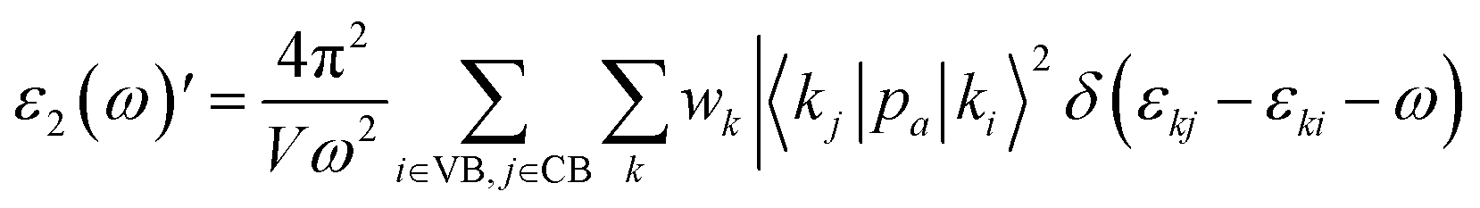
The imaginary part of dielectric function is calculated as follows:
| |
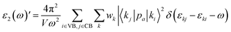 | (1) |
Here,
V and
ω represent the unit cell volume and photon frequency, respectively. With considering an effective unit cell volume (
Veff), the imaginary part of dielectric function can be rewritten as:
46| |
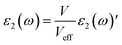 | (2) |
3 Results and discussion
We first check the lattice parameters and electronic properties of the constituent GaN and GeC monolayers. The optimized structure of GaN and GeC monolayers is depicted in Fig. 1. The lattice constant of GaN and GeC monolayers is calculated to be 3.26 Å and 3.25 Å, respectively. The lattice mismatch in the GeC–GaN heterostructure is very small of about 0.3%, making it easy to form a stable 2D heterostructure. The band structures of GaN and GeC monolayers are calculated by HSE06 method as shown in Fig. 2. The band gap of GaN and GeC monolayers is 3.19 eV and 3.20 eV, respectively. The GaN monolayer has an indirect band gap semiconductor with the valence band maximum (VBM) at K-point and the conduction band maximum (CBM) at Γ point. While, the GeC monolayer is a direct band gap semiconductor both the CBM and VBM at the K-point. All these results are comparable with previous reports.17,18,47
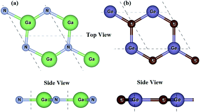 |
| | Fig. 1 Top view and side view of (a) GaN and (b) GeC monolayers. | |
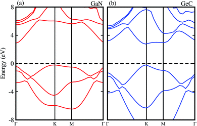 |
| | Fig. 2 Electronic band structure obtained by HSE06 method of (a) GaN (b) GeC monolayers, respectively. | |
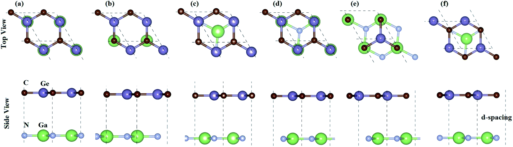
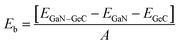
For GeC–GaN heterostructure, we consider six possible staking configurations, as depicted in Fig. 3. For stacking-1, a Ge atom is on top of a Ga atom while a C atom is on top of a N atom; for stacking-2, a C atom is placed on top of a Ga atom and a Ge atom is on top of a N atom; for stacking-3, a Ge is on a top of a N atom, while a C atom is centered at a Ge–C hexagonal ring; for stacking-4, a Ge atom is on top of a Ga atom, while a C atom is centered at a Ge–C hexagonal ring; for stacking-5, a C atom is on top of a Ga atom, while a Ge is centered at a Ge–C hexagonal ring; for stacking-6, a C atom is placed on top of a N atom, while a Ga atom is centered at a Ge–C hexagonal ring. All these configurations are illustrated in Fig. 3. To compare all these stacking configurations, we further calculate their binding energies and interlayer spacing48,49 as follows:
| |
 | (3) |
Here,
EGeC–GaN,
EGeC and
EGaN represent the total energies of GeC–GaN heterostructure, isolated GeC and GaN monolayers, respectively.
A represents the surface area of such heterostructure. The calculated binding energy of GeC–GaN heterostructure for different stacking configurations is listed in
Table 1.
 |
| | Fig. 3 Possible stacking configurations of GeC–GaN vdW heterostructure; (a) stacking-1, (b) stacking-2, (c) stacking-3, (d) stacking-4, (e) stacking-5, (f) stacking-6, respectively. | |
Table 1 Calculated interlayer distance (Å), binding energy (meV Å−2), band gap (eV), band nature and band alignment of the GaN–GeC heterostructure for different stacking configurations
| |
D |
Eb |
Eg (PBE/HSE) |
Band nature |
Band alignment |
| Stacking-1 |
3.24 |
−39.81 |
1.52/2.21 |
Indirect |
Type-II |
| Stacking-2 |
3.21 |
−40.61 |
1.97/2.76 |
Indirect |
Type-II |
| Stacking-3 |
3.32 |
−36.66 |
1.28/2.16 |
Indirect |
Type-II |
| Stacking-4 |
3.35 |
−34.97 |
1.30/2.23 |
Indirect |
Type-II |
| Stacking-5 |
3.34 |
−35.14 |
1.96/2.89 |
Indirect |
Type-II |
| Stacking-6 |
3.31 |
−37.46 |
1.92/2.85 |
Indirect |
Type-II |
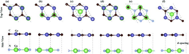
One can find from Table 1 that the interlayer distance of the GaN–GeC heterostructure for different stacking configurations are ranging from 3.21 Å to 3.35 Å. It is clear that these values of interlayer distance are comparable with those in other vdW-typical heterostructures.50 The stacking-2 of the GaN–GeC heterostructure has the smallest interlayer distance as compared to others one. Furthermore, we can find that the negative value of the binding energy indicates that the GaN–GeC heterostructure for six stacking configurations is energetically stable. The stacking-2 of the GaN–GeC heterostructure has the lowest binding energy. The shortest interlayer distance of 3.21 Å and the lowest binding energy of −40.61 meV Å−2 as listed in Table 1 demonstrate that the stacking-2 is the most energetically favorable stacking configuration of the GaN–GeC heterostructure. In addition, it is clear that the binding energy values of the GaN–GeC heterostructure for six stacking configurations are comparable with those of other vdW heterostructures.21,51,52 These findings demonstrate that the GaN–GeC heterostructure for six stacking configurations is characterized by the weak vdW forces. We further perform the AIMD simulation of the most stable structure to check its thermal stability at room temperature of 300 K for total 6 ps with a time interval of 1 fs, as displayed in Fig. 4. One can find from Fig. 4 that there is no distortion in the atomic structure of the GeC–GaN heterostructure after heating 6 ps. Moreover, we find that the fluctuation of the total energy of the GaN–GeC heterostructure befor and after heating 6 ps is very small. All these findings indicate that the GaN–GeC heterostructure retains its geometries without any structural distortion, confirming the thermal stability of such heterostructure.
 |
| | Fig. 4 Snapshots of the atomic structure of the most energetically favorable stacking configuration of GeC–GaN heterostructure (a) before and (b) after heating 6 ps. (c) AIMD simulation of the fluctuations of total energy as a function of the time step at room temperature. | |
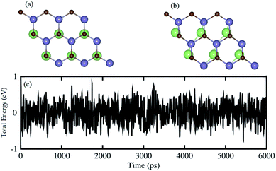
The projected and weighted band structures of the most energetically favorable stacking configuration of GeC–GaN vdW heterostructure are illustrated in Fig. 5. It is clear that the GeC–GaN vdW heterostructure is an indirect band gap semiconductor with the VBM at Γ point and the CBM at the K-point. The calculated band gap value given from PBE and HSE06 methods of the GeC–GaN vdW heterostructure is 1.97 eV and 2.76 eV, respectively. Such band gap value of the GeC–GaN vdW heterostructure is smaller than that of both individual GeC and GaN monolayers,17,18,47 showing that the formation of vdW heterostructure results in a reduction of the band gap. Interestingly, the band gap of the GeC–GaN vdW heterostructure for both PBE and HSE calculation is greater than the required band gap of photocatalyst (1.23 eV), confirming potential application of GeC–GaN vdW heterostructure as a visible light photocatalyst.53 To check GeC–GaN vdW heterostructure for type-I and type-II band alignment, we provide the weighted band structures of such vdW heterostructures, as illustrated in Fig. 5(c). One can find that the VBM of the GeC–GaN heterostructure comes from the GaN monolayer, while its CBM is contributed by the GeC monolayer, resulting in the formation of the type-II band alignment, which will spontaneously separate the free electrons and holes, enabling the high efficiency optoelectronics and solar energy conversions.32,50 Moreover, it is clear from Fig. 5(c) that the VBM is due to the N-pz orbitals of the GaN monolayer, while the CBM comes from the Ge-pz orbitals of the GeC monolayer. This orbital overlaps can modify the orbitals and can enhance the optical absorption.
 |
| | Fig. 5 Electronic band structure of the GeC–GaN vdW heterostructure obtained from (a) PBE and (b) HSE06 method. (c) The weighted band structure of GeC–GaN vdW heterostructure. | |
To further understand the charge redistribution of the GaN–GeC heterostructure, we calculate the charge density difference, which can be obtained as follows:
| | |
Δρ = ρGaN–GeC − ρGaN − ρGeC
| (4) |
Here,
ρGaN–GeC,
ρGaN and
ρGeC, respectively, are the charge densities of GaN–GeC heterostructure, the constituent GaN and GeC monolayers. The charge density difference of the GaN–GeC heterostructure is displayed in the inset of
Fig. 6(a). The yellow and cyan regions represent the charge accumulation and depletion, respectively. It demonstrates that the charges are mainly accumulated in the side of GeC layer, whereas the charge depletion is observed around the GaN layer. It indicates that the electrons are transferred from the GaN to the GeC layer in the GaN–GeC heterostructure. To present a qualitative understanding of the charge transfer in the GeC–GaN vdW heterostructure, we further perform the Bader charge analysis, as shown in
Fig. 6(a). Bader charge analysis shows that about 0.12 electrons are transferred from the GaN to the GeC layer. The small amount of charge transfer can be linked with the close atomic electronegativity values (Ga-1.81, N-3.04, Ge-2.01, C-2.55). In addition, the electrostatic potential of the GeC–GaN heterostructure indicates that the GeC layer has a deeper potential than the GaN layer, driving electrons to move from the GaN layer to GeC. The potential drop (Δ
V) across the bilayer is found to be 5.2 eV. Consequently, the excitonic behavior of GeC–GaN vdW heterostructure is quite different from that of the isolated layers, facilitating the separation of electrons and holes.
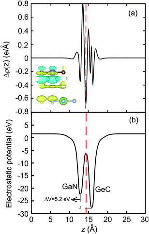 |
| | Fig. 6 (a) The plane averaged charge density difference and (b) electrostatic potential of GaN–GeC vdW heterostructure along the z direction. ΔV represents the potential drop. The inset in (a) represents the charge density difference in GaN–GeC heterostructure. | |
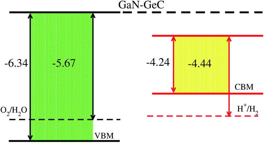
The calculated imaginary part of dielectric function in Fig. 7 demonstrates that the GeC–GaN vdW heterostructure possesses a first absorption peak at the visible region of 619.9 nm, and several peaks that almost cover nearly the entire incident solar spectrum.54 Therefore, it is obvious that the GeC–GaN vdW heterostructure acts as a high-performance absorber of sunlight, which is useful for attaining high-efficiency photocatalyst. Furthermore, to gain more insight into the possible application of the GeC–GaN vdW heterostructure in photocatalyst, we use Mulliken electronegativity method54,55 to check GeC–GaN vdW heterostructure as water splitting at acidic solution, as illustrated in Fig. 8. It is obvious that the VBM and CBM of the GeC–GaN heterostructure are higher than those of standard redox potentials, providing enough force to drive the photogenerated electrons and holes to dissociate water into H+ = H2 and O2 = H2O for acidic solution. It should be noted that both monolayers GeC and GaN have favorable band positions for water splitting at pH = 0, but their oversize band gaps are unfavorable to absorb solar spectrum, reducing their potential conversion efficiency.56 Therefore, it is verifying that the GeC–GaN vdW heterostructure might have promising applications for hydrogen generation in both acidic and neutral environments by water splitting.
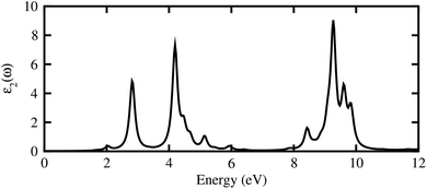 |
| | Fig. 7 Imaginary part of dielectric functions of GeC–GaN vdW heterostructure as a function of photon energy. | |
 |
| | Fig. 8 Band alignment of GeC–GaN vdW heterostructure with respect to the redox potentials of water. | |
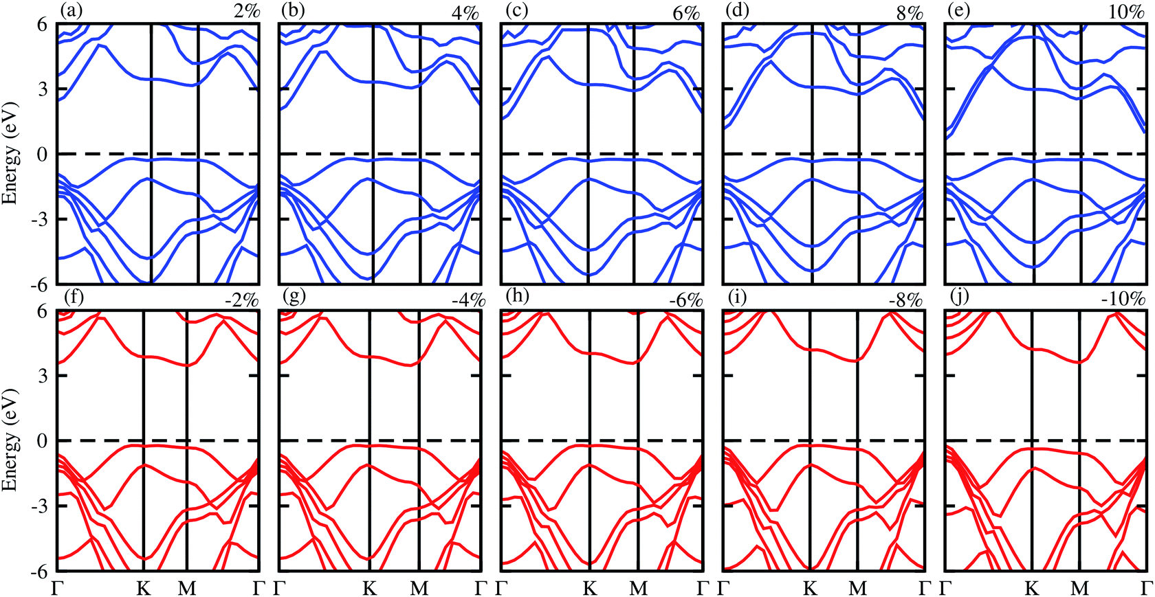
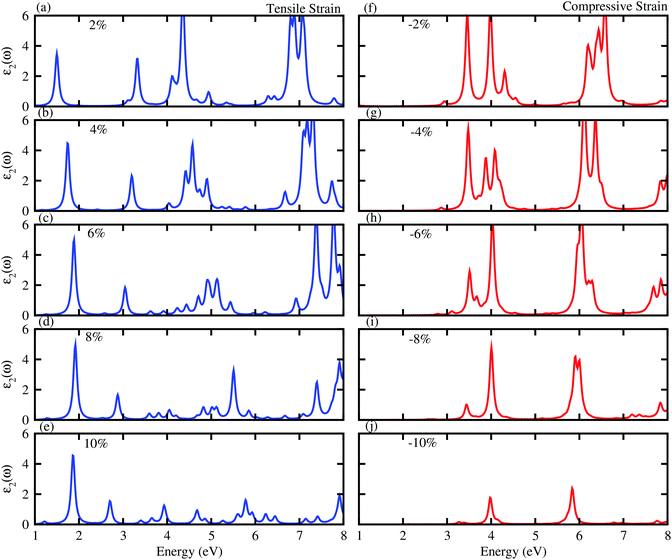
Next, we will discuss the effect of strain on the band alignment and optical properties of the GeC–GaN heterostructure. The phonon dispersion curves of the GeC–GaN heterostructure without and with the presence of large tensile and compressive strains are depicted in Fig. 9. One can find from Fig. 9 that the GaN–GeC heterostructure are mechanical stability under large compressive and tensile strains of 10% with no negative frequencies. The band structures of the GeC–GaN heterostructure under different tensile and compressive strains are depicted in Fig. 10. One can see that by applying the tensile strain the band gap of GeC–GaN vdW heterostructure slowly decreases, while such band gap increases with increasing the compressive strain. We also consider the changes in the imaginary part of dielectric function of the GeC–GaN heterostructure under different tensile and compressive strains, as depicted in Fig. 11. With the presence of the tensile strain, there is an increase in the blue shift of optical absorption, whereas the red shift is observed in the case of the compressive strain. These fascinating characteristics make the GaN–GeC vdW heterostructure a highly effective photocatalyst for water splitting.
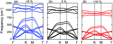 |
| | Fig. 9 Phonon spectra of the GaN–GeC heterostructure under different strains of (a) −10% (compressive strain), (b) 0% (unstrained state) and (c) +10% (tensile strain), respectively. | |
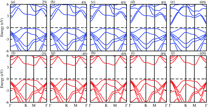 |
| | Fig. 10 Electronic band structure of tensile (blue) and compressive strain (red) of GeC–GaN vdW heterostructure. | |
 |
| | Fig. 11 Imaginary part of dielectric function of tensile (blue) and compressive strain (red) of GeC–GaN vdW heterostructure. | |
4 Conclusions
In summary, through the first principle calculations, we have investigated the electronic, optical and photocatalytic properties of the GeC–GaN vdW heterostructure as well as the effects of tensile and compressive strains. The GeC–GaN vdW heterostructure is an indirect band gap semiconductor with type-II band alignment. In the GeC–GaN vdW heterostructure the GaN layer donates electrons to GeC layers. The GeC–GaN vdW heterostructure also exhibits a significant optical absorption in visible region. The band edges of GeC–GaN vdW heterostructure straddle the redox potential, hence showing potential photocatalysts for water splitting. Furthermore, our findings reveal that strains can tune both the band alignment and optical absorptions of the GeC–GaN heterostructure, making it promising candidate for enhanced photocatalytic activity of hydrogen generation from water. Our results also can provide valuable guidance for synthesis of GeC–GaN vdW heterostructure and for its potential applications as photocatalysts.
Conflicts of interest
There are no conflicts to declare.
References
- J. Nakamura, T. Nitta and A. Natori, Phys. Rev. B: Condens. Matter Mater. Phys., 2005, 72, 205429 CrossRef.
- A. Du, S. C. Smith and G. Lu, Chem. Phys. Lett., 2007, 447, 181–186 CrossRef CAS.
- Y. Li, Z. Zhou, S. Zhang and Z. Chen, J. Am. Chem. Soc., 2008, 130, 16739–16744 CrossRef CAS PubMed.
- L. Li, Y. Yu, G. J. Ye, Q. Ge, X. Ou, H. Wu, D. Feng, X. H. Chen and Y. Zhang, Nat. Nanotechnol., 2014, 9, 372 CrossRef CAS PubMed.
- H. O. Churchill and P. Jarillo-Herrero, Nat. Nanotechnol., 2014, 9, 330–331 CrossRef CAS PubMed.
- H. Liu, A. T. Neal, Z. Zhu, Z. Luo, X. Xu, D. Tománek and P. D. Ye, ACS Nano, 2014, 8, 4033–4041 CrossRef CAS PubMed.
- D. J. Late, B. Liu, J. Luo, A. Yan, H. R. Matte, M. Grayson, C. Rao and V. P. Dravid, Adv. Mater., 2012, 24, 3549–3554 CrossRef CAS PubMed.
- Q. Tang and Z. Zhou, Prog. Mater. Sci., 2013, 58, 1244–1315 CrossRef CAS.
- Q. Tang, Z. Zhou and Z. Chen, Wiley Interdiscip. Rev.: Comput. Mol. Sci., 2015, 5, 360–379 CAS.
- A. Hao, X. Yang, X. Wang, Y. Zhu, X. Liu and R. Liu, J. Appl. Phys., 2010, 108, 063531 CrossRef.
- S. Lin, Y. Lu, J. Xu, S. Feng and J. Li, Nano Energy, 2017, 40, 122–148 CrossRef CAS.
- J. Szmidt, M. Gazicki-Lipman, H. Szymanowski, R. Mazurczyk, A. Werbowy and A. Kudła, Thin Solid Films, 2003, 441, 192–199 CrossRef CAS.
- X. Wu, W. Zhang, L. Yan and R. Luo, Thin Solid Films, 2008, 516, 3189–3195 CrossRef CAS.
- H. Yuan and R. S. Williams, Chem. Mater., 1993, 5, 479–485 CrossRef CAS.
- H. Shafi, A. Mahmood, Z. Ali and M. Mehmood, Key Eng. Mater., 2010, 178–186 CAS.
- L. Drissi and F. Ramadan, Phys. E, 2015, 74, 377–381 CrossRef CAS.
- H. Şahin, S. Cahangirov, M. Topsakal, E. Bekaroglu, E. Akturk, R. T. Senger and S. Ciraci, Phys. Rev. B: Condens. Matter Mater. Phys., 2009, 80, 155453 CrossRef.
- L. Pan, H. Liu, Y. Wen, X. Tan, H. Lv, J. Shi and X. Tang, Phys. Lett. A, 2011, 375, 614–619 CrossRef CAS.
- Q. Peng, C. Liang, W. Ji and S. De, Mech. Mater., 2013, 64, 135–141 CrossRef.
- K. Ren, M. Sun, Y. Luo, S. Wang, Y. Xu, J. Yu and W. Tang, Phys. Lett. A, 2019, 383, 1487–1492 CrossRef CAS.
- M. Sun, J.-P. Chou, Q. Ren, Y. Zhao, J. Yu and W. Tang, Appl. Phys. Lett., 2017, 110, 173105 CrossRef.
- Z. Y. Al Balushi, K. Wang, R. K. Ghosh, R. A. Vilá, S. M. Eichfeld, J. D. Caldwell, X. Qin, Y.-C. Lin, P. A. DeSario and G. Stone, et al., Nat. Mater., 2016, 15, 1166–1171 CrossRef CAS PubMed.
- K. Novoselov, A. Mishchenko, A. Carvalho and A. C. Neto, Science, 2016, 353, aac9439 CrossRef CAS PubMed.
- W. Yu, Z. Zhu, S. Zhang, X. Cai, X. Wang, C.-Y. Niu and W.-B. Zhang, Appl. Phys. Lett., 2016, 109, 103104 CrossRef.
- Y. Huang, X. Chen, C. Wang, L. Peng, Q. Qian and S. Wang, Nanoscale, 2017, 9, 8616–8622 RSC.
- L. Peng, C. Wang, Q. Qian, C. Bi, S. Wang and Y. Huang, ACS Appl. Mater. Interfaces, 2017, 9, 40969–40977 CrossRef CAS PubMed.
- C. Wang, L. Peng, Q. Qian, J. Du, S. Wang and Y. Huang, Small, 2018, 14, 1703536 CrossRef PubMed.
- Z.-S. Wu, Y. Zheng, S. Zheng, S. Wang, C. Sun, K. Parvez, T. Ikeda, X. Bao, K. Müllen and X. Feng, Adv. Mater., 2017, 29, 1602960 CrossRef PubMed.
- M. Long, E. Liu, P. Wang, A. Gao, H. Xia, W. Luo, B. Wang, J. Zeng, Y. Fu and K. Xu, et al., Nano Lett., 2016, 16, 2254–2259 CrossRef CAS PubMed.
- D. Li, X. Wang, Q. Zhang, L. Zou, X. Xu and Z. Zhang, Adv. Funct. Mater., 2015, 25, 7360–7365 CrossRef CAS.
- X.-H. Li, B.-J. Wang, X.-L. Cai, L.-W. Zhang, G.-D. Wang and S.-H. Ke, RSC Adv., 2017, 7, 28393–28398 RSC.
- X.-H. Li, B.-J. Wang, X.-L. Cai, W.-Y. Yu, L.-W. Zhang, G.-D. Wang and S.-H. Ke, RSC Adv., 2017, 7, 44394–44400 RSC.
- Q. Zhang, X. Xiao, R. Zhao, D. Lv, G. Xu, Z. Lu, L. Sun, S. Lin, X. Gao and J. Zhou, et al., Angew. Chem., Int. Ed., 2015, 54, 8957–8960 CrossRef CAS PubMed.
- H. Din, M. Idrees, A. Albar, M. Shafiq, I. Ahmad, C. V. Nguyen and B. Amin, Phys. Rev. B, 2019, 100, 165425 CrossRef CAS.
- M. Idrees, H. Din, S. Khan, I. Ahmad, L.-Y. Gan, C. V. Nguyen and B. Amin, J. Appl. Phys., 2019, 125, 094301 CrossRef.
- M. Idrees, H. Din, R. Ali, G. Rehman, T. Hussain, C. Nguyen, I. Ahmad and B. Amin, Phys. Chem. Chem. Phys., 2019, 21, 18612–18621 RSC.
- B. Amin, N. Singh and U. Schwingenschlögl, Phys. Rev. B: Condens. Matter Mater. Phys., 2015, 92, 075439 CrossRef.
- H. Din, M. Idrees, G. Rehman, C. V. Nguyen, L.-Y. Gan, I. Ahmad, M. Maqbool and B. Amin, Phys. Chem. Chem. Phys., 2018, 20, 24168–24175 RSC.
- K. D. Pham, N. N. Hieu, H. V. Phuc, I. Fedorov, C. Duque, B. Amin and C. V. Nguyen, Appl. Phys. Lett., 2018, 113, 171605 CrossRef.
- W. Kohn and L. J. Sham, Phys. Rev., 1965, 140, A1133 CrossRef.
- G. Kresse and J. Hafner, Phys. Rev. B: Condens. Matter Mater. Phys., 1993, 47, 558 CrossRef CAS PubMed.
- G. Kresse and J. Furthmüller, Phys. Rev. B: Condens. Matter Mater. Phys., 1996, 54, 11169 CrossRef CAS PubMed.
- J. P. Perdew, K. Burke and M. Ernzerhof, Phys. Rev. Lett., 1996, 77, 3865 CrossRef CAS PubMed.
- J. Heyd, G. E. Scuseria and M. Ernzerhof, J. Chem. Phys., 2003, 118, 8207–8215 CrossRef CAS.
- F. Tassone, F. Mauri and R. Car, Phys. Rev. B: Condens. Matter Mater. Phys., 1994, 50, 10561 CrossRef CAS PubMed.
- L. Hu and D. Wei, J. Phys. Chem. C, 2018, 122, 27795–27802 CrossRef CAS.
- Z. Cui, E. Li, X. Ke, T. Zhao, Y. Yang, Y. Ding, T. Liu, Y. Qu and S. Xu, Appl. Surf. Sci., 2017, 423, 829–835 CrossRef CAS.
- S. Wang, C. Ren, H. Tian, J. Yu and M. Sun, Phys. Chem. Chem. Phys., 2018, 20, 13394–13399 RSC.
- S. Wang, H. Tian, C. Ren, J. Yu and M. Sun, Sci. Rep., 2018, 8, 1–6 CrossRef PubMed.
- J. Liao, B. Sa, J. Zhou, R. Ahuja and Z. Sun, J. Phys. Chem. C, 2014, 118, 17594–17599 CrossRef CAS.
- H. Li, Z. Zhou, K. Zhang and H. Wang, Nanotechnology, 2019, 30, 405207 CrossRef CAS PubMed.
- J. Padilha, A. Fazzio and A. J. da Silva, Phys. Rev. Lett., 2015, 114, 066803 CrossRef CAS PubMed.
- Y. Li, Y.-L. Li, B. Sa and R. Ahuja, Catal. Sci. Technol., 2017, 7, 545–559 RSC.
- J. Liu, X. Fu, S. Chen and Y. Zhu, Appl. Phys. Lett., 2011, 99, 191903 CrossRef.
- H. L. Zhuang and R. G. Hennig, Phys. Rev. B: Condens. Matter Mater. Phys., 2013, 88, 115314 CrossRef.
- H. L. Zhuang and R. G. Hennig, Chem. Mater., 2013, 25, 3232–3238 CrossRef CAS.
|
| This journal is © The Royal Society of Chemistry 2020 |
Click here to see how this site uses Cookies. View our privacy policy here. 
 Open Access Article
 This Open Access Article is licensed under a Creative Commons Attribution-Non Commercial 3.0 Unported Licence
 d,
Nguyen N. Hieu
d,
Nguyen N. Hieu