
 Open Access Article
 This Open Access Article is licensed under a Creative Commons Attribution-Non Commercial 3.0 Unported Licence
Rapid synthesis of thermoelectric SnSe thin films by MPCVD
Yuyu Fenga,
Xi Zhang*a,
Li Leib,
Ya Niea and
Gang Xiang *a
*a
aCollege of Physics, Sichuan University, Chengdu, 610064, China. E-mail: xizhang@scu.edu.cn; gxiang@scu.edu
bInstitute of Atomic and Molecular Physics, Sichuan University, Chengdu, 610064, China
First published on 24th March 2020
Abstract
Microwave plasma chemical vapor deposition (MPCVD) has been traditionally used to synthesize carbon-based materials such as diamonds, carbon nanotubes and graphene. Here we report that a rapid and catalyst-free growth of SnSe thin films can be achieved by using single-mode MPCVD with appropriate source materials. The analysis combining microscope images, X-ray diffraction patterns and lattice vibration modes shows that the grown thin films were composed of orthorhombic structured SnSe polycrystals. Further thermoelectric (TE) characterization of the SnSe films reveals the high-performance power factor of 3.98 μW cm−1 K−2 at 600 K. Our results may open an avenue for rapid synthesis of new types of materials such as IV–VI compounds and be useful for TE application of these materials.
1. Introduction
IV–VI compound semiconductors have drawn a great deal of interest owing to their layered structures and outstanding physical properties.1–7 Among them, SnSe compounds show good thermoelectric (TE) properties2,8–10 and have been synthesized by various methods including thermal evaporation,11–13 electrodeposition,14 atomic layer deposition,15 solution process16 and pulsed layer deposition.17 Very recently, thin film fabrication of SnSe has been offered as an effective way to improve TE properties16 and extend potential applications in miniature devices such as TE micro-generator and flexible TE sensors.3,10,13 However, it is a challenge to obtain high-quality SnSe thin films in a cheap and convenient way. On the other hand, microwave plasma chemical vapor deposition (MPCVD) has been employed as a fast and low-cost way to grow carbon-based materials, such as diamonds,18,19 graphene,20,21 carbon nanotubes22,23 and carbon nitrides,24,25 because the microwave plasma can effectively heat up polar molecules to accelerate material synthesis. However, so far the study on the synthesis of new types of materials other than carbon-related or diamond-like ones by MPCVD is rare.In this work, we employed a single-mode MPCVD with a rectangular chamber to grow high TE performance SnSe thin films. A rapid and catalyst-free synthesis of 15 mm × 15 mm SnSe films were achieved. Further analysis reveals that the SnSe thin films were composed of orthorhombic structured SnSe polycrystals and exhibited good thermoelectric properties. The highest power factor of the SnSe thin films reached 3.98 μW cm−1 K−2 at 600 K. The high TE performance were caused by the high quality and stoichiometric composition of the films, indicating a promising potential for applications of MPCVD-synthesized SnSe thin films.
2. Experimental methods
The SeO2 (Sigma-Aldrich, 99.9%, 0.1 mmol) powders and SnCl4·5H2O (Sigma-Aldrich, 98%, 0.1 mmol) powders were chosen as the source materials. The critical temperatures for SeO2 and SnCl4·5H2O to generate vapors are 315 °C and 114.1 °C, respectively, both of which are in the moderate range and can be conveniently reached by the MPCVD (Newman-Hueray, HMPS-2010SM). Furthermore, SeO2 has higher polarity than SnCl4·5H2O and therefore can absorb microwave energy more quickly and get heated more easily. As a result, SeO2 and SnCl4·5H2O powders can be heated together to provide Se and Sn vapor sources simultaneously by the MPCVD. The microwave works in a single mode of TE10 with a frequency of 2450 MHz. Two steps were involved in the growth. At the first step, the power of the microwave was kept at 500 W to convert SnCl4·5H2O and SeO2 powders into vapor rapidly. Then at the second step, the power was reduced to 120 W to let SnSe deposit on the semi-insulating silicon (111) substrates. The pressure in the chamber was controlled at 700 Pa with the forming gas (5% hydrogen and 95% argon) flow rate at 30 sccm. The temperatures in the reaction chamber were about 380 °C and 340 °C for the two steps, respectively. In this way, the main product deposited on the substrates SnSe, and the other products (HCl and H2O) were vaporized and removed from the chamber. It took only 18 minutes (3 minutes on the first stage and 15 minutes on the second stage) for producing 100 nm thick SnSe films. The schematic of the growth process in the chamber is shown in Fig. 1(a). | ||
| Fig. 1 (a) Synthesis process of the SnSe thin films. (b) SEM image of the SnSe film. (c) Sn and (d) Se elementary maps of the corresponding SnSe film. (e) AFM image of the SnSe film with small circular protuberance. (f) HRTEM and FFT images of the SnSe film. | ||
The morphologies of the SnSe thin films were characterized by atomic force microscope (AFM, Benyuan, CSPM-5500) and scanning electron microscopy (SEM, Thermo Scientific, Apreo-S). The elementary distribution of the SnSe film were investigated by SEM and energy dispersive X-ray spectrometry (EDS, Oxford, X-MaxN 80). The microstructures were characterized by high resolution transmission electron microscope (HRTEM, Talos, G2-F200S) and corresponding fast Fourier transformation (FFT). The crystal structures were analyzed by X-ray diffraction (XRD, Fangyuan, DX-2500) with a Cu-Kα (λ = 0.15418 nm) radiation source and the vibration modes of the SnSe lattice were characterized by Raman spectroscopy using custom-built confocal micro-Raman optical assembly with 532 nm excitation laser and an Andor EMCCD detector.
3. Results and discussions
Fig. 1(b) shows the SEM image of a typical SnSe film and Fig. 1(c and d) shows the elementary maps of Sn and Se of the corresponding film. One can see that the elementary distribution of the SnSe film is uniform, and the stoichiometry of the Sn![[thin space (1/6-em)]](https://www.rsc.org/images/entities/char_2009.gif) :Se films is about 1:1. Fig. 1(e) shows the AFM image of the SnSe film. Circular protuberance with diameters around 100 nm spread closely all over the sample surface, and the value of root mean square (RMS) of the surface is 4.78 nm. The HRTEM image of the SnSe film in Fig. 1(f) reveals a clear periodicity of the atomic arrangement in the SnSe crystal. The lower right part of Fig. 1(f) is the corresponding FFT pattern with the Miller indices (hkl) presented, which exhibits the clear crystallinity in the SnSe film.
:Se films is about 1:1. Fig. 1(e) shows the AFM image of the SnSe film. Circular protuberance with diameters around 100 nm spread closely all over the sample surface, and the value of root mean square (RMS) of the surface is 4.78 nm. The HRTEM image of the SnSe film in Fig. 1(f) reveals a clear periodicity of the atomic arrangement in the SnSe crystal. The lower right part of Fig. 1(f) is the corresponding FFT pattern with the Miller indices (hkl) presented, which exhibits the clear crystallinity in the SnSe film.
The XRD patterns of our SnSe films and the standard SnSe XRD patterns marked with corresponding Miller indices (hkl) are shown in Fig. 2(a). All the diffraction maxima in the spectrum can be indexed to the orthorhombic SnSe structure with space group Pnma (ICDS card no. 89-0232), except the one at 2θ = 28.65°, which belongs to the Si (111) substrate. The lattice constants were found to be a = 11.502 Å, b = 4.153 Å and c = 4.450 Å, respectively. The patterns reflect that there is no secondary phase in our films, which demonstrates the reliability of the MPCVD technique for SnSe thin films. The XRD peaks of the SnSe films are sharp, among which the (111) peak exhibits a full width half maximum (FWHM) of only 0.206°, corresponding to a calculated crystalline dimension of about 46 nm.
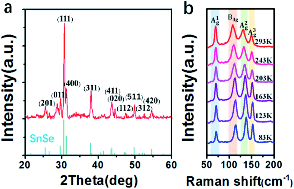 | ||
| Fig. 2 (a) XRD patterns of the SnSe film and the standard XRD patterns (ICDS: 89-0232) of SnSe. (b) Raman spectra of the SnSe film at different temperatures. | ||
In order to characterize the vibration modes of the lattice and the phase components in the samples, Raman spectroscopy of the SnSe films at different temperatures were investigated. As shown in Fig. 2(b), the spectra reveal four main vibrational modes at 70 cm−1, 107 cm−1, 130 cm−1 and 150 cm−1, in which the peak at 107 cm−1 belongs to the B3g phonon mode and the other three belong to Ag phonon modes. Ag and B3g are two rigid shear modes of a layer with respect to its neighbors in the b and c directions, respectively, which are the characteristic planar vibration modes of the lattice.26 All the observed vibrational modes agree well with the characteristic modes of orthorhombic structured SnSe crystals, which is stable at ambient conditions.27 As the temperature decreases, the Raman peaks become sharper and slightly blue-shifted, which are caused by lower thermal disturbance and reduction of stress at lower temperatures.
Then the TE properties of the polycrystalline SnSe films synthesized by single-mode MPCVD were investigated. As we know, the efficiency of TE materials is usually measured by TE power factor (S2σ) and a dimensionless figure of merit ZT = S2σT/(κL + κe), where S is the Seebeck coefficient, σ the electrical conductivity, T the temperature, and κL and κe the photonic and electronic contributions to the thermal conductivity, respectively. As shown in Fig. 3(a), the maximal Seebeck coefficient of our SnSe thin films occurs at 600 K, which is 627.7 μV K−1 and comparable to those of high-quality SnSe crystalline bulks.8,9,28 As the temperature increases, the electrical conductivity of the SnSe films first decreases then increases between 9.3 S cm−1 and 19.2 S cm−1 (Fig. 3(b)), while the thermal conductivity keeps decreasing from 0.92 to 0.58 W m−1 K−1, similar to the results observed in crystalline SnSe bulks.29 As a result, the TE power factor of the SnSe films reached up to 3.98 μW cm−1 K−2 at 600 K, which is at least one order of magnitude higher than that of the SnSe films reported by Burton et al. very recently,13 higher than that of single crystalline SnSe bulks measured along the b-axis in the moderate temperature range (500–650 K),9 and comparable to the highest reported value of SnSe thin films at 550 K.16 Furthermore, the ZT value of the MPCVD synthesized SnSe films reached maximal value of 0.335 at 600 K, which is higher than those of the SnSe films prepared by other sophisticated methods such as pulsed laser deposition,17 and comparable to those of the crystalline SnSe bulks.30–33
 | ||
| Fig. 3 Thermoelectric properties of the SnSe films as a function of temperature. (a) Seebeck coefficient. (b) Electrical conductivity. (c) Total thermal conductivity. (d) Power factors. (e) ZT values. | ||
4. Conclusions
In this work, we demonstrated a rapid and catalyst-free synthesis of SnSe thin films by single-mode MPCVD, extending the types of materials grown by MPCVD from traditional carbon-related materials to the IV–VI compounds. The grown films were composed of nanoscale SnSe polycrystals and exhibited high performance thermoelectric properties. The results may be useful for the investigation of MPCVD-grown new types of materials such as thermoelectric IV–VI compounds and the application of these materials.Conflicts of interest
There are no conflicts to declare.Acknowledgements
This work was supported by National Key R&D Program of China through Grant No. 2017YFB0405702 and by the Natural Science Foundation of China (NSFC) through Grant No. 51672179.References
- V. R. M. Reddy, S. Gedi, B. Pejjai and C. Park, J. Mater. Sci.: Mater. Electron., 2016, 27(6), 5491–5508 CrossRef.
- R. Guo, X. Wang, Y. Kuang and B. Huang, Phys. Rev. B: Condens. Matter Mater. Phys., 2015, 92(11), 115202 CrossRef.
- X. Zhou, Q. Zhang, L. Gan, H. Li, J. Xiong and T. Zhai, Adv. Sci., 2016, 3(12), 1600177 CrossRef PubMed.
- S. Li, X. Li, Z. Ren and Q. Zhang, J. Mater. Chem. A, 2018, 6(6), 2432–2448 RSC.
- J. Lu, L. Guo, G. Xiang, Y. Nie and X. Zhang, J. Electron. Mater., 2019, 1–7 Search PubMed.
- X. Cai, J. Luo, X. Zhang and G. Xiang, Mater. Res. Express, 2018, 5(3), 035013 CrossRef.
- Q. Ma, X. Zhang, D. Yang and G. Xiang, Superlattices Microstruct., 2019, 125, 365–370 CrossRef CAS.
- L. D. Zhao, G. Tan, S. Hao, J. He, Y. Pei, H. Chi, H. Wang, S. Gong, H. Xu, V. P. Dravid and C. Uher, Science, 2016, 351(6269), 141–144 CrossRef CAS PubMed.
- L. D. Zhao, S. H. Lo, Y. Zhang, H. Sun, G. Tan, C. Uher, C. Wolverton, V. P. Dravid and M. G. Kanatzidis, Nature, 2014, 508(7496), 373 CrossRef CAS PubMed.
- W. Shi, M. Gao, J. Wei, J. Gao, C. Fan, E. Ashalley, H. Li and Z. Wang, Adv. Sci., 2018, 5(4), 1700602 CrossRef PubMed.
- K. J. John, B. Pradeep and E. Mathai, J. Mater. Sci., 1994, 29(6), 1581–1583 CrossRef CAS.
- R. Indirajith, T. P. Srinivasan, K. Ramamurthi and R. Gopalakrishnan, Curr. Appl. Phys., 2010, 10(6), 1402–1406 CrossRef.
- M. R. Burton, T. Liu, J. McGettrick, S. Mehraban, J. Baker, A. Pockett, T. Watson, O. Fenwick and M. J. Carnie, Adv. Mater., 2018, 30(31), 1801357 CrossRef PubMed.
- B. Subramanian, T. Mahalingam, C. Sanjeeviraja, M. Jayachandran and M. J. Chockalingam, Thin Solid Films, 1999, 357(2), 119–124 CrossRef CAS.
- V. E. Drozd, I. O. Nikiforova, V. B. Bogevolnov, A. M. Yafyasov, E. O. Filatova and D. Papazoglou, J. Phys. D: Appl. Phys., 2009, 42(12), 125306 CrossRef.
- S. H. Heo, S. Jo, H. S. Kim, G. Choi, J. Y. Song, J. Y. Kang, N. J. Park, H. W. Ban, F. Kim, H. Jeong and J. Jung, Nat. Commun., 2019, 10(1), 864 CrossRef PubMed.
- S. Saini, P. Mele and A. Tiwari, J. Phys. Chem. Solids, 2019, 129, 347–353 CrossRef CAS.
- T. S. Yang, J. Y. Lai, C. L. Cheng and M. S. Wong, Diamond Relat. Mater., 2001, 10(12), 2161–2166 CrossRef CAS.
- C. S. Yan, Y. K. Vohra, H. K. Mao and R. J. Hemley, Proc. Natl. Acad. Sci. U. S. A., 2002, 99(20), 12523–12525 CrossRef CAS PubMed.
- Y. Kim, W. Song, S. Y. Lee, C. Jeon, W. Jung, M. Kim and C. Y. Park, Appl. Phys. Lett., 2011, 98(26), 263106 CrossRef CAS PubMed.
- J. Dong, Z. Yao, T. Yang, L. Jiang and C. Shen, Sci. Rep., 2013, 3, 1733 CrossRef.
- W. L. Wang, X. D. Bai, Z. Xu, S. Liu and E. G. Wang, Chem. Phys. Lett., 2006, 419(1–3), 81–85 CrossRef CAS.
- Y. Y. Wang, G. Y. Tang, F. A. M. Koeck, B. Brown, J. M. Garguilo and R. J. Nemanich, Diamond Relat. Mater., 2004, 13(4–8), 1287–1291 CrossRef CAS.
- D. Zhong, S. Liu, G. Zhang and E. G. Wang, J. Appl. Phys., 2001, 89(11), 5939–5943 CrossRef CAS.
- D. X. Shi, X. F. Zhang, L. Yuan, Y. S. Gu, Y. P. Zhang, Z. J. Duan, X. R. Chang, Z. Z. Tian and N. X. Chen, Appl. Surf. Sci., 1999, 148(1–2), 50–55 CrossRef CAS.
- S. Zhao, H. Wang, Y. Zhou, L. Liao, Y. Jiang, X. Yang, G. Chen, M. Lin, Y. Wang, H. Peng and Z. Liu, Nano Res., 2015, 8(1), 288–295 CrossRef CAS.
- H. R. Chandrasekhar, R. G. Humphreys, U. Zwick and M. Cardona, Phys. Rev. B: Solid State, 1977, 15(4), 2177–2183 CrossRef CAS.
- C. L. Chen, H. Wang, Y. Y. Chen, T. Day and G. J. Snyder, J. Mater. Chem. A, 2014, 2(29), 11171–11176 RSC.
- P. C. Wei, S. Bhattacharya, J. He, S. Neeleshwar, R. Podila, Y. Y. Chen and A. M. Rao, Nature, 2016, 539(7627), E1 CrossRef CAS PubMed.
- S. Sassi, C. Candolfi, J. B. Vaney, V. Ohorodniichuk, P. Masschelein, A. Dauscher and B. Lenoir, Appl. Phys. Lett., 2014, 104(21), 212105 CrossRef.
- Y. Li, F. Li, J. Dong, Z. Ge, F. Kang, J. He, H. Du, B. Li and J. F. Li, J. Mater. Chem. C, 2016, 4(10), 2047–2055 RSC.
- Y. Li, X. Shi, D. Ren, J. Chen and L. Chen, Energies, 2015, 8(7), 6275–6285 CrossRef CAS.
- J. M. Ferreiro, D. E. Diaz-Droguett, D. Celentano, J. S. Reparaz, C. S. Torres, S. Ganguli and T. Luo, Appl. Therm. Eng., 2017, 111, 1426–1432 CrossRef.
| This journal is © The Royal Society of Chemistry 2020 |