DOI:
10.1039/D0RA01073A
(Paper)
RSC Adv., 2020,
10, 14733-14745
A comparative study on the evolution of the interface chemistry and electrical performance of ALD-driven HfxTiyAlzO nanolaminates
Received
4th February 2020
, Accepted 25th March 2020
First published on 14th April 2020
Abstract
In this work, a series of ternary HfTiO and TiAlO films and quaternary HfTiAlO films prepared with different stoichiometric ratios via atomic layer deposition (ALD) were deposited on Si substrates. The interfacial properties, band alignments, and electrical characteristics were analyzed to evaluate the electrical performance of the corresponding metal–oxide–semiconductor (MOS) capacitors. Based on the characterization data, it can be noted that the permittivity of HfTiO increases on increasing the Ti content, while the deterioration of the film quality leads to an increased leakage current. For TiAlO, as the Al content increased gradually, the interface quality improved, but the corresponding permittivity was sacrificed. As for HfTiAlO, the addition of Ti and Al jointly in HfO2 could improve the interface performance, enlarge the energy band offset, enhance the dielectric constant, and reduce the leakage current simultaneously. The interfacial analysis and electrical characterization demonstrated that HfTiAlO with an ALD cycle ratio of Hf![[thin space (1/6-em)]](https://www.rsc.org/images/entities/char_2009.gif) :Ti:Al = 6:1:1 had the most excellent film quality, interface performance and electrical properties, including a larger dielectric constant of 28.8, a larger conduction band offset with Si of 2.47 eV, and the lowest leakage current density of 1.11 × 10⁻⁵ A cm−2.
:Ti:Al = 6:1:1 had the most excellent film quality, interface performance and electrical properties, including a larger dielectric constant of 28.8, a larger conduction band offset with Si of 2.47 eV, and the lowest leakage current density of 1.11 × 10⁻⁵ A cm−2.
1. Introduction
With the development of semiconductor integrated circuits, the integration and performance of chips has been continuously improving. However, with the reduction in the characteristic size of the devices, the gate leakage density increases exponentially with the thickness of the gate dielectric films, which will result in the diffusion of foreign ions and generate unacceptable direct tunneling leakage currents, further resulting in the degradation of the device performance and seriously affecting the reliability of the MOS devices. To resolve this problem, high-k dielectric materials have been introduced to replace SiO2.1–4 Among them, HfO2 has attracted much attention due to its excellent performance. HfO2 has a high dielectric constant (∼25), wide band gap (∼5.8 eV), thermally stable contact with Si, and compatibility with a metal gate.3 However, HfO2 also has many shortcomings, such as a lower crystallization temperature (600 °C), a large amount of negative charges in the film, and moderate dielectric constants, which limit further device scaling.5 Thus, the modification of HfO2 is still a continuing area of research. In order to improve the performance of HfO2, researchers have tried to dope other elements, such as Al, Ti, N, and Si, into HfO2 to obtain Hf-based high-k gate dielectrics.5,6 It is found that the doping of new elements can only partially improve the characteristics of HfO2. The introduction of new elements also introduced some new problems. For example, Al and Si incorporation can reduce the leakage current of HfO2 but does not increase the dielectric constant.7 The addition of TiO2 in HfO2 can significantly increase the dielectric constant but leads to serious deterioration in the interface quality.8
Presently, some researchers have also tried to incorporate two or more complementary elements into HfO2 simultaneously. Li et al. successfully fabricated HfTiTaO gate dielectrics by radio frequency (rf) sputter-deposition and physical vapor deposition (PVD) technology, respectively, which improved the performance by doping Ti and Ta into HfO2.9,10 Lu et al. doped Ti and Al in the HfO2 cubic structure on a Si substrate using sputtering technology and obtained an increase in the dielectric constant and an acceptable barrier height.11 These previous studies have focused mainly on the effect of the Ti content on the electrical properties of Hf-based MOS devices. However, few systematic studies have explored the effect of the doping ratio of Ti, Ta, or Al into HfO2 on the relationship between the interfacial properties, band offset and the electrical characteristics. In addition, considering the decreasing trend in device size, PVD and sputtering technology cannot meet the demand for the fabrication of ultrathin dielectric films for semiconductor devices. In comparison, atomic layer deposition (ALD) technology has outstanding advantages in obtaining high-k films with high dielectric quality as well as accurate and controllable thicknesses.12 Thus, ALD has developed into a more popular technology for preparing ultrathin gate dielectric films in recent years.13,14
Based on the above analysis, in this work, ternary oxide films, HfTiO (HTO) and TiAlO (TAO), and a quaternary oxide film, HfTiAlO (HTAO), were prepared with different doping ratios of each element by ALD technology. The effect of the doping ratio on their interfacial properties, band offset and electrical characteristics, as well as the relationship between these properties were systematically investigated and analyzed.
2. Experimental
2.1 Preparation of samples
n-Doped Si (100) wafers with the resistance of 10–20 Ω were chosen as substrates. Before the deposition of films, the Si wafers were cleaned by a standard RCA cleaning method. Laminate films, including HTO, TAO, and HTAO, were deposited by atomic layer deposition (ALD) technology in an ALD chamber (LabNano™ 9100, ENSURE NANOTECH). Tetrakis(dimethylamino)hafnium (TDMAH), tetrakis(dimethylamino)titanium (TDMAT), and trimethylaluminum (TMA) were chosen as the metal precursors for HfO2, TiO2, and Al2O3, respectively. H2O was used as the oxidant for all metal oxides. TDMAH and TDMAT were heated to 80 °C and H2O and TMA were kept at room temperature. All HTO, TAO, and HTAO films were deposited with a N2 flow rate of 20 SCCM at 150 °C. HfO2 was obtained by alternate TDMAH (0.2 s)/Ar (60 s)/H2O (0.2 s)/Ar (60 s) pulses for each self-limiting cycle. Similarly, TiO2 and Al2O3 were prepared by TDMAT (0.2 s)/Ar (20 s)/H2O (0.2 s)/Ar (30 s), and TMA (0.2 s)/Ar (20 s)/H2O (0.2 s)/Ar (20 s) pulses, respectively. The corresponding deposition rates of the TiO2, Al2O3 and HfO2 films were 0.55 Å per cycle, 1.2 Å per cycle, and 0.9 Å per cycle, respectively. All the laminate films with different doping concentrations were controlled by adjusting the ALD cycle ratio: (x(HfO2) + y(TiO2) + z(Al2O3)) × n, according to the difference in the ratio of ALD cycles. All samples were denoted with different symbols. As listed in Table 1, the HTO films were assigned as S1–S6, the TAO were assigned as S1′–S6′, and the HTAO were named as S1′′–S5′′, respectively. About 9 nm thick laminate films for the MOS devices and 4 nm thick laminate films for X-ray photoelectron spectroscopy (XPS) tests were prepared on Si wafers by ALD technology. Additionally, to obtain optical band gap values (Eg), about 40 nm thick laminate films were deposited on quartz substrates for ultraviolet-visible spectroscopy (UV-vis) measurements. The thickness of all the laminate films were examined by spectroscopic ellipsometry (SC630, SANCO Co, Shanghai) and obtained by fitting the Cauchy dispersion model. In order to investigate the effect of the doping amount of Ti and Al on the electrical properties of HfO2, a set of Si–MOS devices was fabricated. About 200 nm thick Al top electrodes were deposited on gate dielectric films through a shadow mask with an area of 3.14 × 10⁻⁴ cm2 by direct current (DC) magnetron sputtering deposition technology. Additionally, to resolve the ohm contact problem, about 200 nm thick Al back electrodes were also deposited on the Si back surfaces after stripping the surface oxides. The structure of the Si–MOS device is sketched in Fig. 1.
Table 1 Summary of all samples with different precursor cycle ratio
| HfTiO |
Precursor ratio of Hf(x):Ti(y) |
TiAlO |
Precursor ratio of Ti(y):Al(z) |
HfTiAlO |
Precursor ratio of Hf(x):Ti(y):Al(z) |
| S1 |
1:0 |
S1′ |
0:1 |
S1′′ |
1:1:1 |
| S2 |
6:1 |
S2′ |
1:1 |
S2′′ |
2:1:1 |
| S3 |
4:1 |
S3′ |
2:1 |
S3′′ |
4:1:1 |
| S4 |
2:1 |
S4′ |
4:1 |
S4′′ |
6:1:1 |
| S5 |
1:1 |
S5′ |
6:1 |
S5′′ |
8:1:1 |
| S6 |
0:1 |
S6′ |
1:0 |
|
|
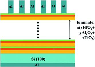 |
| | Fig. 1 A diagram of the Si–MOS device. | |
2.2 Sample characterization
All samples were characterized to determine their interfacial chemical composition, band alignment, and electrical properties, respectively. Ex situ XPS measurements were carried out on an ESCALAB 250Xi system to characterize the interfacial chemical states between the films and Si substrate. For XPS, the radiation source was equipped with an Al Kα radiation source (Eg = 1486.6 eV). All the XPS spectra were detected at a take-off angle of 45° and with an energy interval of 0.1 eV by means of a hemispherical analyzer and the pass energy was 20 eV. The absorption spectra of all films over the range of 300–900 nm were measured at room temperature using the SHIMADZU UV-2550 ultraviolet-visible spectrometer (UV-vis). The band gap values of films were obtained from the absorption spectrum by optical methods. The DC capacitance–voltage (C–V) and leakage current–voltage (I–V) characteristics of the MOS devices were measured using an Agilent B1500A semiconductor parameter analyzer combined with a Cascade Probe Station at room temperature and in a shielding dark case.
3. Results and discussion
3.1 HTO capacitors
3.1.1 Interface chemistry characterization. Fig. 2(a) shows the core-level XPS survey spectra for S1–S6. It is obvious that from S1 to S6, the intensity of the Hf peaks gradually weakened and the intensity of each Ti peak was gradually enhanced with the change of the ALD cycle ratio of Hf:Ti. The changes in the interface chemical composition could be obtained by determining the Si 2p core-level spectra, which are fitted with seven peaks as exhibited in Fig. 2(b). The Si 2p doublet peaks (resulting from a spin–orbit splitting of 0.5 eV between 2p1/2 and 2p3/2) are located at 99.3 eV and 99.8 eV, which are fitted with a full width at half maximum (FWHM) of about 0.6 eV. The other five peaks related to the intrinsic oxides of Si (i.e., Si1+, Si2+, Si3+, and Si4+) and silicate (Si*) were fit with a FWHM of about 1.15 eV and are located at 100.3 eV, 100.95 eV, 101.8 eV, 102.6 eV, and 103.2 eV, arranged by binding energy from low to high, respectively. In order to obtain the change of chemical composition at the interfacial layer more clearly, the relative peak area percentages of silicate and four Si oxides were also calculated and are listed in Table 2. It can be seen that the relative peak area percentages of silicate in S1–S6 are 16.93%, 20.97%, 27.33%, 33.31%, 33.22% and 27.63%, respectively. It is observed that the silicate content for S1 in the interfacial layer between the HfO2 film and Si substrate is minimized. In contrast, for S6, the silicate composition in the interface layer between TiO2 film and Si substrate is higher. For S2–S5, the silicate component rises with increasing Ti content in the HTO films, which is consistent with Ye et al.15. Ye et al. found that the interface quality would deteriorate with increasing Ti content, which is due to the increase of silicate.15 So, it can be summarized that TiO2 can more easily react with Si than HfO2 and form more silicate during deposition in the ALD chamber. The incorporation of Ti into HfO2 is detrimental to the interface quality between the HTO film and Si wafer.
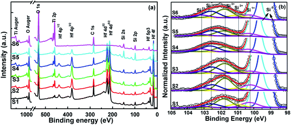 |
| | Fig. 2 (a) Core level XPS spectra for all compositions and (b) Si 2p XPS spectra analysis of S1–S6. | |
Table 2 The relative peak area percentages of Si1+, Si2+, Si3+, Si4+, Si* in Si 2p peaks for S1–S6
| |
Si1+ (%) |
Si2+ (%) |
Si3+ (%) |
Si4+ (%) |
Si* (%) |
| S1 |
23.06 |
14.89 |
38.95 |
6.16 |
16.93 |
| S2 |
20.18 |
8.15 |
41.02 |
9.68 |
20.97 |
| S3 |
10.12 |
10.63 |
42.63 |
9.29 |
27.33 |
| S4 |
15.84 |
6.38 |
28.52 |
15.95 |
33.31 |
| S5 |
17.22 |
9.09 |
32.56 |
7.91 |
33.22 |
| S6 |
13.35 |
10.92 |
37.46 |
10.63 |
27.63 |
3.1.2 Band alignment. It is well known that the k values of gate dielectrics are inversely related to the band gap (Eg) values. The higher the k values are, the greater the physical thickness of the gate dielectric material is, so as to effectively inhibit the direct tunneling current. However, more often than not, the corresponding band gap value is smaller. So, the Schottky emission induced by thermionic emission usually takes place through the valence or conduction band edge. To limit the leakage current, the candidate high-k dielectrics should satisfy the requirement that both the valence band offset (VBO) and the conduction band offset (CBO) are larger than 1 eV. So, the band alignment analysis determined by the energy of the VBO and CBO plays a critical role in the evaluation of high-k material performance. The energy band gaps edges are measured through the UV-vis absorption spectrum and attained using the linear extrapolation method. In order to obtain the VBO values for high-k gate dielectric films, the valence band offset (ΔEv) values are determined by Kraut's method as shown in the relation below:16| | |
ΔEv(high-k–Si) = Ev(high-k) − Ev(Si)
| (1) |
The Ev values are also attained using the linear extrapolation. At last, the conduction band offset (ΔEc) values can be obtained by the equation below:| | |
ΔEc(high-k–Si) = Eg(high-k) − ΔEv(high-k–Si) − Eg(Si)
| (2) |
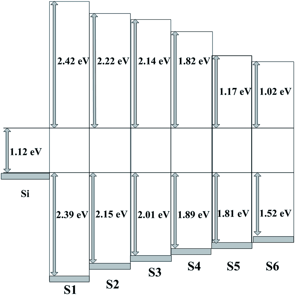
Based on ΔEv and ΔEc, the schematic band diagram of the high-k/Si stack can be determined.Using the approach described above, the Eg and Ev for S1–S6 are depicted in Fig. 3(a) and (b). The Eg of HfO2 and TiO2 is 5.93 eV and 3.66 eV, respectively. The Eg of S2–S5, i.e., the HTO films, is found to smaller than that of HfO2 and larger than that of TiO2, and decreases from 5.49 eV to 4.10 eV with increasing Ti content. The ΔEv values of S1–S6 show the same trend, with the values of 2.39, 2.15, 2.01, 1.89, 1.81, and 1.56 eV, respectively. The decreased conduction band offsets with increasing Ti content are observed in Fig. 4. As displayed in Fig. 4, the extracted ΔEc of S1–S6 are 2.42, 2.22, 2.14, 1.82, 1.17, and 1.02 eV, respectively. These are consistent with our previous research findings and Ye's findings obtained by a magnetron sputtering method.15,17 As reported in the previous literature, the Eg of TiO2 is dominated by Ti 3d and O 2s or O 2p states, as well as Hf 5d and O 2p states that contribute to the Eg of HfO2.18,19 Because the energy of the Hf 5d state is above that of Ti 3d, the CB edge and the band gap of HfTiO are reduced with increasing Ti content.
 |
| | Fig. 3 The difference between (a) the band gap and (b) the VBM for S1–S6. | |
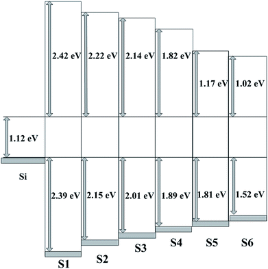 |
| | Fig. 4 The schematic band diagram of S1–S6. | |
3.1.3 Electrical characterization. Double sweep C–V measurements for all samples were taken at high frequency (1 MHz) along the clockwise direction. For high-k/Si stacks, there are four types of oxide charges on the side of the high-k dielectrics. According to their distribution, they are also called fixed oxide charges, mobile ion charges, oxide trapped charges, and interface trapped charges, respectively. These defective charges in the oxide film will lead to the deviation between the measured CV curves in the experiment and the ideal CV curves. Among them, the fixed oxide charges and the mobile ion charges will cause the CV curve to drift along the voltage axis; the oxide trapped charges can cause hysteresis of the CV curve; and the interface trapped charges will bring about CV distortion. According to the accumulated capacitance (Cacc), the corresponding permittivity (k) values can be extracted. From the deformation of the CV curves, the flat band voltage (Vfb) and hysteresis of the flat band voltage (ΔVfb) can be calculated. Furthermore, the fixed charge density (Qox), the trapped oxide charge density (Qbt) can be obtained. So, from the CV curves, we can extract some electrical parameters to evaluate the quality of the high-k dielectric thin films and the electrical properties of the MOS capacitors.The bias voltage shift of the CV curve is mainly due to the fixed oxide charges and the native defect charges in the oxides near the interface region. When the fixed oxide charges are positive, the corresponding CV curve moves in the direction of the negative voltage; whereas if the fixed oxide charges are negative, the CV curve will move toward the positive voltage. Qox can be obtained using the following formula:20–22
| | |
Qox = −Cacc(Vfb − Φms)/Aq
| (3) |
in which
Φms is the difference in work function between the aluminum electrode and Si substrate,
A is the aluminum metal electrode area, and Δ
Vfb, depending on the bias, is ascribed to the trapped charges existing in the oxide and interface layer. These trapped oxide charges include the hole trapping state and the electron trapping state, which can trap holes and electrons in the oxide film, respectively, and make them charged positively and negatively. Thus, in the process of a bi-directional sweep voltage, the bias voltage hysteresis of the CV curve occurred. So, the density of trapped oxide charges can be obtained by the formula:
20–22
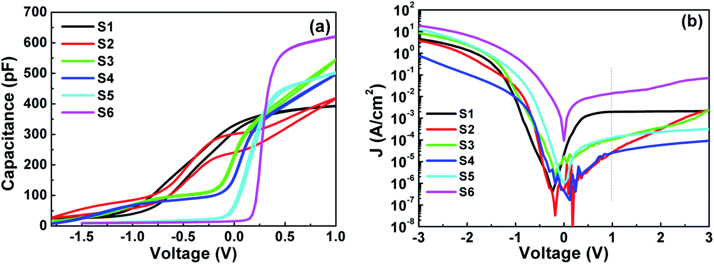
Fig. 5(a) shows the C–V curves of Al/HTO/Si–MOS capacitors with different Ti doping content. It can be seen that the Cacc of S1, i.e., HfO2, is the minimum, whereas, that of S6, i.e., TiO2, is the maximum. As for HTO, the Cacc values are larger than that of HfO2 and smaller than that of TiO2, and rise with increasing Ti content. The corresponding k values extracted from Cacc are 13.9, 16.4, 19.6, 22.1, 23.1, and 29.5, respectively. The k values increase with increasing Ti content and are consistent with those reported in the literature.15,17 For S1, there is a left flatland shift in the CV curve, which is due to the positive trapped oxide charges or positive intrinsic defects existing in the HfO2 film and/or in the HfO2/Si interface layer.20,22 For S6, a right flatland shift in the CV curve is observed. On one hand, it is because of the difference in work function between the gate dielectric film and Si substrate; on the other hand, it is due to the negative trapped oxide charges or negative intrinsic defects existing in the TiO2 film and/or in the TiO2/Si interface layer.20,22 As for S2–S5, after doping TiO2 into HfO2, there is a great negative shift in the Vfb as compared to HfO2 and TiO2. The Qox of all samples can be calculated and is listed in Table 3 they are 2.08 × 10¹², 1.74 × 10¹², −5.48 × 10¹¹, −3.79 × 10¹¹, −7.22 × 10¹¹, −1.84 × 1012 cm−2, respectively. It can be observed that the Qox values for the HTO samples vary from positive to negative with increasing Ti content. It may be due to the increase of the positive trapped oxide charges or negative intrinsic defects. These charges may originate from the oxygen vacancies in oxides caused by dangling bonds on the Si surface, which originates from the lack of oxygen atoms during the gate dielectric film deposition.20,22 A flatland shift along the positive voltage direction is observed with increasing Ti content, which is attributed to an increase in the positive oxide charges in the films near the interface layers.20,22
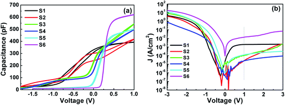 |
| | Fig. 5 (a) Capacitance–voltage (C–V) characteristics. (b) Leakage current density–voltage (J–V) characteristics for S1–S6. | |
Table 3 The electrical parameters extracted for S1–S6
| HfTiO |
Cacc (F) |
εhk |
Cfb (pF) |
Vfb (V) |
ΔVfb (V) |
Qox (cm−2) |
Qbt (cm−2) |
J (A cm−2) |
| S1 |
2.39 × 10⁻¹⁰ |
13.9 |
1.30 × 10⁻¹⁰ |
0.11 |
0.09 |
2.08 × 10¹² |
−5.51 × 10¹² |
2.07 × 10⁻³ |
| S2 |
4.11 × 10⁻¹⁰ |
16.4 |
1.65 × 10⁻¹⁰ |
−0.54 |
0.08 |
1.74 × 10¹² |
−4.73 × 10¹² |
3.06 × 10⁻⁵ |
| S3 |
4.73 × 10⁻¹⁰ |
19.6 |
1.65 × 10⁻¹⁰ |
−0.07 |
— |
−5.48 × 10¹¹ |
— |
1.11 × 10⁻⁴ |
| S4 |
5.19 × 10⁻¹⁰ |
22.1 |
1.70 × 10⁻¹⁰ |
0.01 |
— |
−3.79 × 10¹¹ |
— |
2.65 × 10⁻⁵ |
| S5 |
5.37 × 10⁻¹⁰ |
23.1 |
1.73 × 10⁻¹⁰ |
0.07 |
— |
−7.22 × 10¹¹ |
— |
1.28 × 10⁻⁴ |
| S6 |
6.41 × 10⁻¹⁰ |
29.5 |
1.90 × 10⁻¹⁰ |
0.255 |
— |
−1.84 × 10¹² |
— |
1.53 × 10⁻² |
Additionally, it can be observed that there is obvious hysteresis and stretching in the depletion region for S1; while for S6, there is almost no hysteresis and no stretching in the depletion region. Compared with S1 and S6, the CV curves of S2–S5 changed significantly after doping TiO2 into HfO2 to form HTO samples. When the Hf content is higher, such as in S2, the ΔVfb increases and the stretching in the depletion region and distortion also worsen. Interestingly, as the content of Ti increases gradually, the voltage hysteresis is quickly eliminated. The density of border trapped charges causing hysteresis is calculated and listed in Table 3. The Qbt for HfO2 (S1) is −5.51 × 1011 cm−2 and that for TiO2 (S6) is almost 0. Also, the Qbt for other HTO are 0, except for S2, which corresponds to the maximum Hf content.
As depicted in Fig. 5(b), the leakage current densities from the gate voltage (J–V) curves for all samples were measured by sweeping the voltage from −3 V to +3 V, and the corresponding leakage current densities (J) at +1 V were extracted to compare. As listed in Table 3, the J values of S1–S6 are 2.07 × 10⁻³, 3.06 × 10⁻⁵, 1.11 × 10⁻⁴, 2.65 × 10⁻⁵, 1.28 × 10⁻⁴, and 1.53 × 10⁻² A cm−2, respectively. Combined with XPS fitting results, band alignment and electrical analysis, this indicates that S5 (ALD cycle ratio of Hf:Ti = 1:1) presents ideal CV characteristics with the smallest flat voltage and almost no hysteresis, and possesses excellent film properties with the least defect charges. However, the poor interface properties and smaller conduction band offset inhibit the improvement of the electrical properties. S5 has a modest dielectric constant (∼23.1), but the leakage current (∼1.28 × 10⁻⁴ A cm−2) is also larger. It is obvious that doping Ti into HfO2 cannot simultaneously improve both: the cost of improving the dielectric constant is an increase in the leakage current.
3.2 TAO capacitors
Based on the interface analysis for HTO, it can be demonstrated that TiO2 is more susceptible to reaction on a Si substrate and forms more silicate during deposition as compared with HfO2. To inhibit the diffusion between TiO2 and the Si substrate and suppress the leakage current, Al2O3, which possesses good passivation properties, was doped into TiO2 to form a TAO laminated film.
3.2.1 Interface characterization. In Fig. 6(a), the survey spectra for S1′–S6′ display the intensity of Ti peaks decreasing and the intensity of Al peaks increasing with the change of the ALD cycle ratio of Ti:Al from 0:1 to 1:0. Fig. 6(b) shows the Si 2p XPS core level of TAO/Si. Similarly to the HTO XPS analysis above, Si–O bonds are deconvoluted into four oxides and silicate peaks. The relative peak area percentages of silicate and the four Si oxides are further calculated and listed in Table 4. It can be seen that the relative peak area percentages of silicate for S1′–S6′ are 7.90%, 16.63%, 21.06%, 26.88%, 26.71% and 27.63%, respectively. It is obvious that for S1′, there is only a small amount of silicate at the interface layer. By contrast, for S6′, there is a lot of silicate in the interface layer. For S2′–S5′, the silicate in the interface layer decreases with increasing Al content in TAO. It is not difficult to deduce that the incorporation of Al2O3, which has excellent chemical stability and passivation effects, effectively suppresses the oxygen diffusion downward into the Si substrate, thus reducing the generation of silicate.23–25 This is in agreement with our previous research on HAO/Si gate stacks.26,27
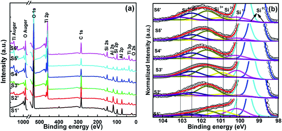 |
| | Fig. 6 (a) Core level XPS spectra for all compositions and (b) Si 2p XPS spectra analysis of S1′–S6′. | |
Table 4 The relative peak area percentages of Si1+, Si2+, Si3+, Si4+, Si* in Si 2p peaks for S1′–S6′
| |
Si1+ (%) |
Si2+ (%) |
Si3+ (%) |
Si4+ (%) |
Si* (%) |
| S1′ |
43.37 |
22.05 |
21.69 |
4.99 |
7.90 |
| S2′ |
6.00 |
14.31 |
51.00 |
12.06 |
16.63 |
| S3′ |
20.61 |
13.88 |
39.52 |
4.93 |
21.06 |
| S4′ |
16.62 |
6.76 |
41.38 |
8.36 |
26.88 |
| S5′ |
11.81 |
5.71 |
46.17 |
9.60 |
26.71 |
| S6′ |
13.35 |
10.92 |
37.46 |
10.64 |
27.63 |
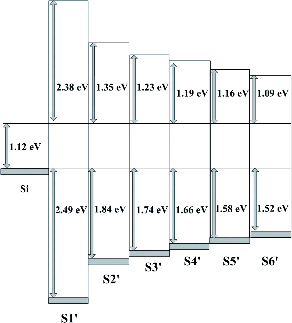
3.2.2 Band alignment. The band alignment of the TAO film with the Si substrate was determined using the method described above for the analysis of the HTO film. Fig. 7(a) shows the experimental data on the band gaps for S1′–S6′. The Eg estimated for pure Al2O3 and TiO2 are about 5.99 eV and 3.73 eV, respectively. The Eg of the TAO film gradually increases as the Ti content decreases in the range of 3.86–4.31 eV. The results are in agreement with the values reported in previous studies.28–30 The ΔEv for S1′–S6′ as a function of Ti content are shown in Fig. 7(b). This reveals that there is a gradual increase in ΔEv with decreasing Ti content. The ΔEv value of TAO is closer to that of TiO2 and seems to be dominated by that of TiO2, which was observed by An et al. and Alekhin et al. for TAO on GaAs and Si, respectively.28,31 Using formula (2) above, the ΔEc for S1′–S6′ are calculated and presented in Fig. 8. It is well known that the conduction band offset of the TiO2/Si heterojunction is below 1 eV. In this work, the ΔEc obtained for TiO2 is 0.93 eV, which is consistent with data obtained in earlier studies. The ΔEc for TAO slowly increases from 1.01 eV to 1.19 eV with the increase of Al content and is closer that of TiO2. A possible explanation for these results may be that the Al content in the TAO cannot effectively increase the ΔEc values relative to n-Si. These results can be attributed to the interfacial layer between TAO and the Si substrate that tunes the ΔEc values, as reported in the studies of An et al. and Perego et al.28,30.
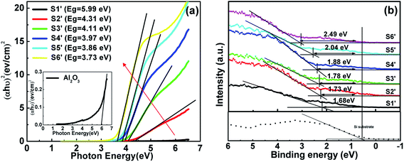 |
| | Fig. 7 The difference between (a) the band gap and (b) the VBM for S1′–S6′. | |
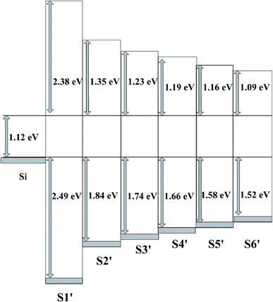 |
| | Fig. 8 The schematic band diagram of S1′–S6′. | |
3.2.3 Electrical properties. The electrical properties of Al/TAO/Si stacks are characterized by C–V and J–V measurements as exhibited in Fig. 9(a) and (b). It can be seen that the incorporation of Al2O3 modulates the electrical properties of TiO2. The Cacc of S2′–S5′ first increases and then decreases with increasing Al content. The change of Cacc can be explained by a small amount of Al doping that improves the interfacial properties between TAO and the Si substrate and inhibits the formation of silicates, and thus enhances Cacc; however, with the increase of Al content, the effect of Al2O3 with low permittivity on TAO is more and more significant, which will lead to the decrease of Cacc. The permittivity of the TAO film is calculated from Cacc and listed in Table 5. From the bi-directional CV curves, it can be seen that the ΔVfb increases obviously after the incorporation of Al into TiO2. Taking into account the postulation mentioned in the case of HTO, it can be speculated that the trapped charges existing in the TiO2/Al2O3 laminate film lead to the increase in ΔVfb. Meanwhile, the shifts of the TAO Vfb relative to TiO2 are due to the change in the oxide charges in the TAO film near the interface layers. It can be observed that the CV curves move first to the right and then to the left, which indicates that the fixed charges in the TAO film increase first and then decrease. Additionally, with the increasing Al content in the TAO film, the upward trend in the accumulation area of the CV curves was eliminated, which symbolizes that the interface state is suppressed. From Fig. 9(b), it can be clearly seen that there was a marked decrease in the gate leakage current with the increase of Al content in the TAO film. Additionally, S2′owns the lowest leakage current density (∼7.31 × 10⁻⁶ A cm−2).
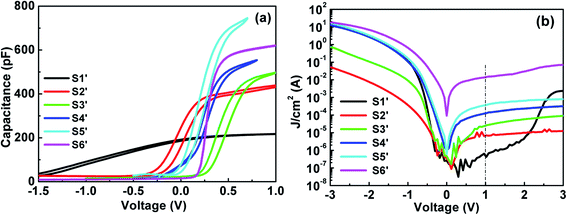 |
| | Fig. 9 (a) Capacitance–voltage (C–V) characteristics. (b) Leakage current density–voltage (J–V) characteristics for S1′–S6′. | |
Table 5 The electric parameters extracted for S1′–S6′
| TiAlO |
Cmax (pF) |
εhk |
Cfb (pF) |
Vfb (V) |
ΔVfb (V) |
Qox (cm−2) |
Nbt (cm−2) |
J (A cm−2) |
| S1′ |
2.21 × 10⁻¹⁰ |
7.2 |
1.31 × 10⁻¹⁰ |
−0.64 |
0.08 |
2.01 × 10¹² |
−3.22 × 10¹¹ |
6.03 × 10⁻⁷ |
| S2′ |
4.57 × 10⁻¹⁰ |
18.4 |
2.46 × 10⁻¹⁰ |
0.076 |
0.066 |
−7.72 × 10¹¹ |
−1.42 × 10¹² |
7.31 × 10⁻⁶ |
| S3′ |
4.76 × 10⁻¹⁰ |
19.7 |
2.14 × 10⁻¹⁰ |
0.12 |
0.093 |
−6.71 × 10¹² |
−1.51 × 10¹² |
2.39 × 10⁻⁵ |
| S4′ |
5.33 × 10⁻¹⁰ |
22.9 |
2.09 × 10⁻¹⁰ |
0.32 |
0.085 |
−4.41 × 10¹² |
−1.23 × 10¹² |
1.23 × 10⁻⁴ |
| S5′ |
7.05 × 10⁻¹⁰ |
33.8 |
1.86 × 10⁻¹⁰ |
−0.065 |
0.095 |
−4.36 × 10¹² |
−8.15 × 10¹¹ |
4.02 × 10⁻⁴ |
| S6′ |
6.50 × 10⁻¹⁰ |
29.5 |
1.90 × 10⁻¹⁰ |
0.255 |
0.01 |
−4.15 × 10¹² |
−1.28 × 10¹¹ |
1.53 × 10⁻² |
Combining the analysis results extracted from XPS, band alignment, and electrical characteristics, it can be concluded that the incorporation of Al2O3 in TiO2 can reduce the generation of SiO2 and silicate, improve the quality of the interface and TAO films, increase Eg and ΔEc relative to Si, and reduce the gate leakage current, but at the expense of permittivity. In this work, S2′ (precursor ratio of T:Al = 1:1) exhibits excellent interface and film properties, the smallest leakage current (∼7.31 × 10⁻⁶ A cm−2), but has a low k value (∼18.4). So, when Al is used to modulate the properties of the TiO2/Si stack, the doping amount of Al should be strictly controlled.
3.3 HTAO capacitors
The evidence presented in the preceding two sections suggests that adding TiO2 into HfO2 can increase the permittivity, but deteriorate the interface; while incorporating Al2O3 into TiO2 can improve the quality of the interface and limit the leakage current of films, but it must be at the expense of decreasing the dielectric constant. In our previous work, HAO obtained through doping Al2O3 into HfO2 had the same problems as TAO.7,26,27 So, in this section, both Al2O3 and TiO2 are incorporated into HfO2 to form a quaternary oxide, HTAO. Based on the analysis above for the TAO/Si stacks, the sample S2′with the precursor ratio of T:Al = 1:1 has excellent characteristics in the film and interface layer, and the smallest leakage current. So, in this work, the precursor ratio of T:Al was fixed at 1:1 and the number of cycles of Hf precursor was changed to obtain HTAO with a different doping ratio.
3.3.1 Interface characterization. Fig. 10(a) shows the survey spectra for S1′′–S5′′. It can be seen that the intensity of Al 2s and Ti 2p decrease gradually from S1′′ to S5′′ with increases in the ALD precursor cycle number of HfO2. Fig. 10(b) exhibits the Si 2p XPS spectra of HTAO/Si. Si 2p is deconvoluted into seven peaks following the spectra-decomposition method used in Section 3.1. What can be clearly seen in Fig. 10(b) is the changes of silicate and silica oxide content with the incorporation of Ti and Al into HfO2. The relative peak area percentages of silicate and the four Si oxides for S1′′–S5′′ are also calculated and listed in Table 6. It can be seen that the relative peak area percentages of silicate are 27.07%, 19.95%, 13.81%, 10.47%, and 23.03%, respectively. With the decrease of Ti and Al content, i.e., the increase of Hf content in HTAO, the silicate at the interfacial layer decreased first and then increased. When the ALD cyclic ratio of Hf:Al:Ti is equal to 6:1:1, the silicate is the lowest. Combining the XPS analysis results in Section 3.1, TiO2 diffuses more readily into Si than HfO2. When the ALD cyclic ratio of Ti:Al is fixed at 1:1, the increasing Hf content would inhibit the diffusion between HTAO and the Si substrate to optimize the interfacial quality. However, as the Hf content continues to increase, the Al content in HTAO is not enough to inhibit the diffusion of Hf and Ti into the Si substrate. Therefore, as the ALD cyclic ratio of Hf:Al:Ti increased to 8:1:1, the silicate and SiO2 in the interface layer increased instead.
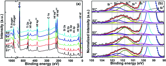 |
| | Fig. 10 (a) Core level XPS spectra for all compositions and (b) Si 2p XPS spectra analysis of S1′′–S6′′. | |
Table 6 The relative peak area percentages of Si1+, Si2+, Si3+, Si4+, Si* in Si 2p peaks for S1′′–S6′′
| |
Si1+ (%) |
Si2+ (%) |
Si3+ (%) |
Si4+ (%) |
Si* (%) |
| S1′′ |
14.85 |
9.44 |
39.53 |
9.11 |
27.07 |
| S2′′ |
15.93 |
10.77 |
40.42 |
12.93 |
19.95 |
| S3′′ |
11.04 |
7.68 |
56.33 |
11.14 |
13.81 |
| S4′′ |
12.75 |
10.52 |
57.66 |
8.60 |
10.47 |
| S5′′ |
11.11 |
11.11 |
43.07 |
11.68 |
23.03 |
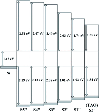
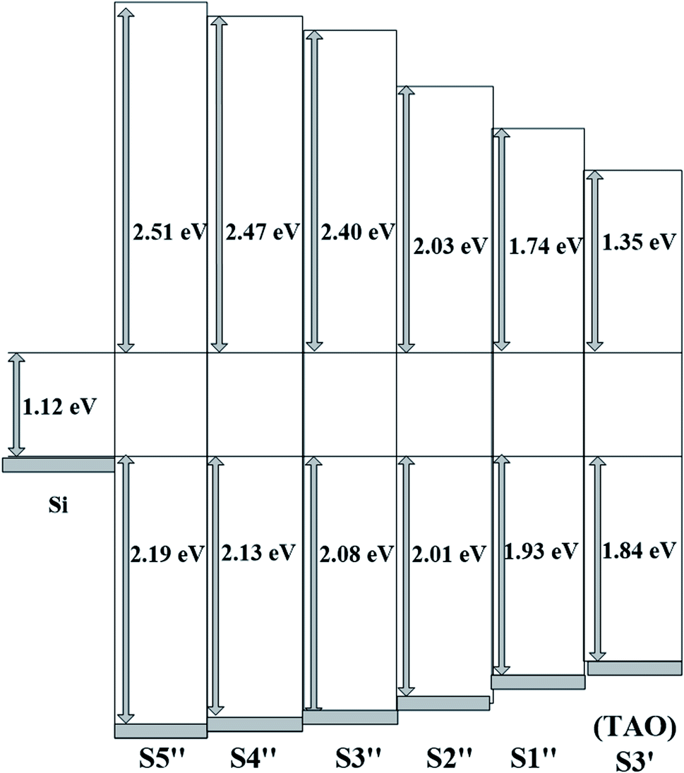
3.3.2 Band alignment. The band alignment of the HTAO film with Si substrates was determined using the method described in Section 3.1. In Fig. 11(a), the Eg of S1′′–S5′′ are 5.82, 5.72, 5.60, 5.16, and 4.79 eV, respectively. The Eg values of HTAO are smaller than those of Al2O3, but higher than TiO2, and closer to HfO2 with increasing Hf content. These results are consistent with those reported in Hf0.52Ti0.33Al0.15O by Aleklin et al.32 The ΔEv for S1′′–S5′′ as a function of Hf content are shown in Fig. 11(b). It is apparent that there is a gradual increase from 1.93 to 2.19 eV with the increase in Hf content. Following formula (2) in Section 3.1, the calculated ΔEc for S1′′–S5′′ are exhibited in Fig. 12. The CBO of HTAO/Si increases from 1.74 to 2.51 eV with the increase of Hf content. In addition, it can be seen that there was a marked increase in the CBO as the ALD cycle of the Hf precursor varies from 1 to 4; while as the ALD cycle of the Hf precursor varies from 4 to 8, the CBO exhibits a slight increase. Compared with the above XPS analysis of HTO/Si and TAO/Si, it is possible conclude that the performance of the HfO2/Si interface is better than that of the TiO2/Si interface. Thus, the appropriate increase of Hf content in the HTAO film can improve the interfacial properties. Nevertheless, with the continued increase of Hf content, the decrease in the relative composition of Al is not sufficient to inhibit the diffusion between Si and the HTAO film, which will lead to the deterioration of interface performance.
 |
| | Fig. 11 The difference between (a) the band gap and (b) the VBM for S1′′–S6′′. | |
 |
| | Fig. 12 The schematic band diagram of S1′′–S6′′. | |
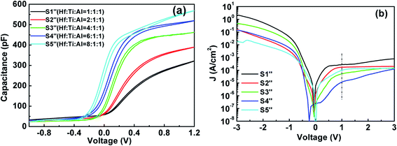
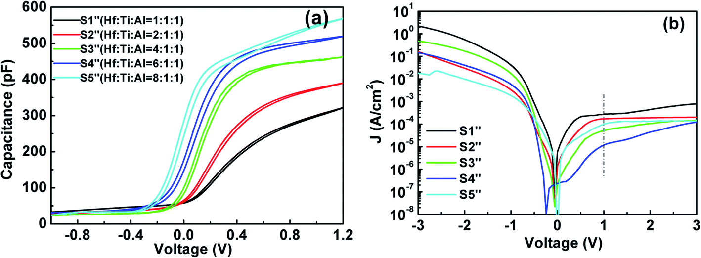
3.3.3 Electrical properties. In Fig. 13(a), the C–V curves for the Al/HTAO/Si–MOS capacitors are presented. Compared with the HTO and TAO samples, it is obvious that the shape of the C–V curves for HTAO is closer to that of an ideal C–V curve. The voltage hysteresis of all curves is very small and the values are very close around 0.03 V. Such a small hysteresis indicates that the trapped charges existing in the HTAO films and interface layers are reduced by doping Hf, Ti, and Al oxides together. From Table 7, the extracted Nbt for S1′′–S6′′ is −1.44 × 10¹¹, −1.59 × 10¹¹, −2.10 × 10¹¹, −3.06 × 10¹¹, and −3.48 × 1011 cm−2, respectively. The number of trapped charges in the quaternary oxide HTAO is one order of magnitude lower than that of the ternary oxides HTO and TAO. From our experimental results, it can be seen that for TiO2, there is almost no hysteresis in the MOS devices, so trapped charges in the TiO2 film can be ignored. Additionally, Al2O3 plays a passivation role to improve the quality of the interface layer. Therefore, doping Al2O3 and TiO2 into HfO2 can not only improve the interface quality, but also reduce the voltage hysteresis, thus reducing the number of trapped charges in the HTAO film.
 |
| | Fig. 13 (a) Capacitance–voltage (C–V) characteristics. (b) Leakage current density–voltage (J–V) characteristics for S1′′–S6′′. | |
Table 7 The electrical parameters extracted for S1′′–S6′′
| HfTiAlO |
Cmax (pF) |
εhk |
Cfb (pF) |
Vfb (V) |
ΔVfb (V) |
Qox (cm−2) |
Nbt (cm−2) |
J (A cm−2) |
| S1′′ |
3.22 × 10⁻¹⁰ |
12.8 |
1.68 × 10⁻¹⁰ |
0.33 |
0.025 |
−2.25 × 10¹² |
−1.44 × 10¹¹ |
2.76 × 10⁻⁴ |
| S2′′ |
3.90 × 10⁻¹⁰ |
17.7 |
1.75 × 10⁻¹⁰ |
0.21 |
0.022 |
−1.92 × 10¹² |
−1.59 × 10¹¹ |
1.56 × 10⁻⁴ |
| S3′′ |
4.63 × 10⁻¹⁰ |
23.9 |
1.84 × 10⁻¹⁰ |
0.083 |
0.024 |
−1.25 × 10¹² |
−2.10 × 10¹¹ |
5.03 × 10⁻⁵ |
| S4′′ |
5.20 × 10⁻¹⁰ |
28.8 |
1.98 × 10⁻¹⁰ |
0.020 |
0.031 |
−7.75 × 10¹¹ |
−3.06 × 10¹¹ |
1.11 × 10⁻⁵ |
| S5′′ |
5.69 × 10⁻¹⁰ |
35.5 |
1.97 × 10⁻¹⁰ |
−0.069 |
0.032 |
9.33 × 10¹⁰ |
−3.43 × 10¹¹ |
1.04 × 10⁻⁴ |
| S6′′ |
4.10 × 10⁻¹⁰ |
18.6 |
1.77 × 10⁻¹⁰ |
−0.028 |
0.028 |
3.19 × 101 |
−1.02 × 10¹¹ |
6.01 × 10⁻⁶ |
The deviation of the CV curve to a more positive voltage decreases with the increase of Hf content. The corresponding Vfb for S1′′–S5′′are 0.33, 0.21, 0.083, 0.020, and −0.069 V, respectively. The deviation of the CV curves is mainly due to the negative fixed oxide charges and the native defect charges in the HTAO films that decrease with increasing Hf content. The extracted Qox for S1′′–S5′′ in Table 7 are −2.25 × 10¹², −1.92 × 10¹², −1.25 × 10¹², −7.75 × 10¹¹, and −9.33 × 1010 cm−2, respectively. With the increase of Hf content, the number of oxide charges in S5′′ is about two orders of magnitude lower than that of S1′′. Moreover, Cacc increases obviously with increasing Hf content too. The permittivity for S1′′–S5′′ increases in turn and are 12.8, 17.7, 23.9, 28.8, and 35.5, respectively. These results are in good agreement with the experimental studies from Lu et al. and Alekhin et al.11,32. Combined with the preceding analysis, the relative content of Hf and Ti with a high dielectric constant increases; on the other hand, the reduction of SiO2 and silicate with a low dielectric is constant at the interface layer. Simultaneously, the CV curve for S1′′ has evident unsaturation in the accumulated region, indicating that the high interface states exist in the HTAO/Si interface. With increasing Hf content, the accumulation region of the CV curve shows a trend of saturation at first as the number of Hf cycles rises from 1 to 6, and then the unsaturated phenomenon appears again when the number of Hf cycles is 8. The results may be due to the fact that the appropriate increase of relative content of Hf in the HTAO film can reduce the interface states in the HTAO/Si interface layer to improve the interfacial properties. This is consistent with the results of the XPS analysis above. Fig. 13(b) shows the J–V characteristics for Al/HTAO/Si–MOS capacitors under the gate and substrate injection mode. Compared with the HTO and TAO samples, it is notable that HTAO samples exhibit a relatively narrow range of lower leakage current from 2.76 × 10⁻⁴ A cm−2 to 1.11 × 10⁻⁵ A cm−2 at 1 V. The leakage current decreases first and then increases with increasing Hf content. When the ALD cyclic ratio of Hf:Ti:Al equal to 6:1:1, the leakage current density is smallest (∼1.11 × 10⁻⁵ A cm−2).
Combining the results extracted from XPS analysis, band alignment, and electrical measurements, it can be concluded that the Hf, Ti and Al elements are doped in a certain proportion to form a quaternary oxide (HTAO) with excellent properties.
3.4 Mechanism of carrier charge transport (MCCT)
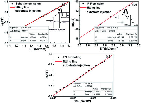
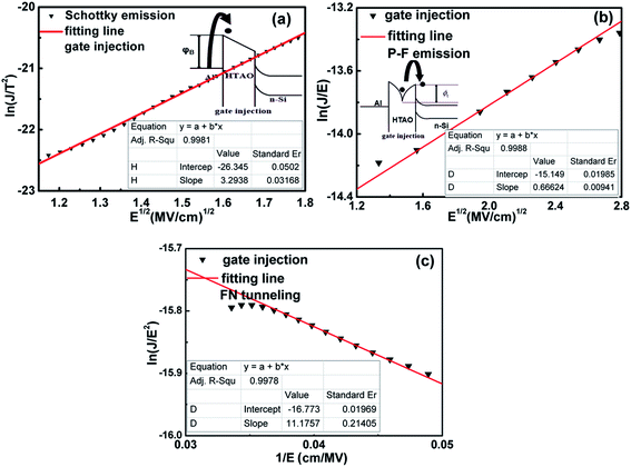
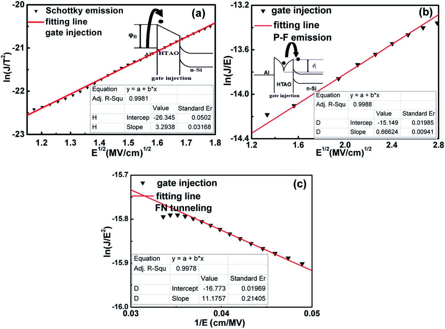
The phenomenon of carrier injection into the gate oxide by tunneling is due to the quantum-mechanical nature of the electron. The MCCT is very complex. For a specific gate dielectric, one or more MCCT plays a major role in a given voltage range. To study the mechanism of carrier charge transport in the Al/HTAO/Si–MOS capacitor, several models for the S4′′ with the best performance were discussed and evaluated in detail for both the gate injection and substrate, including Schottky emission (SE), Poole–Frenkel (PF) emission, and Fowler–Nordheim (FN) tunneling. As shown in Fig. 14 and 15, it is found that the dominating MCCT follows SE emission in the lower electric field, PF emission in the medium electric field, and FN tunneling in the higher electric field.
 |
| | Fig. 14 (a) SE emission, (b) PF emission and (c) FN tunneling plots for S4′′ MOS capacitor under the substrate injection. | |
 |
| | Fig. 15 (a) SE emission, (b) PF emission and (c) FN tunneling plots for S4′′ MOS capacitor under the gate injection. | |
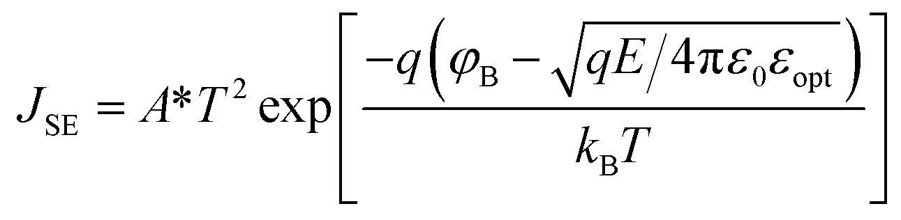
The SE emission model can be described by the equation: 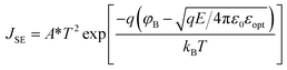 ,34 in which
 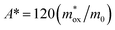 (A cm−2 K−2), T, q, kB, and E denote the Richardson constant, the absolute temperature, the electronic charge, and the Boltzmann constant, respectively. ε0 and εox are the permittivity of vacuum and the relative dielectric constant, respectively. φB represents the potential barrier height between the Al electrode and the conduction band edge Ec of HTAO. As shown in Fig. 14(a) and 15(a), there is a linear relationship between ln(J/T2) and E1/2 (about 6.25–9.61 MV cm−1 and 2.56–6.76 MV cm−1 at substrate injection and gate injection mode), which indicates that the SE emission occurs through the HTAO film. From the extracted equation:
  , the εox and n can be obtained. For the substrate injection and gate injection, the εox is 15.74 and 23.98, respectively. The εox values of gate injection are closer to the values extracted from the CV curve. This result indicates that the SE emission is the dominant current transmission mechanism in the gate injection mode. The corresponding intercept =
  . Combined with the slope of the linear fitting line of FN MCCT, the
  and φB can also be extracted.
The PF emission model follows the equation: 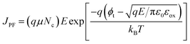 .33 μ and Nc are the mobility of the carrier and the carrier density, respectively. ϕt is the energy barrier from the traps to the conduction band of the dielectric. εox is the dynamic dielectric constant. εox is the square of the refractive index (n). For the PF model, ln(J/E) should have a linear relationship with E1/2. Fig. 14(b) and 15(b) show ln(J/E) vs. E1/2. The plots indicate that there is a linear relation in the middle electric field region (about 6.25–20.24 MV cm−1 and 1.44–7.84 MV cm−1 at the substrate injection and gate injection mode). From the slope of the linear portion:
 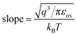 , the εox values extracted are 1942.93 and 5.83 in the substrate injection and gate injection, respectively. The corresponding refractive index n values are 44.08 and 2.42. Compared with n values of Hf-based high-k dielectrics reported in He et al.'s previous work,5,34 the n value for the substrate injection is inconsistent with the experimental value, which indicates that PF emission is the dominant current transmission mechanism. From the intercept of the linear fitting line at the longitudinal coordinate:
 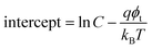 , the ϕt value obtained for substrate injection is 1.90 eV.
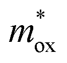
For the FN tunneling model, 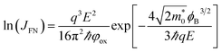 ,33 in which
  is the tunneling effective mass in the HTAO film. Under a high electric field, the carriers will tunnel through the insulator, i.e., electrons are injected into the conduction band of the oxide through the triangular barrier. In the FN model, ln(J/E2) and 1/E would conform to the linear relationship. Fig. 14(c) and 15(c) show ln(J/E2) versus 1/E under substrate injection and gate injection, respectively. It can be seen that the MCCT at a higher electric region appears to follow the FN model in both the substrate and gate injection mode. The slope of the linear portion corresponds to the following expression:
  . In conjunction with the intercept equation of the SE emission,
  and φB can be obtained. Using a self-consistent method, through matching the intercept of the SE model and the slope of the FN model in gate injection mode, the functional relationship between
  and qφB can be expressed as in Fig. 16. The red curve belongs to the FN mode and the blue curve corresponds to the SE mode. It can be seen that the qφB increases as the
  decreases for the SE model, while for the FN model, the qφB increases as the
  increases. The two curves intersect at a point whose value (0.33m0, 1.2 eV) is the required
  and qφB value. It is known that the work function of Al is 4.28 eV,35 the electron affinity potential of Si (χ) is 4.13 eV, and the Ec value of the HTAO film relative to Si is 2.47 eV as obtained above; thus, the energy band structure for the Al/HTAO/Si–MOS capacitor under gate injection is outlined in Fig. 17.
 |
| | Fig. 16 The relationships between  and qφB obtained by fitting the intercept of the SE plots and the slope of the FN plots under the gate injection mode. and qφB obtained by fitting the intercept of the SE plots and the slope of the FN plots under the gate injection mode. | |
 |
| | Fig. 17 The energy band structure for the Al–HTAO–Si–MOS capacitor under the gate injection. | |
4. Conclusion
In this work, the interfacial characteristics, band alignment and electrical performance of ALD-grown HTO, TAO and HTAO gate dielectric films on n-Si wafers were investigated in detail. The experimental results indicate that HfO2 doped with TiO2 can increase the permittivity, but it deteriorates the interface quality and induces increased leakage currents. While incorporating Al2O3 into TiO2 can improve the interface quality and reduce leakage current, it must be at the expense of the dielectric constant. Importantly, the quaternary oxide HTAO synthesized by doping TiO2 and Al2O3 into HfO2 has excellent interface quality and electrical properties. However, an appropriate element ratio is necessary for the HTAO film to possess excellent performance. The interface analysis, band alignment and electrical characterization indicate that the HTAO sample with an ALD cycle ratio of Hf:Ti:Al = 6:1:1 exhibits the most excellent film quality, interface performance and electrical properties.
Conflicts of interest
The authors declare no conflict of interest statement.
Acknowledgements
The authors acknowledge the support from National Natural Science Foundation of China (11774001, 51572002, 51702003), open fund for Discipline Construction, Institute of Physical Science and Information Technology, Anhui University (S01003101), Technology Foundation for Selected Overseas Chinese Scholar, Ministry of Personnel of China (J05015131), Anhui Provincial Natural Science Foundation (1808085ME130), the Provincial Foundation for Excellent Young Talents of Colleges and Universities of Anhui Province (No. gxgwfx2019016), and the Foundation of Co-operative Innovation Research Center for Weak Signal-Detecting Materials and Devices Integration, Anhui University (Y01008411).
References
- Advanced Gate Stacks for High-Mobility Semiconductors, ed. A. Dimoulas, E. Gusev, P. McIntyre and M. Heyns, Springer, Berlin Heidelberg, 2007, pp. 293–310 Search PubMed.
- K. Choi, H. Jagannathan, C. Choi, L. Edge, T. Ando, M. Frank, P. Jamison, M. Wang, E. Cartier, S. Zafar and J. Bruley, 2009 Symposium on VSLI Technology, 2009, pp. 138–139 Search PubMed.
- B.-E. Park, Y. Lee, I.-K. Oh, W. Noh, S. Gatineau and H. Kim, J. Mater. Sci., 2018, 53, 15237–15245 CrossRef CAS.
- H. Zhu, C. Tang and L. R. C. Fonseca, J. Mater. Sci., 2012, 47, 7399–7416 CrossRef CAS.
- G. He, Z. Q. Sun and G. Li, Crit. Rev. Solid State Mater. Sci., 2012, 37, 131–157 CrossRef CAS.
- L. Feng, N. Li and H. Tian, J. Mater. Sci., 2014, 49, 1875–1881 CrossRef CAS.
- J. Gao, G. He, Z. Q. Sun, H. S. Chen, C. Y. Zheng, P. Jin, D. Q. Xiao and M. Liu, J. Alloys Compd., 2016, 667, 352–358 CrossRef CAS.
- C. X. Li, X. Zou, P. T. Lai, J. P. Xu and C. L. Chan, Microelectron. Reliab., 2008, 48, 526–530 CrossRef CAS.
- H. J. Li, J. Price, M. Gardner, N. Lu and D. L. Kwong, Appl. Phys. Lett., 2006, 89, 103523 CrossRef.
- T. Das, C. Mahata, C. K. Maiti, E. Miranda, G. Sutradhar and P. K. Bose, Appl. Phys. Lett., 2011, 98(2), 042120 CrossRef.
- N. Lu, H.-J. Li, J. J. Peterson and D. L. Kwong, Appl. Phys. Lett., 2007, 90, 082911 CrossRef.
- R. L. Puurunen, J. Appl. Phys., 2005, 97, 121301 CrossRef.
- S. M. George, Chem. Rev., 2010, 110, 111–131 CrossRef CAS PubMed.
- N. Pinna and M. Knez, Atomic layer deposition of nanostructured materials, John Wiley & Sons, 2012 Search PubMed.
- C. Ye, H. Wang, J. Zhang, Y. Ye, Y. Wang, B. Y. Wang and Y. C. Jin, J. Appl. Phys., 2010, 107, 104103 CrossRef.
- E. A. Kraut, R. W. Grant, J. R. Waldrop and S. P. Kowalczyk, Phys. Rev. Lett., 1980, 198044, 1620–1622 CrossRef.
- J. W. Zhang, G. He, M. Liu, H. S. Chen, Y. M. Liu, Z. Q. Sun and X. S. Chen, Appl. Surf. Sci., 2015, 346, 489–496 CrossRef CAS.
- L. Fleming, C. C. Fulton and G. Lucovsky, J. Appl. Phys., 2007, 102, 033707 CrossRef.
- G. Lucovsky, C. C. Fulton, Y. Zhang, J. Luning, L. Edge and J. L. Whitten, Thin Solid Films, 2005, 486, 129–135 CrossRef CAS.
- N. Novkovski, Mater. Sci. Semicond. Process., 2015, 39, 308–317 CrossRef CAS.
- R. Engel-Herbert, Y. Hwang and S. Stemmer, J. Appl. Phys., 2010, 108, 124101 CrossRef.
- D. K. Schroder, Semiconductor Material and Device Characterization, John Wiley and Sons, Inc., New York, 1990 Search PubMed.
- S. Guha, E. P. Gusev, H. Okorn-Schmidt, M. Copel, L.-Å. Ragnarsson, N. A. Bojarczuk and P. Ronsheim, Appl. Phys. Lett., 2002, 81, 2956–2958 CrossRef CAS.
- S. Jakschik, U. Schroeder and T. Hecht, Appl. Surf. Sci., 2003, 211, 352–359 CrossRef CAS.
- A. J. Elliot, G. Malek, L. Wille, R. Lu, S. Han and J. Z. Wu, IEEE Trans. Appl. Supercond., 2013, 23, 1101405 Search PubMed.
- J. Gao, G. He, J. W. Zhang, X. F. Chen, P. Jin, D. Q. Xiao, M. Liu, R. Ma and Z. Q. Sun, J. Nanosci. Nanotechnol., 2016, 16, 8075–8082 CrossRef CAS.
- J. Gao, G. He, D. Wang and S. Liang, J. Vac. Sci. Technol., A, 2019, 37, 011101 CrossRef.
- Y. An, C. Mahata, C. Lee, S. Choi, Y.-C. Byun, Y.-S. Kang, T. Lee, J. Kim, M. Cho and H. Kim, J. Phys. D: Appl. Phys., 2015, 48, 415302 CrossRef.
- M. L. Huang, Y. C. Chang, Y. H. Chang, T. D. Lin, J. Kwo and M. Hong, Appl. Phys. Lett., 2009, 94, 052106 CrossRef.
- M. Perego, G. Seguini, G. Scarel, M. Fanciulli and F. Wallrapp, J. Appl. Phys., 2008, 103, 043509 CrossRef.
- A. P. Alekhin, A. A. Chouprik, S. A. Gudkova, A. M. Markeev, Y. Y. Lebedinskii, A. M. Matveyev and A. V. Zenkevich, J. Vac. Sci. Technol., B: Nanotechnol. Microelectron.: Mater., Process., Meas., Phenom., 2011, 29, 01A302 Search PubMed.
- A. P. Alekhin, A. A. Chouprik, I. P. Grigal, S. A. Gudkova, Y. Y. Lebedinskii, A. M. Markeev and S. A. Zaitsev, Thin Solid Films, 2012, 520, 4547–4550 CrossRef CAS.
- R. P. Ortiz, A. Facchetti and T. J. Marks, Chem. Rev., 2010, 110, 205–239 CrossRef CAS PubMed.
- G. He, L. Q. Zhu, M. Liu, Q. Fang and L. D. Zhang, Appl. Surf. Sci., 2007, 253, 3413–3418 CrossRef CAS.
- P. M. Tirmali, A. G. Khairnar, B. N. Joshi and A. M. Mahajan, Solid-State Electron., 2011, 62, 44–47 CrossRef CAS.
|
| This journal is © The Royal Society of Chemistry 2020 |
Click here to see how this site uses Cookies. View our privacy policy here. 
 Open Access Article
 This Open Access Article is licensed under a Creative Commons Attribution-Non Commercial 3.0 Unported Licence
 abd,
Gang He*bc,
Lin Haob,
Die Wangb and
Lin Zhaoa
abd,
Gang He*bc,
Lin Haob,
Die Wangb and
Lin Zhaoa


 ,34 in which
 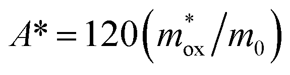 (A cm−2 K−2), T, q, kB, and E denote the Richardson constant, the absolute temperature, the electronic charge, and the Boltzmann constant, respectively. ε0 and εox are the permittivity of vacuum and the relative dielectric constant, respectively. φB represents the potential barrier height between the Al electrode and the conduction band edge Ec of HTAO. As shown in Fig. 14(a) and 15(a), there is a linear relationship between ln(J/T2) and E1/2 (about 6.25–9.61 MV cm−1 and 2.56–6.76 MV cm−1 at substrate injection and gate injection mode), which indicates that the SE emission occurs through the HTAO film. From the extracted equation:
 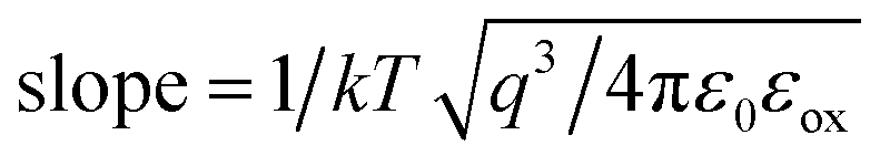 , the εox and n can be obtained. For the substrate injection and gate injection, the εox is 15.74 and 23.98, respectively. The εox values of gate injection are closer to the values extracted from the CV curve. This result indicates that the SE emission is the dominant current transmission mechanism in the gate injection mode. The corresponding intercept =
 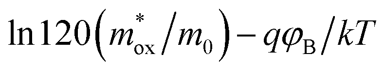 . Combined with the slope of the linear fitting line of FN MCCT, the
  and φB can also be extracted.
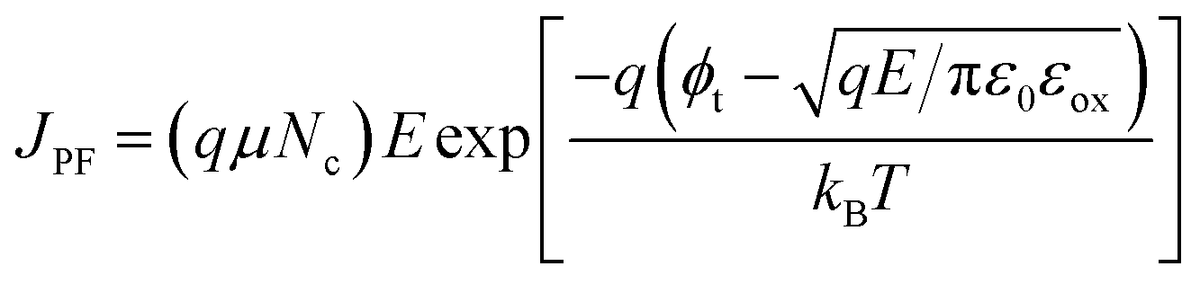 .33 μ and Nc are the mobility of the carrier and the carrier density, respectively. ϕt is the energy barrier from the traps to the conduction band of the dielectric. εox is the dynamic dielectric constant. εox is the square of the refractive index (n). For the PF model, ln(J/E) should have a linear relationship with E1/2. Fig. 14(b) and 15(b) show ln(J/E) vs. E1/2. The plots indicate that there is a linear relation in the middle electric field region (about 6.25–20.24 MV cm−1 and 1.44–7.84 MV cm−1 at the substrate injection and gate injection mode). From the slope of the linear portion:
 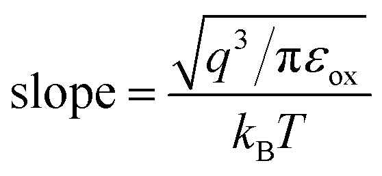 , the εox values extracted are 1942.93 and 5.83 in the substrate injection and gate injection, respectively. The corresponding refractive index n values are 44.08 and 2.42. Compared with n values of Hf-based high-k dielectrics reported in He et al.'s previous work,5,34 the n value for the substrate injection is inconsistent with the experimental value, which indicates that PF emission is the dominant current transmission mechanism. From the intercept of the linear fitting line at the longitudinal coordinate:
  , the ϕt value obtained for substrate injection is 1.90 eV.
 ,33 in which
 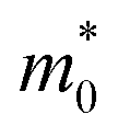 is the tunneling effective mass in the HTAO film. Under a high electric field, the carriers will tunnel through the insulator, i.e., electrons are injected into the conduction band of the oxide through the triangular barrier. In the FN model, ln(J/E2) and 1/E would conform to the linear relationship. Fig. 14(c) and 15(c) show ln(J/E2) versus 1/E under substrate injection and gate injection, respectively. It can be seen that the MCCT at a higher electric region appears to follow the FN model in both the substrate and gate injection mode. The slope of the linear portion corresponds to the following expression:
  . In conjunction with the intercept equation of the SE emission,
 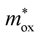 and φB can be obtained. Using a self-consistent method, through matching the intercept of the SE model and the slope of the FN model in gate injection mode, the functional relationship between
  and qφB can be expressed as in Fig. 16. The red curve belongs to the FN mode and the blue curve corresponds to the SE mode. It can be seen that the qφB increases as the
  decreases for the SE model, while for the FN model, the qφB increases as the
  increases. The two curves intersect at a point whose value (0.33m0, 1.2 eV) is the required
  and qφB value. It is known that the work function of Al is 4.28 eV,35 the electron affinity potential of Si (χ) is 4.13 eV, and the Ec value of the HTAO film relative to Si is 2.47 eV as obtained above; thus, the energy band structure for the Al/HTAO/Si–MOS capacitor under gate injection is outlined in Fig. 17.
 and qφB obtained by fitting the intercept of the SE plots and the slope of the FN plots under the gate injection mode.