 Open Access Article
First principles study of Schottky barriers at Ga2O3(100)/metal interfaces
Ran Xuab,
Na Lin *ac,
Zhitai Jia
 a,
Yueyang Liu*b,
Haoyuan Wanga,
Yifei Yua and
Xian Zhao*a
aState Key Lab of Crystal Materials, Shandong University, 250100 Jinan, P. R. China. E-mail: linnakth@gmail.com; xianzhao@sdu.edu.cn
bState Key Laboratory of Superlattices and Microstructures, Institute of Semiconductors, Chinese Academy of Sciences, 100083 Beijing, P. R. China. E-mail: yueyangliu@semi.ac.cn
cDepartment of Chemistry, University of Calgary, T2N 1N4 Calgary, Alberta, Canada
First published on 14th April 2020
Abstract
A low Schottky barrier height (SBH) of metal–semiconductor contact is essential for achieving high performance electronic devices. Based on first principles calculations, we have comprehensively investigated the interfacial properties of β-Ga2O3 (100) with different metals including Mg, Ni, Cu, Pd and Pt. SBHs have been calculated via layered partial density of states (PDOS) and validated by visual wavefunctions. The results surprisingly show that Mg contact possesses the lowest SBH of 0.23 eV, while other SBHs range from 1.06 eV for Ni, 1.17 eV for Pd and 1.27 eV for Cu to 1.39 eV for Pt. This shows that SBHs of β-Ga2O3 are not fully dependent on metal work functions due to a Fermi level pinning effect. The tunneling barrier was also calculated via electrostatic potential with a 72.85% tunneling probability of the Mg/Ga2O3 interface. The present study will provide an insight into characteristics of Ga2O3/metal interfaces and give guidance for metal choice for Ga2O3 electronic devices.
1 Introduction
As a fourth generation wide band gap semiconductor material, gallium oxide (Ga2O3) is getting more and more attention due to its excellent properties and wide potential applications in the fields of power devices and optoelectronic devices.1–3 There exist five crystalline phases, namely α, β, γ, δ, and ε, among which the β-phase is the most stable phase. β-Ga2O3 with a wide band gap (∼4.9 eV) possesses a high critical breakdown field (Ec) of 8 MV cm−1,4,5 resulting in a huge Baliga figure-of-merit (BFOM) of more than 3000 which is far better than other wide band gap semiconductors such as GaN and SiC.6,7 In addition, large-size single-crystal β-Ga2O3 substrates can be synthesized through conventional melt growth methods, including Edge-defined Film-fed Growth (EFG).8,9It is known that the contact properties between metal and semiconductor can greatly impact the performance of electronic devices. Generally, different metals contact with a semiconductor would form an energy barrier at the interface, which is called Schottky barrier (SB) and responsible for current transport.10 A low SBH can induce a low contact resistance which is of great significance for interfacial electron transfer and besides reduce devices' power consumption.11
Relevant experiments of Ga2O3 SB have been conducted in previous studies. Some researchers have observed that SBHs varied with different metal contacts by using IPE measurements,12 ranging from 1.27 eV for Pd, 1.54 eV for Ni, 1.58 eV for Pt and 1.71 eV for Au. It seems that the dependence of the SBH on metal work function is not obvious for metal/β-Ga2O3 (010) interface. In the same year, Yao's group reported Schottky diodes concerning β-Ga2O3 with five metals (W, Cu, Ni, Ir and Pt).13 SBHs were in the range of 1.0–1.3 eV and 1.6–2.0 eV by performing respectively current–voltage (I–V) and capacitance–voltage (C–V) measurements, which showed little dependence on the metal work functions. However, research on the SBH of metal/β-Ga2O3 (100) interface is limited. Nowadays, theoretical calculation based on first principles is allowed to simulate more kinds of metal contacts, which furthermore helps to explore the regularity of SBHs between interfaces under a same condition without being affected by experimental environment. Moreover, to the best of our knowledge, theoretical study of SBHs on Ga2O3/metal interface is very limited, probably due to the complexity of Ga2O3 interfacial configurations or the interference of metal-induced gap states (MIGS). SBH is usually affected by interfacial structures, surface states, defects, work functions and so on.14 It is necessary to obtain accurate SBHs without the interference of MIGS15 and evaluate its properties.
In present paper, we provide a theoretical study of the contacts between β-Ga2O3 (100) and a series of common metals (Mg, Cu, Pd, Ni, Pt) by performing first principles calculations. The hybrid functional method of Heyd, Scuseria and Ernzerhof (HSE06) was used to describe the electronic structure of the contacts which had been proven to show a better agreement with the experimental results than LDA or GGA methods.16,17 To obtain an explicit SBH, we use layer-resolved PDOS to display a clear semiconductor band gap combined with the visual wavefunctions to show the influence of MIGS. Finally, our theoretical results are in good agreement with the experimental observations.
2 Computational methods
In our study, we have chosen the (100) face of β-Ga2O3 in the calculation, which has been proven to be a stable face by previous DFT studies.18 We do have considered the possibility of using other planes, for example, (010) and (![[2 with combining macron]](https://www.rsc.org/images/entities/char_0032_0304.gif) 01). In contrast, the (100) plane is nonpolar18 and shows good convergence. Furthermore, experiment19 showed that the dependence on different planes is not very notable. Therefore, we construct interfaces with ten-layer (100) oriented β-Ga2O3 and four-layer metal atoms. For Ni, Pd, Cu and Pt metals, which are all with face-centered cubic structures, (111) face is the natural growth face and the most commonly used one in the experiment and first principles calculations.20–22 While Mg metal has a hexagonal close packed structure, (0001) face is the most commonly used.23 A vacuum layer of 15 Å is set to ensure decoupling between neighboring slabs. In our models, the lattice constant of Ga2O3 slab was fixed while the lattice constants of metals were adjusted in order to accommodate reliable prediction on the band gap of Ga2O3, which furthermore predicts reliable SBH. The corresponding lattice constant mismatches range from 2.9% to 8.6%, as given in Table 1. A convergence test with respect to the thickness of both the metal and the Ga2O3 has been conducted. During relaxation of the configurations, we allowed the six layers of Ga2O3 atoms near the interface and metal atoms to interact. The dangling bonds on the Ga2O3 surface were passivated by hydrogen atoms (see Fig. 1) to reduce the effect of surface states, which is a very commonly used method to treat semiconducting surfaces in first principles studies.24–26 The pseudopotential hydrogen of 0.33 was used, according to the amount of lacked electron calculated by charge conservation for the dangling bonds of both Ga and O atoms on this Ga2O3 surface. The hydrogen atoms were also relaxed in the optimization process.
01). In contrast, the (100) plane is nonpolar18 and shows good convergence. Furthermore, experiment19 showed that the dependence on different planes is not very notable. Therefore, we construct interfaces with ten-layer (100) oriented β-Ga2O3 and four-layer metal atoms. For Ni, Pd, Cu and Pt metals, which are all with face-centered cubic structures, (111) face is the natural growth face and the most commonly used one in the experiment and first principles calculations.20–22 While Mg metal has a hexagonal close packed structure, (0001) face is the most commonly used.23 A vacuum layer of 15 Å is set to ensure decoupling between neighboring slabs. In our models, the lattice constant of Ga2O3 slab was fixed while the lattice constants of metals were adjusted in order to accommodate reliable prediction on the band gap of Ga2O3, which furthermore predicts reliable SBH. The corresponding lattice constant mismatches range from 2.9% to 8.6%, as given in Table 1. A convergence test with respect to the thickness of both the metal and the Ga2O3 has been conducted. During relaxation of the configurations, we allowed the six layers of Ga2O3 atoms near the interface and metal atoms to interact. The dangling bonds on the Ga2O3 surface were passivated by hydrogen atoms (see Fig. 1) to reduce the effect of surface states, which is a very commonly used method to treat semiconducting surfaces in first principles studies.24–26 The pseudopotential hydrogen of 0.33 was used, according to the amount of lacked electron calculated by charge conservation for the dangling bonds of both Ga and O atoms on this Ga2O3 surface. The hydrogen atoms were also relaxed in the optimization process.
| Metal | WM (eV) | Mismatch (%) | ds-m (Å) | Eb (eV) | Natoms | Φt (eV) | Φe (eV) |
|---|---|---|---|---|---|---|---|
| Mg | 3.81 | 3.0 | 2.10 | 0.47 | 60 | 0.23 (n) | 0.1 (ref. 32) |
| Ni | 4.49 | 8.6 | 2.13 | 0.54 | 98 | 1.06 (n) | 0.97–1.55 (ref. 12, 19 and 13) |
| Pd | 5.83 | 3.2 | 2.28 | 0.40 | 98 | 1.17 (n) | 1.01–1.29 (ref. 12 and 19) |
| Cu | 5.20 | 3.0 | 2.10 | 0.37 | 72 | 1.27 (n) | 1.13–1.36 (ref. 13 and 33) |
| Pt | 5.73 | 2.9 | 2.28 | 0.13 | 98 | 1.39 (n) | 1.05–1.58 (ref. 12 and 13) |
All calculations, including geometry optimization and electronic structure calculation, were performed with the Norm-Conserving Pseudopotential (NCPP) implemented in the plane-wave package PWmat code27,28 which has been proven to be an accurate and efficient package to calculate large semiconducting systems.29 The Perdew–Berk–Ernzerhof (PBE) exchange-correlation functional was used30,31 to optimize the structure with a plane wave energy cutoff of 60 Ryd. The Monkhorst–Pack k-point mesh was set to 3 × 2 × 1 for the model of 98 atoms, and the force threshold was set to 0.02 eV Å−1. The convergence tolerance of energy is 1 × 10⁻⁵ eV. HSE06 hybrid functional was used to calculate the electronic structure with a mixing parameter of 0.34. We yielded a band gap of 4.9 eV for β-Ga2O3 bulk, which shows a good agreement with the experimental value.1
3 Results and discussions
3.1. Geometry and stability of β-Ga2O3/metal interfaces
The optimized configurations of Ga2O3 (100)/metal contacts are shown in Fig. 1. All systems have achieved convergence criteria. The interlayer distances (ds-m), determined by minimizing the total energy, are 2.10 Å, 2.13 Å, 2.28 Å, 2.10 Å and 2.28 Å for Mg/Ga2O3, Ni/Ga2O3, Pd/Ga2O3, Cu/Ga2O3 and Pt/Ga2O3 interfaces, respectively. Mg/Ga2O3 and Cu/Ga2O3 contacts show small interfacial equilibrium distance of 2.10 Å. While Pd/Ga2O3 and Pt/Ga2O3 interfaces reveal an interfacial spacing more than 2.2 Å which indicate a physical combination. In order to evaluate the stability of the contact structure, we calculated the binding energy of the Ga2O3/metal interfaces, as collected in Table 1. The binding energy (Eb) per interface Ga or O atom is defined as:| Eb = (EGa2O3 + EM − EGa2O3−M)/N |
3.2 Electronic properties
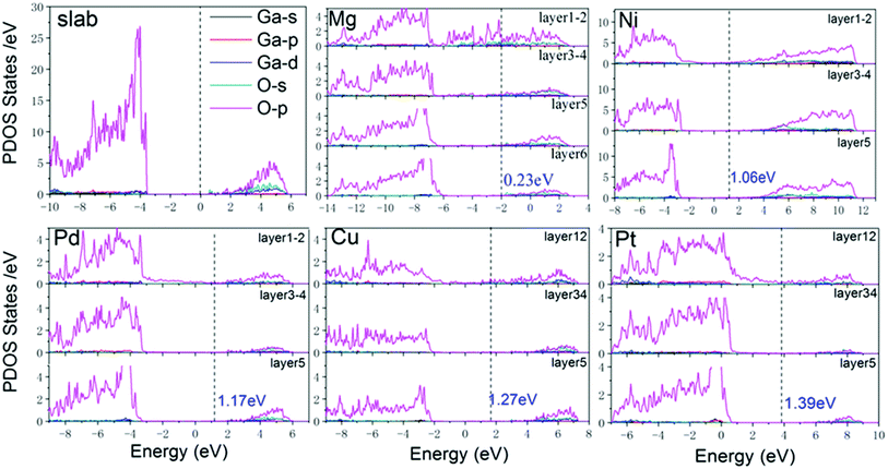
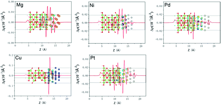
To analyze the electrical properties of Ga2O3/metal contacts, the layer-resolved PDOS are displayed in Fig. 2. The Fermi level is marked by a vertical dashed line, and the Ga2O3 PDOS of layer 1–2, layer 3–4, and layer 5 near the interface are clearly shown in the figure. For comparison, the PDOS of freestanding Ga2O3 is also shown in the first diagram of Fig. 2. It shows a 4.0 eV band gap of Ga2O3 surface smaller than the bulk, which is consistent with previous finding, that generally the band gap of semiconducting slab is reduced relative to the bulk due to the effect of surface states.34 The valence band maximum (VBM) consists of O-p states predominantly together with minor Ga components, whereas the conduction band minimum (CBM) is characterized by a combined contribution of O-s states, Ga-s states and O-p states, which are consistent with previous researches.35,36 For the layer 1–2 of all interfacial systems, PDOS show obvious MIGS with continuous and minute states that exist in the band gap of Ga2O3. MIGS belong to semiconductor intrinsic surface states, which are also called interface states, will decay gradually away from the interface.37–39 In the Fig. 2, we can see that interface states significantly reduce in the 3–4 layers, which furthermore almost disappear in the 5th layer of all contacts. Moreover, the band gap of Ga2O3 is becoming more unambiguous as the interface states fade away. Particularly, Mg interface appears obviously sharp peaks in the band gap of 1–2 layered PDOS due to the interfacial atomic orbital hybridization and strong interaction between the interfaces, which indicate a chemical binding. Therefore, we have shown the layer-6 atomic PDOS of Ga2O3/Mg interface. The magnitude of the SBH depends on the position of the Fermi level at the interface.40 As we can easily see that the five contacts are all n-type SB according to the position of Fermi level. However, it is hard to derive exact SBH from undetermined CBM. Therefore, visual wavefunctions were used to validate the SBHs as follows.In order to further understand the charge transfer and charge distribution between Ga2O3 and metal after interface formation, we explored the charge density difference in the direction perpendicular to the interface. For quantitative analysis, the plane-averaged charge density difference perpendicularly to the interface is also calculated, as shown in Fig. 3 with red curves. The charge density difference is defined as:
| Δρ(z) = ρGa2O3−M(z) − ρGa2O3(z) − ρM(z) |
3.3. Schottky barrier and tunneling barrier at Ga2O3–metal contacts
SB plays a key role in the metal–semiconductor interface research, which can primarily influence the electron transport in device. The SBH can be acquired from the difference between Fermi level of interfacial systems and identifiable CBM/VBM of Ga2O3. The CBM of Ga2O3 derived from the 5th layered PDOS is uncertain, therefore, we furthermore analyzed their wavefunctions to confirm. Wave functions of Ga2O3/Mg and Ga2O3/Cu systems have been used as two examples in Fig. 4, where some representative eigen values were selected to plot visual wavefunctions according to the PDOS of Cu and Mg systems in Fig. 2. | ||
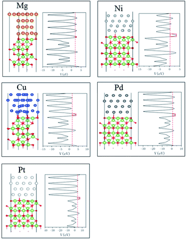
| Fig. 4 Visual wavefunction of Ga2O3/Cu at (a) 2.11 eV (b) 3.01 eV and Ga2O3/Mg at (c) −2.12 eV (d) −1.67 eV. Yellow areas denote wavefunction distribution. | ||
Through the distribution of wavefunctions marked by yellow, it is feasible to recognize the local wavefunction and continuous wavefunction. MIGS are reflected in Fig. 4(a) and (c) in which wavefunctions cover all metal atoms and local Ga2O3 interfacial atoms, with 2.11 eV and −2.12 eV energy eigenvalues corresponding to the energy of semiconducting band gap in the PDOS of Ga2O3/Cu and Ga2O3/Mg, respectively. We had tested different eigenvalues which near the corresponding band edge of Ga2O3, until wavefunctions wrap all Ga2O3 atoms as displayed in Fig. 4(b) and (d). In this way, the CBM values were found similar to the 5th layered PDOS of the two contacts. By this approach, accurate electron SBHs of all contacts have been determined to be respectively 0.23 eV, 1.06 eV, 1.17 eV, 1.27 eV and 1.39 eV for Ga2O3/Mg, Ga2O3/Ni, Ga2O3/Pd, Ga2O3/Cu and Ga2O3/Pt without interference of interface states. Besides, in Fig. 4(c) we can see wavefunctions obviously cover in Ga2O3/Mg interfacial region which indicates a strong interaction between the contacts. While energy reaches −1.67 eV, wavefunctions start distributing on both Ga2O3 and metal atoms which can be interpreted by the coupling effect of the two slabs, as shown in Fig. 4(d).
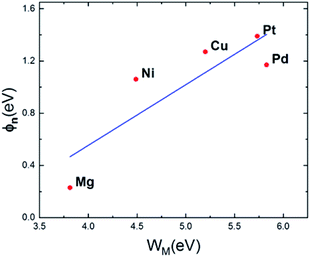
The metal work functions using strain calculated by DFT method41,42 are collected in Table 1. Fig. 5 visualizes the relationship between metal work functions and SBHs. The slope of the blue fit line is approximately 0.40 which shows a little dependence of SBH on metal work functions. It does not conform to Schottky–Mott behavior43 of Ga2O3 semiconductor, since a certain density of interface states can pin the Fermi level inside the semiconducting bandgap. Among them Mg contact possesses the smallest SBH just below the CBM, which derives from both low metal work function and strong interaction between interfaces. However, due to Fermi level pinning,44 SB does not vanish.
The tunneling barrier is another figure to assess the contact performance, which can be calculated by using the average electrostatic potentials of interfacial systems as shown in Fig. 6, in which the Fermi level is marked with red dashed line. The electrostatic potential above Fermi level at the interface is regarded as tunneling barrier which is marked with red rectangle.45 The height and half-width of the rectangle are expressed as the height (ΔV) and width (WB) of tunneling barrier, respectively.46 We can see that among five metals, Mg contact has the least ΔV and notably small WB, indicating higher electron transfer efficiency. It is noted that the coordinate scale in Pd and Pt systems is larger than Mg and Ni systems. They show higher ΔV than other metal contacts in Fig. 6, which indicate low tunneling probabilities. These results were summarized in Table 2. And the tunneling probability (TB) from metals to Ga2O3 can be calculated by the following formula:
 | ||
| Fig. 6 Side view of optimized structures and average electrostatic potential along the direction normal to the metal/Ga2O3 interfaces. | ||
| ΔV (eV) | WB (Å) | TB (%) | |
|---|---|---|---|
| Mg | 0.78 | 0.15 | 72.85 |
| Ni | 2.14 | 0.25 | 41.70 |
| Cu | 2.01 | 0.25 | 42.84 |
| Pd | 2.72 | 0.25 | 37.31 |
| Pt | 2.88 | 0.3 | 29.60 |
4 Conclusion
In summary, we provide the first systematic research on the interfacial SBHs of Ga2O3 with Mg, Ni, Pd, Cu and Pt metals. We draw a conclusion that among the five interfaces Ga2O3/Mg contact possesses the least SBH which indicates an excellent electron transport property. Besides, SBHs of Ga2O3 are not distinctly regulated by metal work functions due to Fermi level pinning. Visual wavefunctions were plotted to give a clear interpretation of the MIGS and confirm the value of SBHs. In the meanwhile, the results provide an insight into the interfacial characteristics of Ga2O3 in contact with metals, which will give useful guidance for the selection of metal in β-Ga2O3 electronic devices.Conflicts of interest
There are no conflicts to declare.Acknowledgements
We acknowledge the National Nature Science Foundation of China (Grant No. 21573129 and 21403300). The authors also acknowledge a generous grant of computer time from the Institute of Semiconductors in Beijing.References
- K. Matsuzaki, H. Hiramatsu, K. Nomura, H. Yanagi, T. Kamiya, M. Hirano and H. Hosono, Thin Solid Films, 2006, 496, 37–41 CrossRef CAS.
- M. Higashiwaki, K. Sasaki, T. Kamimura, M. Hoi Wong, D. Krishnamurthy, A. Kuramata, T. Masui and S. Yamakoshi, Appl. Phys. Lett., 2013, 103, 123511 CrossRef.
- M. H. Wong, K. Sasaki, A. Kuramata, S. Yamakoshi and M. Higashiwaki, IEEE Electron Device Lett., 2016, 37, 212–215 CAS.
- H. H. Tippins, Phys. Rev., 1965, 140, A316–A319 CrossRef.
- M. Orita, H. Ohta, M. Hirano and H. Hosono, Appl. Phys. Lett., 2000, 77, 4166–4168 CrossRef CAS.
- M. Higashiwaki, K. Sasaki, A. Kuramata, T. Masui and S. Yamakoshi, Appl. Phys. Lett., 2012, 100, 13504 CrossRef.
- M. Higashiwaki, K. Sasaki, A. Kuramata, T. Masui and S. Yamakoshi, Phys. Status Solidi A, 2014, 211, 21–26 CrossRef CAS.
- H. Aida, K. Nishiguchi, H. Takeda, N. Aota, K. Sunakawa and Y. Yaguchi, Jpn. J. Appl. Phys., 2008, 47, 8506–8509 CrossRef CAS.
- E. G. Víllora, K. Shimamura, Y. Yoshikawa, K. Aoki and N. Ichinose, J. Cryst. Growth, 2004, 270, 420–426 CrossRef.
- C. Funck and S. Menzel, AIP Adv., 2019, 9, 45116 CrossRef.
- S. Ghosh, R. Raveendran, A. Saeki, S. Seki, M. Namboothiry and A. Ajayaghosh, Acs Appl. Mater. Inter., 2019, 11, 1088–1095 CrossRef CAS PubMed.
- E. Farzana, Z. Zhang, P. K. Paul, A. R. Arehart and S. A. Ringel, Appl. Phys. Lett., 2017, 110, 202102 CrossRef.
- Y. Yao, R. Gangireddy, J. Kim, K. K. Das, R. F. Davis and L. M. Porter, J. Vac. Sci. Technol., B: Nanotechnol. Microelectron.: Mater., Process., Meas., Phenom., 2017, 35, 3D–113D Search PubMed.
- X. Ma, X. Wu, Y. Wang and Y. Dai, Phys. Chem. Chem. Phys., 2017, 19, 18750–18756 RSC.
- M. C. Toroker, D. K. Kanan, N. Alidoust, L. Y. Isseroff, P. Liao and E. A. Carter, Phys. Chem. Chem. Phys., 2011, 13, 16644–16654 RSC.
- A. Alkauskas, P. Broqvist, F. Devynck and A. Pasquarello, Phys. Rev. Lett., 2008, 101, 106802 CrossRef PubMed.
- B. R. Tuttle, Phys. Rev. B: Condens. Matter Mater. Phys., 2004, 70, 125322 CrossRef.
- V. M. Bermudez, Chem. Phys., 2006, 323, 193–203 CrossRef CAS.
- M. E. Ingebrigtsen, L. Vines, G. Alfieri, A. Mihaila, U. Badstübner, B. G. Svensson and A. Kuznetsov, Mater. Sci. Forum, 2017, 897, 755–758 Search PubMed.
- H. Zhong, R. Quhe, Y. Wang, Z. Ni, M. Ye, Z. Song, Y. Pan, J. Yang, L. Yang, M. Lei, J. Shi and J. Lu, Sci. Rep., 2016, 6, 21786 CrossRef CAS PubMed.
- A. Mahmoud, P. Deleuze and C. Dupont, J. Chem. Phys., 2018, 148, 204701 CrossRef PubMed.
- R. Sun, G. Yang, F. Wang, G. Chu, N. Lu and X. Shen, Mater. Sci. Semicond. Process., 2018, 84, 64–70 CrossRef CAS.
- T. Vegge, Phys. Rev. B: Condens. Matter Mater. Phys., 2004, 70, 35412 CrossRef.
- J. A. Steckel, G. Kresse and J. Hafner, Phys. Rev. B: Condens. Matter Mater. Phys., 2002, 66, 155406 CrossRef.
- S. Tanaka, T. Tamura, K. Okazaki, S. Ishibashi and M. Kohyama, Phys. Status Solidi C, 2007, 4, 2972–2976 CrossRef CAS.
- Y. Liu, F. Liu, R. Wang, J. Luo, X. Jiang, R. Huang, S. Li and L. Wang, Phys. Rev. Appl., 2019, 12, 64012 CrossRef CAS.
- W. Jia, Z. Cao, L. Wang, J. Fu, X. Chi, W. Gao and L. Wang, Comput. Phys. Commun., 2013, 184, 9–18 CrossRef CAS.
- W. Jia, J. Fu, Z. Cao, L. Wang, X. Chi, W. Gao and L. Wang, J. Comput. Phys., 2013, 251, 102–115 CrossRef.
- Y. Liu, F. Zheng, X. Jiang, J. Luo, S. Li and L. Wang, Phys. Rev. Appl., 2019, 11, 44058 CrossRef CAS.
- J. Taylor, H. Guo and J. Wang, Phys. Rev. B: Condens. Matter Mater. Phys., 2001, 63, 121104 CrossRef.
- J. P. Perdew, K. Burke and M. Ernzerhof, Phys. Rev. Lett., 1996, 77, 3865–3868 CrossRef CAS PubMed.
- J. Shi, X. Xia, Q. Abbas, J. Liu, H. Zhang, Y. Liu and H. Liang, J. Semicond., 2019, 40, 12805 CrossRef CAS.
- D. Splith, S. Müller, F. Schmidt, H. von Wenckstern, J. J. van Rensburg, W. E. Meyer and M. Grundmann, Phys. Status Solidi A, 2014, 211, 40–47 CrossRef CAS.
- X. Zhou, E. J. M. Hensen, R. A. van Santen and C. Li, Chem. - Eur. J., 2014, 20, 6915–6926 CrossRef CAS PubMed.
- Y. Li, C. Yang, L. Wu and R. Zhang, Mod. Phys. Lett. B, 2017, 31, 1750172 CrossRef CAS.
- K. Yamaguchi, Solid State Commun., 2004, 131, 739–744 CrossRef CAS.
- J. Chen, Z. Zhang, Y. Guo and J. Robertson, Microelectron. Eng., 2019, 216, 111056 CrossRef CAS.
- J. Goniakowski and C. Noguera, Interface Sci., 2004, 12, 93–103 CrossRef CAS.
- M. Farmanbar and G. Brocks, Phys. Rev. B: Condens. Matter Mater. Phys., 2015, 91, 161304 CrossRef.
- N. R. D'Amico, G. Cantele, C. A. Perroni and D. Ninno, J. Phys.: Condens. Matter, 2015, 27, 15006 CrossRef PubMed.
- N. E. Singh-Miller and N. N. Marzari, Phys. Rev. B: Condens. Matter Mater. Phys., 2009, 80, 235407 CrossRef.
- X. Ma, Y. Dai, L. Yu and B. Huang, Nanoscale, 2016, 8, 1352–1359 RSC.
- J. R. Lince, D. J. Carr E and P. D. Fleischauer, Phys. Rev. B: Condens. Matter Mater. Phys., 1987, 36, 1647–1656 CrossRef CAS PubMed.
- C. Gong, L. Colombo, R. M. Wallace and K. Cho, Nano Lett., 2014, 14, 1714 CrossRef CAS PubMed.
- G. Lee, S. Kim, S. Jhi and H. Lee, Nat. Commun., 2015, 6, 6181 CrossRef CAS PubMed.
- Y. Wang, R. X. Yang, R. Quhe, H. Zhong, L. Cong, M. Ye, Z. Ni, Z. Song, J. Yang, J. Shi, J. Li and J. Lu, Nanoscale, 2016, 8, 1179–1191 RSC.
| This journal is © The Royal Society of Chemistry 2020 |


