
 Open Access Article
 This Open Access Article is licensed under a
 Creative Commons Attribution 3.0 Unported Licence
The deposition and wet etching of Mg-doped ZnO films and their applications for solidly mounted resonators
Chengzhang Han ab,
Haoran Maa,
Yanping Wanga,
Jing Liua,
Lihua Tenga,
Hao Lva,
Qiuling Zhao*a and
Xia Wang*a
ab,
Haoran Maa,
Yanping Wanga,
Jing Liua,
Lihua Tenga,
Hao Lva,
Qiuling Zhao*a and
Xia Wang*a
aOptoelectronic Materials and Technologies Engineering Laboratory, Shandong, Physics Department, Qingdao University of Science and Technology, Qingdao 266042, China. E-mail: sdqlzhao@163.com; phwangxia@163.com
bCollege of Mechanical and Electronic Engineering, Qingdao Binhai University, Qingdao, 266555, China
First published on 6th March 2020
Abstract
In this report, a solidly mounted resonator (SMR), consisting of an Au electrode, Mg-doped ZnO (MgXZn1−XO) piezoelectric film and Bragg acoustic reflector, was fabricated on a Si substrate by radio frequency (RF) magnetron sputtering. As a key processing step for the SMR, MgXZn1−XO films with high c-axis orientation were fabricated and the crystalline structure, surface morphology and roughness of the films were investigated. The surface morphology, optical transmittance and shape control of MgXZn1−XO films were investigated by the chemical wet-etching method with various etchants. The profiles and line patterns of MgXZn1−XO films etched with FeCl3·6H2O solutions are satisfactory and fully meet the industrial requirements. The Bragg acoustic reflector, made entirely of metal, has small internal stress and good heat conduction. An SMR based on a MgXZn1−XO piezoelectric film shows a resonant frequency of 2.402 GHz, and the keff2, QS and QP of the SMR are 3.07%, 415 and 546, respectively.
1. Introduction
With the advancement in micro/nano fabrication, film bulk acoustic resonators (FBARs) have been proposed as typical micro-electromechanical system (MEMS) piezoelectrical devices.1–4 As bulk acoustic wave (BAW) devices operating in the GHz range, FBARs have attracted much attention due to their small size, high operating frequency and potential applications in high-frequency communication and mass-sensitive sensor areas.5–8 As a kind of FBAR, solidly mounted resonators (SMRs) are composed of a piezoelectric layer sandwiched between electrodes and Bragg reflector consisting of alternating high and low acoustic impedance quarter-wavelength thick dielectric or metallic layers.9,10 The SMR, with good mechanical strength and excellent acoustic properties, and being closer to CMOS integration, was therefore chosen in this work.11,12In recent decades, owing to excellent piezoelectric property, better quality factor, and high electromechanical coupling coefficient, ZnO is becoming a very promising candidate for FBAR devices as a piezoelectric material.13–16 However, ZnO have the drawback of low longitudinal acoustic wave velocity and low resistance, which limits its application to high sensitivity acoustic sensors.17 MgXZn1−XO, a ternary compound formed by alloying ZnO and MgO, has attracted more and more attention due to its special properties such as higher acoustic velocity and resistance than that of ZnO.18–20 Studies have shown Mg2+ is doped into the ZnO crystal by substituting the Zn2+ position and MgXZn1−XO still maintains the wurtzite crystal structure when the percentage of Mg atoms is less than 33%.21 By controlling the percentage of Mg-doped in the material, the MgXZn1−XO films with satisfactory sound velocity and electromechanical coupling coefficient can be tailored.22
MgXZn1−XO films have been fabricated by a variety of techniques such as magnetron sputtering,23,24 atomic layer deposition,25,26 spray pyrolysis,27,28 pulsed laser deposition (PLD),29,30 and sol–gel coating.31,32 Among these deposition techniques above, magnetron sputtering might be a most practical method because of its high deposition rate, good adhesion and good uniformity, which is suitable for commercialization.33,34 In generally, ZnO thin films can be easily and fast etched by various common etchants such as HCl, HNO3, H2SO4, H3PO4 and so on.35,36 However, anisotropic etching profiles could be generally obtained and the surface shapes are too difficult to control in the acid solutions through a number of experiments, which has a negative impact on etching patterning. Recently, ferric chloride (FeCl3·6H2O) as a kind of representative etchants, has been carried out to solve this problem.37,38
In this paper, we fabricated MgXZn1−XO films with high c-axis orientation by RF magnetron sputtering and characterized structure and surface morphology of MgXZn1−XO films. In addition, we explored the effects of FeCl3·6H2O as a novel etchant on surface morphology, optical transmittance and shape control of MgXZn1−XO films. The novel Bragg acoustic reflector, made entirely of metal, has small internal stress and good heat conduction. We fabricated a SMR based on MgXZn1−XO films and Bragg acoustic reflector with the optimized fabrication condition and investigated the performance of SMR.
2. Experiment
2.1 MgXZn1−XO films deposition
The MgXZn1−XO thin films were deposited on (100) oriented silicon (Si) substrates in the RF magnetron sputtering system with a base pressure of 5 × 10⁻⁵ Pa. MgXZn1−XO (X = 10%) was used as a target source material and a mixture of argon (Ar) (99.999%) and oxygen (O2) (99.999%) was used as sputtering gas. The distance target-to-substrate is about 70 mm and the target diameter is 80 mm.2.2 MgXZn1−XO films wet etching
The sputtered MgXZn1−XO films were standard photolithography processed by a designed pattern mask. About 1 μm thickness positive photoresist (AZ 4620) was coated on the surface of the MgXZn1−XO films by three-step spin coating. After prebaked at 100 °C for 1 min, a mask aligner was used to transfer the pattern design on the mask to the photoresist. After that, the MgXZn1−XO films with patterned photoresist was dipped in the developer solution (AZ 400K) to remove the exposed photoresist, washed and post-baked at 100 °C for 5 min.To acquire patterned MgXZn1−XO films, the wet etching was carried out in dilute HCl, C2H4O2 and FeCl3·6H2O aqueous solution prepared at the concentration values of 0.001 mol l−1, 0.01 mol l−1, and 0.1 mol l−1, respectively. All wet etchings were carried out in an ambient temperature kept at 25 °C and etching time was precisely controlled. After the wet etching process, MgXZn1−XO films were immediately washed by deionized water and dried by nitrogen.
2.3 SMR fabrication
The procedures of the SMR fabrication were be divided into three steps: Bragg reflector deposition, MgXZn1−XO films fabrication, and top electrode deposition. The Bragg reflector, consisting of Ti and W layers, was first deposited on p-type 3 inch Si (100) substrate with 1–10 Ω cm resistivity at 25 °C, and then MgXZn1−XO films were deposited on the top of the Bragg reflector at 300 °C. Lastly, a Au film was deposited on top of MgXZn1−XO films for top electrode. Similar to MgXZn1−XO films, Ti, W, and Au film were also obtained by the RF magnetron sputtering system using Ti, W, and Au targets in a pure Ar atmosphere, respectively. The distance target-to-substrate is about 70 mm and the diameters of all targets are 80 mm. Finally, a thermal annealing process at 300 °C was also performed to relieve the stress in multilayer films to improve the performance of the SMR.2.4 Characterizations
The crystalline structure of MgXZn1−XO films was investigated by X-ray diffraction (XRD, Bruker Advanced D8) using a Cu-Kα radiation (λ = 1.54187 Å) in a θ–2θ scanning mode. The surface morphology and cross-sectional morphology of MgXZn1−XO films were observed by a field emission-scanning electron microscope (FE-SEM, Carl Zeiss Ultra55). The surface roughness (RMS) of MgXZn1−XO films was investigated by atomic force microscopy (AFM, Nanofirst 3000). The optical transmission of MgXZn1−XO films was measured by UV spectrophotometer (PerkinElmer Lambda 750). The cross-sectional morphology of SMR was observed using a FE-SEM. Finally, the frequency response of SMR was measured by S-scattering parameters with a probe station (Cascade EPS 150 RF) and a network analyzer (HP 8712E). All measurements of SMR were carried out in an ambient temperature kept at 25 °C.3. Results and discussions
3.1 MgXZn1−XO films characterization
The sputtering parameters have an important effect on the crystalline structure and crystalline grain size of MgXZn1−XO films, which determine the quality of films. After many experiments and measurements, the optimal sputtering parameters of MgXZn1−XO films with high c-axis orientation and all metal materials in experiments were summarized in Table 1. Fig. 1 shows the XRD patterns of MgXZn1−XO films grown on silicon substrates. For the MgXZn1−XO films, a very strong diffraction peak was observed at 34.4° with a full width at half-maximum (FWHM) of 0.30°, which corresponds to the diffraction from the MgXZn1−XO (002) plane. This indicates that the preferential MgXZn1−XO growth orientation is along the wurtzite c-axis and perpendicular to the surface of substrate.| Sputtering parameters | Ti | W | MgXZn1−XO | Au |
|---|---|---|---|---|
| RF power (W) | 150 | 150 | 250 | 150 |
| Ar flow rate (sccm) | 20 | 20 | 40 | 20 |
| Sputtering pressure (Pa) | 1.5 | 1.5 | 2.5 | 1.5 |
| Substrate temperature (°C) | 300 | 300 | 300 | 300 |
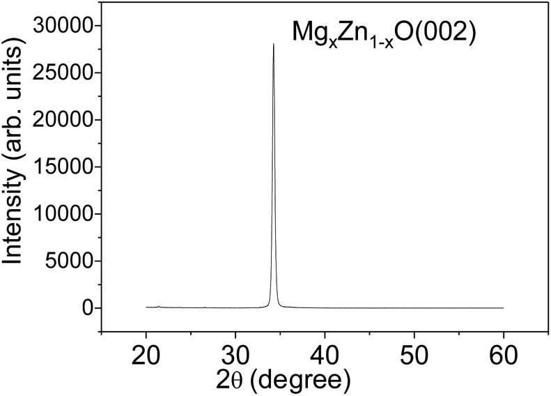 | ||
| Fig. 1 The XRD patterns of MgXZn1−XO films grown on silicon substrates. | ||
Fig. 2 shows the SEM surface and cross-sectional images of MgXZn1−XO films deposited on silicon substrate. The MgXZn1−XO films demonstrate clearly a hummock-like surface morphology with smooth, homogeneous, uncracked, compact and dense. The surface morphology consists of a large number of hexagonal crystalline grains with no visible pores and defects over the films in Fig. 2(a). The MgXZn1−XO films perpendicular to the surface of silicon substrate exhibit highly oriented and compact columnar structure. Besides, the grain boundaries among columns in films and the good cohesion between the MgXZn1−XO films and silicon substrate are observed in Fig. 2(b), obviously.
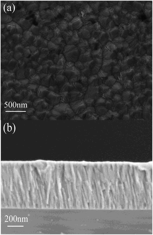 | ||
| Fig. 2 The SEM micrographs obtained for MgXZn1−XO films. (a) Surface image, (b) cross-sectional image. | ||
Fig. 3 shows a three-dimensional AFM image of the MgXZn1−XO films deposited on silicon substrate. The surface roughness of the MgXZn1−XO films is 3.37 nm. The rounded and homogeneous grain shape can be observed from the picture, which reveals the fact that MgXZn1−XO films with a homogeneous smooth surface over the whole wafer. Low surface roughness is connected with low acoustic loss in MgXZn1−XO films, which is suitable for SMR.
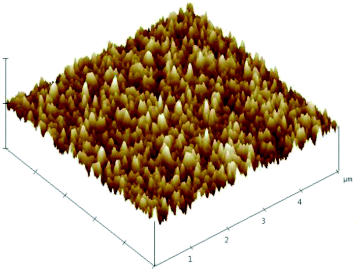 | ||
| Fig. 3 Three-dimensional AFM image of MgXZn1−XO. films deposited on a silicon substrate. | ||
3.2 MgXZn1−XO films etching characteristics
The functions of etching rates and concentrations of different etchant aqueous solutions were shown in Fig. 4. It should be noticed that the etching rate of HCl is most efficient, the C2H4O2 is least, and the FeCl3·6H2O is in between. Under a wide range of etchant concentration, the etching rate almost linearly increases with etchant concentration. It is well known that the etching process of MgXZn1−XO in acid solution is the H+ ions attacking the oxygen atom site on the MgXZn1−XO structure, producing water and soluble salt.39 The higher concentration of H+ ions, the faster etching rate of MgXZn1−XO films. As a kind of strong electrolytes, HCl can be totally ionized to generate enough H+ ions and the concentration of H+ ions is the same as HCl in the aqueous solution, so the etching rate is the fastest. While in FeCl3·6H2O aqueous solution, Fe3+ can react with the H2O by hydrolysis and generate H+ ions. The hydrolysis of Fe3+ can be divided into three steps and H+ ions can be generated in every step, which provides much H+ ions to react with MgXZn1−XO films. Due to the hydrolysis is reversible, Fe3+ can not totally react with the H2O to generate H+ ions, so the concentration of H+ ions in FeCl3·6H2O solutions is lower than HCl solution. This is the reason why the etching rate of FeCl3·6H2O is lower than HCl. It is well known that the C2H4O2 is a kind of weak electrolytes, so only a part of C2H4O2 can be ionized to generate less H+ ions compared to HCl at the same mole concentration. As a result, the concentration of H+ ions is the lowest among the three solutions and the etching rate is lowest. | ||
| Fig. 4 The functions of etching rates and concentrations of different etchant aqueous solutions. | ||
The SEM micrographs of surface texture MgXZn1−XO films etched in different etchants were illustrated in Fig. 5. The concentration of all etchants was controlled to be 0.01 mol l−1 and the etching time was controlled in 1 min. It is observed clearly that the etched samples show distinctive rough surface morphologies due to different etching rates of different etchants. The sample as-grown MgXZn1−XO films without etched consists of close-packed hummock-like crystals surface morphology with smooth, homogeneous and uncracked. By compared, hummock-like crystals are becoming gradually disappeared and the surfaces are becoming gradually rough and cracked with the increase of etching rate in different etchant solutions. It can be proved that surface texture of MgXZn1−XO films is the most severely damaged in HCl solution, the least damaged in C2H4O2 solution, and the moderate in FeCl3·6H2O solution.
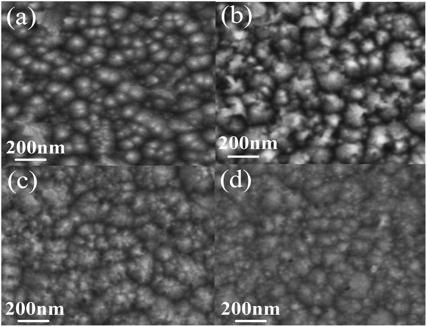 | ||
| Fig. 5 The SEM micrographs of surface texture MgXZn1−XO films etched in different etchants. (a) As-grown, (b) C2H4O2 solution, (c) FeCl3·6H2O solution, (d) HCl solution. | ||
Fig. 6 shows the optical transmittance of MgXZn1−XO films etched in different etchants. The thicknesses of MgXZn1−XO films deposited on glass were 1 μm and the etching time was controlled in 20 s. It was observed clearly that the optical transmittance decrease with the etching rates increase. The etchants destroy the surface morphologies of MgXZn1−XO films and lead to the changes of optical transmittance. The etching rates are faster, the morphologies of destruction are more serious, and the optical transmittances are lower. The results above show that the optical properties can be controlled by varying either etchants or etchants concentration.
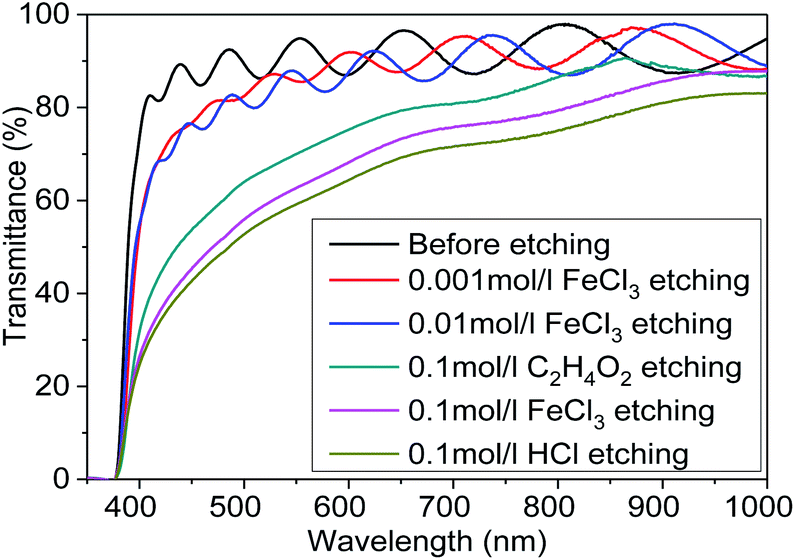 | ||
| Fig. 6 The optical transmittance of MgXZn1−XO films etched in different etchants. | ||
Fig. 7 shows etched profiles of MgXZn1−XO films by different etchants at the same time. The concentration of etchants was controlled to be 0.01 mol l−1 and the etching time was controlled in 3 min. A rough and high in the middle and low on both sides etching profile is observed at the bottom of the step from Fig. 8(a), which results from the faster etching rate near the mask edge than that in the center in HCl solutions. Such kind of etching profile has an adverse effect on the shape and size of the devices and deteriorate devices performance. In contrast, a very smooth etching profile is observed clearly from Fig. 8(b), which results from the same etching rate near both the edge and center of the mask in FeCl3·6H2O solutions. The smooth etching profile in the etched area indicates that the etching rate is almost homogeneous over the entire sample.
 | ||
| Fig. 7 The comparison of etched profiles of the films. (a) Etched in HCl solutions. (b) Etched in FeCl3·6H2O solutions. | ||
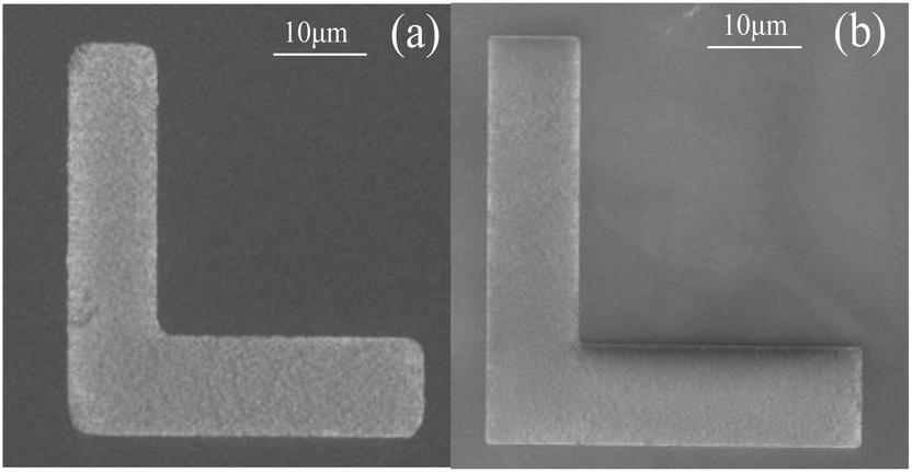 | ||
| Fig. 8 The comparison of right angle line pattern of the MgXZn1−XO films. (a) Etched in HCl solutions. (b) Etched in FeCl3·6H2O solutions. | ||
In addition, Fig. 8 displays the etched right angle line patterns of MgXZn1−XO films in HCl and FeCl3·6H2O solutions. The right angle line patterns etched in HCl solutions displayed a smooth surface and sharp etching step without etching residue in the etched region in Fig. 8(a). But the right angles of the line patterns were destroyed seriously, which indicates that the etching rates along the different directions are not homogeneous on the sample surface. As shown in Fig. 8(b), the problem was settled satisfactorily by FeCl3·6H2O solutions. The right angles of the line patterns etched in FeCl3·6H2O solutions are pointed and integrated, which indicates the etching rates along the different directions are homogeneous on the sample surface and fully meets the requirement of shape and size of the devices.
3.3 SMR characterization
Fig. 9(a) shows a 3D-view schematic illustration of SMR and Fig. 9(b) shows the cross-section view morphologies of integrated SMR with Au/MgXZn1−XO/Ti/W multilayer films structure. The MgXZn1−XO films perpendicular to Bragg reflector exhibit highly oriented and compact columnar structure. The interfaces between the MgXZn1−XO films and Bragg reflector are clearly visible and distinct, verifying that the different membrane layers are not diffusive with each other. As the Bragg reflector was made entirely of metal, it had small internal stress and good heat conduction. Note that top W layer of the Bragg reflector on the top of Si also served as the electrode for frequency measurements.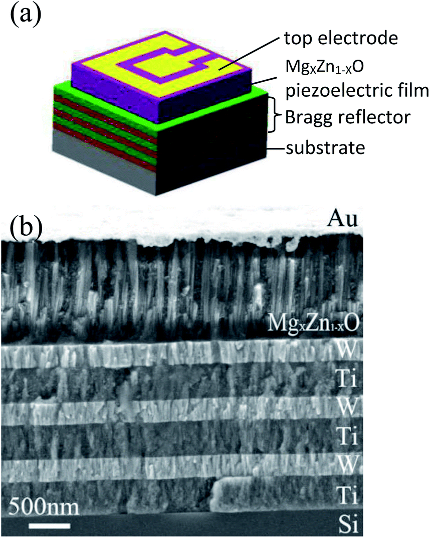 | ||
| Fig. 9 (a) The schematic illustration of SMR. (b) The cross-section view morphologies of integrated SMR. | ||
The reflection coefficient S (1,1), impedance and phase response of SMR were measured with probe station and network analyzer and displayed in Fig. 10. The frequency response of SMR based on MgXZn1−XO films we fabricated is approximately around 2.402 GHz with a return loss of −24.57 dB, and the series resonant frequency (fs) and parallel resonant frequency (fp) appeared at 2.383 GHz and 2.414 GHz, respectively. Both the corresponding coupling coefficient keff2 and quality factor Q values of SMR can be derived easily based upon the formula as follows:40
 | (1) |
 | (2) |
 | ||
| Fig. 10 The reflection coefficient S (1,1), impedance and phase response of SMR. | ||
4. Conclusions
In this paper, we fabricated MgXZn1−XO films with high c-axis orientation by RF magnetron sputtering and investigated the crystalline structure, surface morphology and roughness of films. The effects of different etchants on surface morphology, optical transmittance and shape control of MgXZn1−XO films were very obvious. The FeCl3·6H2O shows better etched profiles and right angle line patterns than other etchants and more suitable for the patterning MgXZn1−XO films. The SMR consisting of MgXZn1−XO films and Bragg acoustic reflector with a resonant frequency of 2.402 GHz, and the keff2, QS and QP of SMR are 3.07%, 415, and 546, respectively. So SMR based on MgXZn1−XO piezoelectric films provides a new approach in the high-frequency communication and sensitive-mass sensor areas.Conflicts of interest
There are no conflicts to declare.Acknowledgements
This work is supported by the Key Research and Development Program of Shandong Province (2018GGX101008) and National Natural Science Foundation of China (11874232).Notes and references
- Q. Yang, S. Pan, Y. Zhao, H. Zhang, W. Pang and X. Duan, Biosens. Bioelectron., 2017, 96, 206–212 CrossRef CAS PubMed.
- X. Zhao, F. Pan, G. M. Ashley, L. Garcia-Gancedo, J. Luo and A. J. Flewitt, et al., Sens. Actuators, B, 2014, 190(1), 946–953 CrossRef CAS.
- D. D. Erbahar, I. Gurol, G. Gümüş, E. Musluoğlu, Z. Z. Öztürk, V. Ahsen and M. Harbeck, Sens. Actuators, B, 2012, 173, 562–568 CrossRef CAS.
- C. Cheng, Y. Chang and Y. Chu, Chem. Soc. Rev., 2012, 41(5), 1947–1971 RSC.
- G. S. Gill and M. Prasad, Sens. Lett., 2016, 14(4), 346–361 CrossRef.
- M. L. Johnston, I. Kymissis and K. L. Shepard, IEEE Sens. J., 2010, 10(6), 1042–1047 CAS.
- C. Han, X. Wang, Q. Zhao, L. Teng, S. Zhang and H. Lv, et al., RSC Adv., 2019, 9, 21323–21328 RSC.
- H. Guo, Y. Gao and T. Liu, Measurement, 2018, 129, 206–210 CrossRef.
- C. Wei, Y. Chen, S. Li, C. Cheng, K. Kao and C. Chung, Appl. Phys. A, 2010, 99(1), 271–278 CrossRef CAS.
- M. Knapp, R. Hoffmann, V. Lebedev, V. Cimalla and O. Ambacher, Nanotechnology, 2018, 29(10), 1–10 CrossRef PubMed.
- Y. Satoh, T. Nishihara, T. Yokoyama, M. Ueda and T. Miyashita, Jpn. J. Appl. Phys., 2005, 44(5A), 2883–2894 CrossRef CAS.
- G. Rughoobur, H. Sugime, M. Demiguel-Ramos, T. Mirea, S. Zheng and J. Robertson, et al., Sens. Actuators, B, 2018, 261, 398–407 CrossRef CAS.
- L. Fan, S. Zhang, H. Ge and H. Zhang, J. Appl. Phys., 2013, 114(2), 0245 CrossRef.
- P. Guo, J. Xiong, D. Zheng, W. Zhang, L. Liu, S. Wang and H. Gu, RSC Adv., 2015, 5(81), 66355–66359 RSC.
- X. He, L. Garcia-Gancedo, P. Jin, J. Zhou, W. Wang and S. Dong, et al., J. Micromech. Microeng., 2012, 22(22), 1519–1529 Search PubMed.
- L. M. Clement, A. Delicado, R. J. Olivares, T. Mirea, J. Sangrador and E. Iborra, Sens. Actuators, A, 2017, 258, 39–43 CrossRef.
- Q. X. Su, P. Kirby, E. Komuro, M. Imura, Q. Zhang and R. Whatmore, IEEE Trans. Microwave Theory Tech., 2001, 49(4), 769–778 CrossRef CAS.
- S. Choopun, R. D. Vispute, W. Yang, R. P. Sharma, T. Venkatesan and H. Shen, Appl. Phys. Lett., 2015, 80(9), 1529–1533 CrossRef.
- N. Chen, H. Wu and D. Qiu, Acta Phys. Sin., 2004, 53(1), 311–315 CAS.
- R. Ghosh and D. Basak, Appl. Surf. Sci., 2009, 255(16), 7238–7242 CrossRef CAS.
- A. Ohtomo, M. Kawasaki, T. Koida, K. Masubuchi, H. Koinuma and Y. Sakurai, et al., Appl. Phys. Lett., 1998, 72(19), 2466–2468 CrossRef CAS.
- N. W. Emanetoglu, S. Muthukumar, P. Wu, R. Wittstruck, Y. Chen and Y. Lu, IEEE Trans. Ultrason. Ferroelectr. Freq. Control, 2003, 50(5), 537–543 Search PubMed.
- T. Minemoto, T. Negami, S. Nishiwaki, H. Takakura and Y. Hamakawa, Thin Solid Films, 2000, 372(2), 173–176 CrossRef CAS.
- H. Chen, J. Ding and S. Ma, Phys. E, 2010, 42(5), 1487–1491 CrossRef CAS.
- T. Törndahl, C. Platzer-Björkman, J. Kessler and M. Edoff, Prog. Photovoltaics, 2007, 15(3), 225–235 Search PubMed.
- J. S. Wrench, I. F. Brunell, P. R. Chalker, J. D. Jin, A. Shaw, I. Z. Mitrovic and S. Hall, Appl. Phys. Lett., 2014, 105(20), 202109 CrossRef.
- P. Prathap P, A. S. Reddy, G. R. Reddy, R. W. Miles and K. T. R. Reddy, Sol. Energy Mater. Sol. Cells, 2010, 94(9), 1434–1436 CrossRef.
- H. Zhang, T. Zhao, G. Hu, L. Miao and Y. Yang, J. Mater. Sci. Lett., 2012, 23(11), 1933–1937 CAS.
- M. Snure and A. Tiwari, J. Appl. Phys., 2007, 101, 124912 CrossRef.
- X. Wang, Z. Chen, C. Hu, K. Saito, T. Tanaka, M. Nishio and Q. Guo, J. Cryst. Growth, 2018, 483, 39–43 CrossRef CAS.
- C. Abed, C. Bouzidi, H. Elhouichet, B. Gelloz and M. Ferid, Appl. Surf. Sci., 2015, 349(2), 855–863 CrossRef CAS.
- D. Zhao, Y. Liu, D. Shen, Y. Lu and J. Zhang, J. Appl. Phys., 2001, 90(11), 5561–5563 CrossRef CAS.
- I. Y. Kim, S. W. Shin, M. G. Gang, S. H. Lee, K. V. Gurav and P. S. Patil, et al., Thin Solid Films, 2014, 570(1), 321–325 CrossRef CAS.
- Z. Lu, L. Long, Z. Zhong and C. Lan, J. Mater. Sci., 2016, 27(3), 2875–2884 CAS.
- S. C. Han, J. K. Kim, J. Y. Kim, K. K. Kim, H. Tampo, S. Niki and J. M. Lee, J. Electrochem. Soc., 2010, 157(1), 60–64 CrossRef.
- W. L. Lu, K. C. Huang, C. H. Yeh, C. I. Hung and M. P. Houng, Mater. Chem. Phys., 2011, 127(1–2), 358–363 CrossRef CAS.
- D. G. Yoo, S. H. Nam, M. H. Kim, S. H. Jeong, H. G. Jee and H. J. Lee, et al., Surf. Coat. Technol., 2008, 202(22–23), 5476–5479 CrossRef CAS.
- H. Zheng, X. L. Du, Q. Luo, J. F. Jia, C. Z. Gu and Q. K. Xue, Thin Solid Films, 2007, 515(7), 3967–3970 CrossRef CAS.
- H. Maki, T. Ikoma, I. Sakaguchi, N. Ohashi, H. Haneda, J. Tanaka and N. Ichinose, Thin Solid Films, 2002, 411(1), 91–94 CrossRef CAS.
- Q. Su, R. Kirby, E. Komuro, M. Imura, Q. Zhang and R. Whatmore, IEEE Trans. Microwave Theory Tech., 2001, 49(4), 769–778 CrossRef CAS.
| This journal is © The Royal Society of Chemistry 2020 |