
 Open Access Article
 This Open Access Article is licensed under a Creative Commons Attribution-Non Commercial 3.0 Unported Licence
Spin relaxation induced by interfacial effects in n-GaN/MgO/Co spin injectors
Xingchen Liu a,
Ning Tang*ad,
Chi Fangb,
Caihua Wan*b,
Shixiong Zhanga,
Xiaoyue Zhanga,
Hongming Guana,
Yunfan Zhanga,
Xuan Qiance,
Yang Jice,
Weikun Gea,
Xiufeng Hanb and
Bo Shenad
a,
Ning Tang*ad,
Chi Fangb,
Caihua Wan*b,
Shixiong Zhanga,
Xiaoyue Zhanga,
Hongming Guana,
Yunfan Zhanga,
Xuan Qiance,
Yang Jice,
Weikun Gea,
Xiufeng Hanb and
Bo Shenad
aState Key Laboratory of Artificial Microstructure and Mesoscopic Physics, School of Physics, Peking University, Beijing 100871, China. E-mail: ntang@pku.edu.cn
bBeijing National Laboratory for Condensed Matter Physics, Institute of Physics, University of Chinese Academy of Sciences, Chinese Academy of Sciences, Beijing 100190, China. E-mail: wancaihua@iphy.ac.cn
cState Key Laboratory for Superlattices and Microstructures, Institute of Semiconductors, Chinese Academy of Sciences, Beijing 100083, China
dFrontiers Science Center for Nano-optoelectronics & Collaboration Innovation Center of Quantum Matter, Peking University, Beijing 100871, China
eCollege of Materials Science and Opto-Electronic Technology, College of Physical Sciences, University of Chinese Academy of Sciences, Beijing 100049, China
First published on 27th March 2020
Abstract
Spin relaxation, affected by interfacial effects, is a critical process for electrical spin injection and transport in semiconductor-based spintronics. In this work, the electrical spin injection into n-GaN via n-GaN/MgO/Co tunnel barrier was realized, and the interface-related spin relaxation was investigated by both electrical Hanle effect measurement and time-resolved Kerr rotation (TRKR) spectrum. It was found that the spin relaxation caused by interfacial random magnetostatic field was nearly equal to the intrinsic contributions at low temperature (less than 80 K) and could be suppressed by smoother n-GaN/Co interface. When the interfacial random magnetostatic field was suppressed, the spin relaxation time extracted from the electrical injection process was still shorter than that in bulk conduction band, which was attributed to Rashba spin–orbit coupling (SOC) induced by the interface band bending in the depletion region. Due to thermal activation, luckily, the spin relaxation induced by the interfacial Rashba SOC was suppressed at temperatures higher than 50 K. These results illustrate that (1) spin relaxation time could be as long as 300 ps for GaN and (2) the influences of interfacial effects could be engineered to further prolong spin relaxation time, both of which shed lights on GaN-based spintronic devices with direct and wide bandgap.
1. Introduction
Spin injection into semiconductors is one of the key elements in developing spintronic devices, such as spin-polarized diode laser,1 circular-polarized light-emitting diodes,2 and spin field-effect transistors (FET).3–5 Owing to relatively weak intrinsic spin–orbit coupling (SOC) in bulk GaN and as-induced long coherent length, bulk GaN and its low-dimensional structures are suitable for long spin transport and effective spin manipulation.6,7 Spin-tunnelling barriers, such as MgO and Al2O3 (ref. 8–12) or Schottky barriers,13–15 are wildly used to overcome the conductance mismatch and increase the spin injection efficiency. However, the localized interfacial states inside the tunnelling barriers may trap spin-polarized electrons13,16,17 and block spin transport into bulk region. Furthermore, the interfacial effects, including localized interfacial states, interfacial random magnetostatic field induced by roughness,18 and the Rashba SOC field induced by the interface band bending,19,20 significantly affect the spin relaxation process, whereas this topic has rarely been investigated systematically,13,16 especially for wide-bandgap semiconductors.Considering the spin relaxation time τs is a critical parameter for spintronic devices, the spin relaxation processes induced by interfacial effects in the n-GaN/MgO/Co spin injectors were studied in this work. By comparing the τs extracted under various temperatures and external magnetic field, different interface-related spin relaxation mechanisms during the spin injection process were identified. In addition, τs extracted from the electrical spin injection process and dominated by interfacial effects is generally different from its bulk counterpart determined by optical method,21 and their differences can reflect the influences of the interfacial effects. Therefore, besides the electrical Hanle effect measurements, here the time-resolved Kerr rotation (TRKR) spectrum was also adopted to measure the τs of the conduction band electrons in the same bulk n-GaN.
2. Experiment
To investigate the spin relaxation processes induced by interfacial random magnetostatic field and interfacial band bending, two types of n-GaN/MgO/Co spin injectors were respectively fabricated in our experiments. The GaN layers of sample A (n-GaN, Si-doped: 1 × 1019 cm−3) and sample B (n-GaN, Si-doped: 1 × 1017 cm−3) were both grown by metal–organic chemical vapor deposition (MOCVD). Their stack structures consisted of 2 μm undoped GaN and 2.5 μm n-GaN grown on a c-axis sapphire substrate, as shown in Fig. 1(a). Then the samples were transferred into an ultrahigh vacuum magneto-sputtering system (ULVAC), where the tunnelling layer (2 nm MgO) and ferromagnetic film (20 nm Co) were deposited, followed by the deposition of 10 nm Pt to avoid oxidation. Finally, the three-terminal devices were fabricated by the standard UV photolithography and ion beam etching. Owing to the higher doping level, the n-GaN surface of sample A was rougher as indicated by atomic force microscopes images (20 μm × 20 μm) which showed the root-mean-square roughness (RMS) of n-GaN was 2.80 nm and 1.25 nm for sample A and B, respectively. The rougher n-GaN/MgO interface caused by the rougher surface of n-GaN made the effect of the interfacial random magnetostatic field in sample A obvious as shown below. Instead, the wider depletion region in sample B caused by the lower doping level guaranteed the remarkable spin relaxation induced by interface band bending.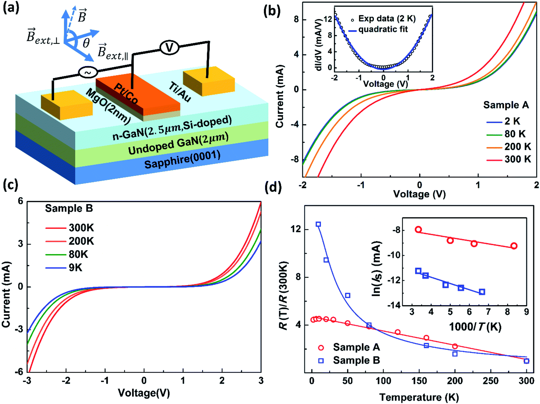 | ||
| Fig. 1 (a) The schematic of the sample structures and setup of three-terminal Hanle effect measurements. (b) The I–V characteristics of the injection circuit of sample A at various temperatures. The inset shows the differential conductance as a function of bias voltages. (c) The I–V characteristics of the injection circuit of sample B at various temperatures. (d) Normalized zero-bias resistance as a function of temperature. The temperature dependence of saturation current is shown in the inset. | ||
The low-temperature magnetotransport measurements were performed within a Physical Properties Measurement System (PPMS-9T, Quantum design). Keithley 2400, Keithley 6221 and a lock-in amplifier were used to conduct the I–V and Hanle effect measurements. The same bulk GaN wafers without spin injectors (MgO/Co/Pt) was used for the TRKR measurements. The pump and probe beams were derived from the frequency-double output of a mode-locked Ti:Sapphire laser, and the beam energy varied from 3.493 eV to 3.444 eV to match the bandgap shift from 9 K to 200 K. The power ratio between the pump and probe beams approached to 10![[thin space (1/6-em)]](https://www.rsc.org/images/entities/char_2009.gif) :1, and the estimated density of photoexcited carriers was 7.57 × 1014 cm−3 at 9 K and 9.25 × 1014 cm−3 at 200 K, respectively. An external magnetic field was provided in the sample plane during the TRKR measurements.
:1, and the estimated density of photoexcited carriers was 7.57 × 1014 cm−3 at 9 K and 9.25 × 1014 cm−3 at 200 K, respectively. An external magnetic field was provided in the sample plane during the TRKR measurements.
3. Results and discussion
The I–V measurements were conducted in the injection circuit by using two terminal geometry. The I–V curves of sample A and sample B at various temperatures (T) are shown in Fig. 1(b) and (c), both of which show a nonlinear and symmetric behaviour with varying the applied bias voltage. The differential conductance, which is deduced by taking the differential of I–V curves with respect to voltage, exhibits a quadratic dependence on the bias voltage. Furthermore, the zero bias resistance (R(T)) is derived by taking the reciprocal of conductance at zero voltage, which is usually used to analyze the tunnelling process.6,22 The T-dependence of the normalized R(T) is shown in Fig. 1(d). For sample A, the R(T) shows a weak dependence on T, which evidences the direct tunnelling (phonon-irrelevant) dominated process.6,22 In contrast, the R(T) of sample B shows a sharp and nonlinear T-dependence, indicating the sequential tunnelling through the localized interfacial states.23,24 To further compare the tunnelling process, the tunnelling barriers of both samples are extracted. The I–V curves at positive bias satisfy I = Isexp(eV/ηkBT) as eV ≫ kBT where Is, η and T are saturation current, ideal factor, and temperature, respectively. The saturation current can be expressed as Is = AT2exp(−Eb/kBT) where Eb is the tunneling barrier.13,25 It turns out that AT2 could be regarded as T-insensitive near room temperature13 compared with the exponential term. Under this approximation, ln(Is) has a linear dependence on 1/T. As shown in the inset of Fig. 1(d), by linearly fitting the dependence of ln(Is) on 1/T, the tunneling barriers are derived as 22 meV and 43 meV for sample A and B, respectively. The higher tunnelling barrier of sample B can result from much lower doping level and indicates the stronger interfacial band bending.
Spin accumulation resulting from electrical spin injection was detected by a three-terminal geometry. The imbalanced spin polarization produces an additional electrochemical potential ΔVs (spin voltage). An external magnetic field (out-of-plane) perpendicular to the spin accumulation (Fig. 1(a)) can reduce ΔVs by Larmor precession, which is so-called the Hanle effect.18,26 The dependence of ΔVs on the perpendicular magnetic field ![[B with combining right harpoon above (vector)]](https://www.rsc.org/images/entities/i_char_0042_20d1.gif) ext,⊥ can be expressed as26
ext,⊥ can be expressed as26
| ΔVs(B) = ΔVs(0)/[1+(ωτs)2] | (1) |
Then the variation of ΔVs under ext,⊥ was detected by a lock-in amplifier. The typical Hanle effect curves of sample A and sample B are shown in Fig. 2(a) and 4(a), respectively, and τs can be extracted from the Hanle curves.
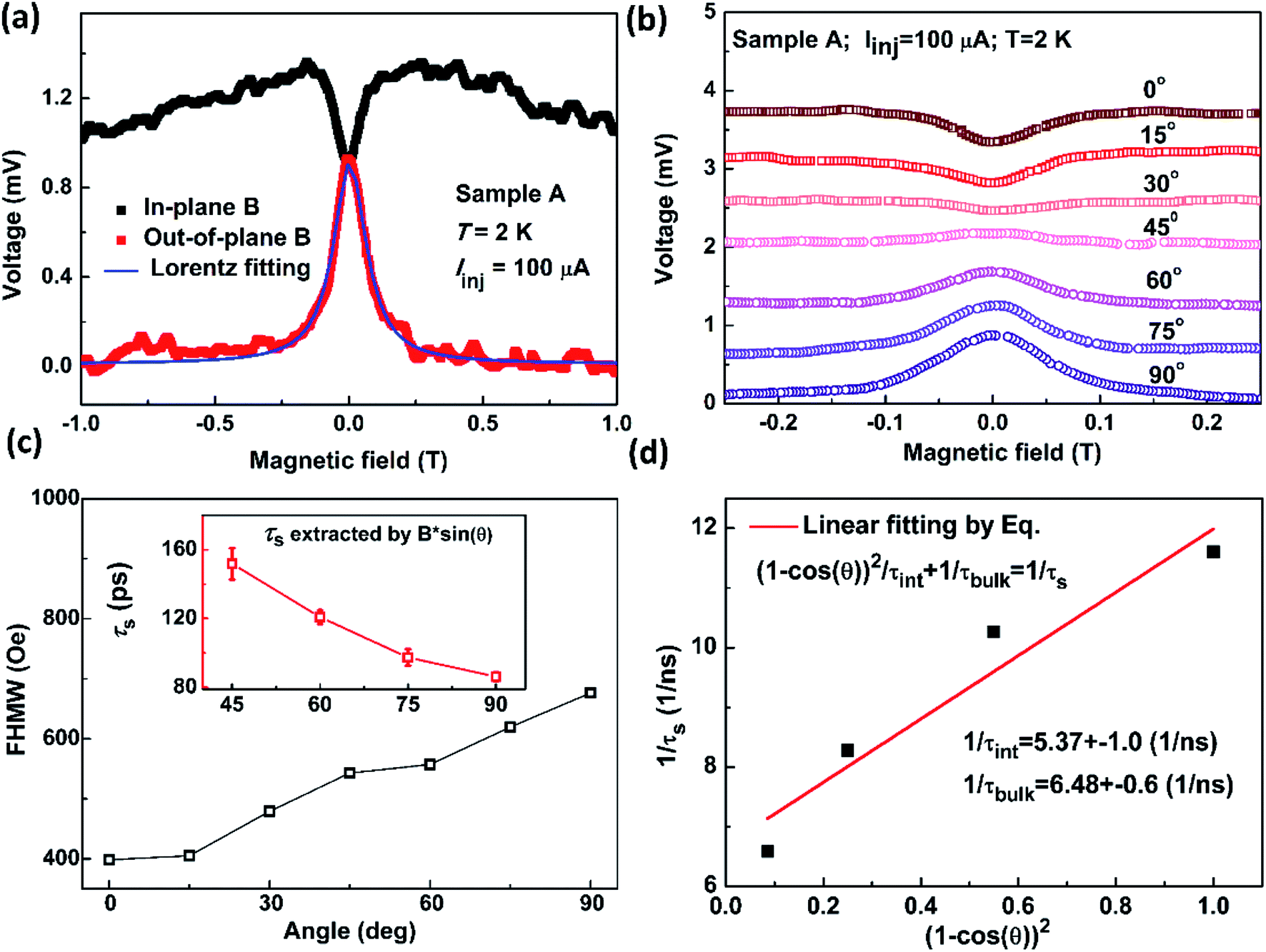 | ||
| Fig. 2 (a) The Hanle and inverted Hanle curves in sample A at 2 K. (b) The angle-dependent Hanle and inverted Hanle curves in sample A at 2 K. (c) The extracted FHMW at various angles, and the inset shows the spin relaxation time extracted from the Hanle curves (θ ≥ 45°). (d) The spin relaxation rate 1/τint and 1/τbulk are extracted by linear fitting 1/τs against (1 − cos(θ))2. | ||
 | ||
| Fig. 3 (a) The bias current-dependent τs and bias voltage in sample A. (b) The temperature-dependent Hanle curves under Iinj = 100 μA. (c) The temperature-dependent τs extracted from Hanle curves and bias voltage under Iinj = 100 μA. (d) The Hanle curve in sample A at 80 K, while the inverted Hanle curve is vanished. | ||
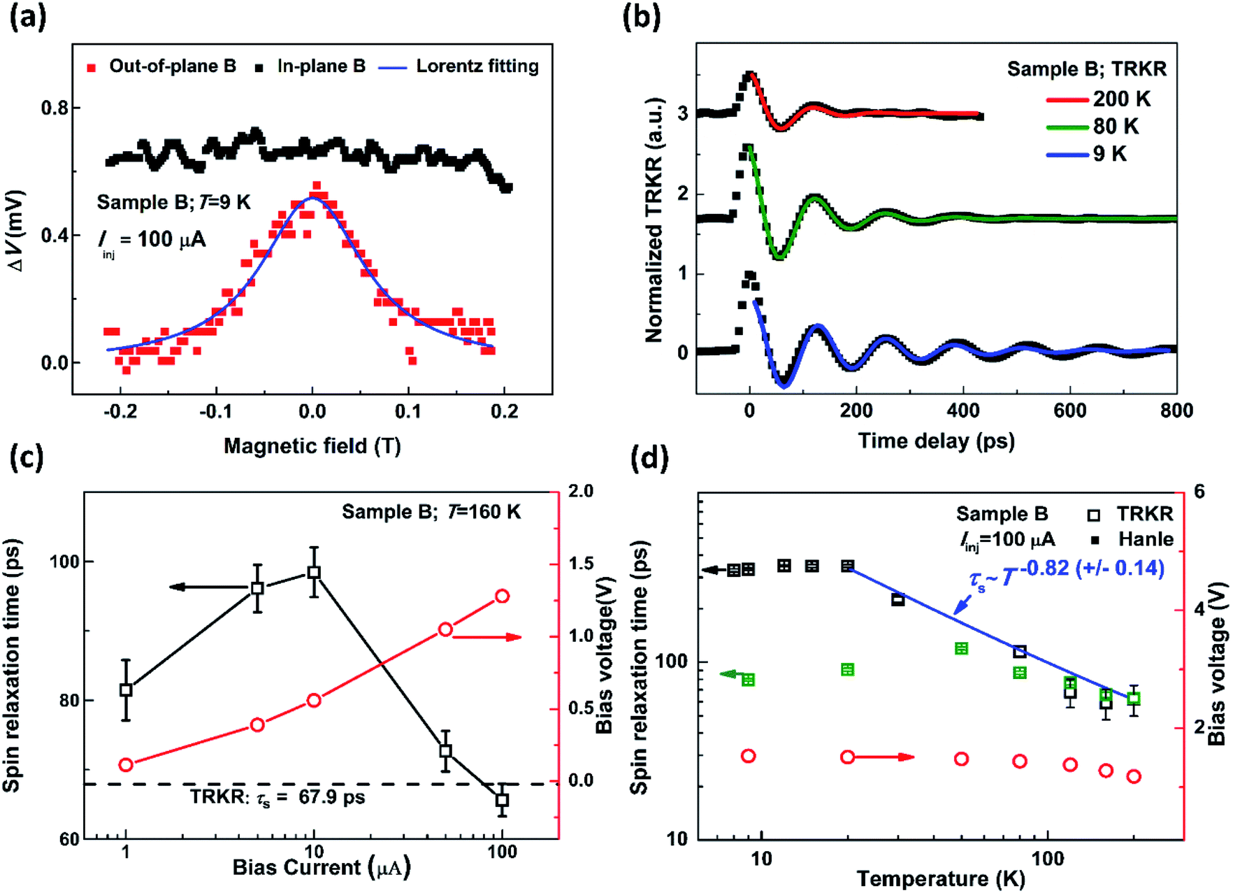 | ||
| Fig. 4 (a) The Hanle curve and vanished inverted Hanle curve in sample B at 9 K. (b) The TRKR signals under an external magnetic field at various temperatures. (c) The bias current-dependent τs and bias voltage at 160 K. The corresponding τs extracted from TRKR is also shown. (d) τs extracted by Hanle curves under Iinj = 100 μA and TRKR measurements in sample B at various temperatures. | ||
Besides of the Hanle effect, the inverted Hanle effect18,29 responding to the in-plane external magnetic field Bext,∥, was observed in sample A while absent in sample B, as shown in Fig. 2(a) and 4(a). According to ref. 18, larger roughness of the MgO/Co interface (caused by rougher GaN surface for sample A) results in an interfacial random magnetostatic field ![[capital Omega, Greek, vector]](https://www.rsc.org/images/entities/i_char_e1d9.gif) FM which can accelerate spin relaxation process. The spin relaxation rate caused by FM can be expressed as:28
FM which can accelerate spin relaxation process. The spin relaxation rate caused by FM can be expressed as:28
1/τs,int ∝ (<FM2(![[r with combining right harpoon above (vector)]](https://www.rsc.org/images/entities/i_char_0072_20d1.gif) )>) )>)
| (2) |
FM()> represents the interfacial random magnetostatic field averaged over the electron position during the injection process. The in-plane parallel field can stabilize the spin accumulation from relaxing and prolong its relaxation time and finally leads to a positive magnetic resistance (MR) as shown in Fig. 2(a). These in-plane and out-of-plane magnetic field dependence of ΔVs demonstrate build-up of spin accumulation inside n-GaN and rule out other effects, such as impurity-assisted tunnelling magnetoresistance that should be isotropic with respect to the field directions.23 In addition, the absence of the inverted Hanle effect in sample B also indicated the spin relaxation mechanism caused by FM could be ignored for sample B whose interfacial roughness was smaller than sample A.
Sample A was then utilized to investigate spin relaxation processes influenced by FM (the interfacial random magnetostatic field due to interfacial roughness). As shown in Fig. 2(b), the Hanle and inverted Hanle curves were measured at different angle θ between magnetic field and sample plane. θ was defined as shown in Fig. 1(a). As θ changed from 90° to 0°, the effect dominating spin relaxation changed from Hanle effect to inverted Hanle effect. Thus the spin voltages reversed sign with the decreased θ. The full width at half maximum (FWHM) of the Hanle curve is proportional to the spin relaxation rate (1/τs) according to eqn (1). As shown in Fig. 2(c), the extracted FWHM (τs) increases (decreases) with increasing θ. Actually, the effective external magnetic field Beffext,⊥ = Bextsin(θ) is used to extract τs from the Hanle curves (θ ≥ 45∘). The extracted τs decreases from 152 ps to 86 ps shown in the inset of Fig. 2(c).
As seen in Fig. 1(a), considering the suppression effect of Bext,∥, the θ-dependence of <FM2()> could be expressed as <FM2()> ∝ (1 − cos(θ))2. Combining eqn (2), the angle-dependent spin relaxation rate (1/τs) can be given as 1/τs = (1 − cos(θ))2/τint + 1/τbulk where 1/τint and 1/τbulk correspond to the spin relaxation rate induced by FM and spin relaxation rate induced by bulk GaN, respectively. As shown in Fig. 2(d), by linearly fitting the dependence of 1/τs on (1 − cos(θ))2, the spin relaxation rates are derived as 1/τint = 5.37 (1/ns) and 1/τbulk = 6.48 (1/ns). The results indicate that the spin relaxation caused by FM was comparable to the intrinsic contributions of bulk GaN at 2 K.
Furthermore, the T-dependent τs was extracted by electrical Hanle effect measurements in sample A. Firstly, in order to exclude influence of the localized interfacial states, the dependence of τs on bias current was measured. As shown in Fig. 3(a), τs hardly depended on the bias current, which confirmed the extracted τs was not affected by localized interfacial states. If those localized interfacial states were involved in spin transport and relaxation, noticeable bias-dependent τs would have been expected as reported in ref. 13 and 16. Then the Hanle curves were obtained at various temperatures under the same bias current. As shown in Fig. 3(b), the spin voltages ΔVs of Hanle curves decreased gradually with increasing T, and the extracted τs was shown in Fig. 3(c). The spin relaxation mechanism has been extensively studied in wurtzite bulk GaN, and the Dyakonov–Perel (DP) spin relaxation mechanism originating from the bulk SOC is regarded as the dominant one.28,30,31 In the DP scenario, the dependence of τs on T satisfies28
| τs,bulk ∝ 1/[(k1T + k3T3)τp] | (3) |
FM induced spin relaxation in low temperature region. As shown in Fig. 3(d), the inverted Hanle effect are almost negligible at 80 K, which means the dominant spin relaxation mechanism changed to DP mechanism of bulk GaN in high-temperature region. The Rashba SOC is the major contributing term for the DP mechanism in bulk GaN,28 and the T-dependence of τs satisfies τs ∝ T−1. The extracted τs ∝T −0.72±0.12, which was close to the theoretical prediction. Their discrepancy might arise due to the T-independent spin relaxation induced by FM. Since the bias voltage was kept nearly constant at different temperatures, shown in Fig. 3(c), the influence of the electron kinetic energy could be safely excluded.32
In sample A with very high doping level and large roughness, the above data indicated interface random magnetostatic field remarkably influenced spin relaxation. In the following part, instead, sample B with lower doping density and wider Schottky barrier was utilized to investigate the spin relaxation process influenced by interface band bending. Besides of the electrical Hanle effect measurements, the TRKR was used to measure the τs of the same bulk n-GaN with sample B for comparison. In addition, due to the much higher background carrier density, the signal-to-noise ratio of the TRKR results was too low to accurately extract a reliable spin relaxation time in the n-GaN of sample A. Owing to the absence of the spin injector (MgO/Co/Pt), the spin relaxation is not affected by interface band bending effect in the TRKR measurements. The TRKR signal is shown in Fig. 4(b) at various temperatures, where a double exponential cosine damped function [A1exp(−t/τc) + A2]exp(−t/τs)cos(ωt) was used to extract τs where τc represented the recombination time of photon-generated carriers.28 As shown in Fig. 4(d), the T-dependence of τs extracted from the TRKR satisfied τs ∝ T−0.82±0.14 at T higher than 20 K. With increased T, the τs increased slightly at T below 20 K, which was attributed to the T-dependent momentum scattering time.33
According to the DP spin relaxation mechanism, the lightly doped bulk GaN (sample B) has a longer τs than the highly doped one (sample A).30 This feature will lead a more sensitive dependence on FM for sample B during the electrical spin injection process. However, as shown in Fig. 4(a), the FM-related inverted Hanle effect is absent in sample B at 9 K, which confirmed that the FM induced spin relaxation is suppressed in sample B by the smoother n-GaN/Co interface.
Moreover, the dependence of τs on bias current was measured to check influence of localized interfacial states.16 As seen in Fig. 4(c), τs of sample B extracted from Hanle effect was sensitive to the bias current and became much longer under low bias current, which was different from the case of sample A. In sample A with heavy doping level, Schottky barrier was thin and therefore the MgO barrier dominated transport. However, in sample B with much lower doping level, Schottky barrier became much thicker as well and its influence could not be ignored anymore.
Considering multistep sequential tunnelling process inside Schottky barrier region via the localized interfacial states as reported in ref. 13, the effective τs extracted from Hanle measurement should be actually an averaged spin relaxation time τint of the localized interfacial states and τbulk of the bulk.13,16 Fortunately, τs is close to τint under low negative bias voltages and becomes closer to τbulk under higher negative bias voltages due to different tunnelling channels under different bias conditions.13,16,17 Under the framework of DP mechanism, the spin relaxation is mainly attributed to the fluctuation of wave vector ![[k with combining right harpoon above (vector)]](https://www.rsc.org/images/entities/i_char_006b_20d1.gif) -dependent effective magnetic field induced by SOC.28 Owing to the protection effect of the potential well surrounding the interfacial defects, the fluctuation is suppressed and τint is normally longer than τbulk,13,16 which results in the longer τs under low bias voltages as in our case.
-dependent effective magnetic field induced by SOC.28 Owing to the protection effect of the potential well surrounding the interfacial defects, the fluctuation is suppressed and τint is normally longer than τbulk,13,16 which results in the longer τs under low bias voltages as in our case.
As shown in Fig. 4(c), however, τs measured by Hanle effect approached to the TRKR value under a larger bias current (such as τs measured at 100 μA). This feature indicated that the spin-polarized electrons escaped from the localized interfacial states into bulk region under large bias and the measured τs from Hanle effect also tended to be its bulk value. In addition, the results also confirmed that the decrease of τs at large bias voltage could not be attributed to the electron kinetic energy effect. That would make the τs extracted from the electrical Hanle effect much shorter than that in bulk conduction band (extracted by TRKR) under 100 μA, which is opposite to our experimental results.
The T-dependent τs, which was extracted from electrical injection process under the large bias current Iinj = 100 μA, is shown in Fig. 4(d). At T below 50 K, τs extracted from Hanle curves was shorter than that measured by TRKR, and approached identical with the TRKR results at higher temperatures. According to the aforementioned discussion, the spin relaxation induced by the mechanism of interfacial random magnetostatic field has been excluded for sample B due to absence of the inverted Hanle effect. It is worth noting that the interfacial Rashba SOC induced by band bending has been studied experimentally and theoretically based on MOSFET structure.19,20 Accordingly, we attributed the much shorter τs than the TRKR result at low temperatures to the interfacial Rashba SOC induced by band bending in the depletion region. In more detail, interfacial inversion symmetry breaking greatly enhanced interfacial Rashba SOC and thus spin relaxation in this depletion region, which made the τs extracted from the electrical injection process much shorter than that in bulk conduction band. Considering the T-independent bias-voltage, as shown in Fig. 4(d), the interface band bending induced Rashba SOC coulde also be regarded as T-independent. However, as indicated in ref. 16, the characteristic leakage time τLS→will introduce a temperature-dependent effect to τs. A relevant parameter τLS→ can be defined as the time of electron escaping from the interfacial depletion region into the GaN conduction band in our case. It has been observed that τLS→ (the carrier backward escape time τn) decrease (increase) with temperature due to the thermal activation.16 The shorterτLS→guarantees the weaker influence of the interface band bending on spin relaxation process. As a result, the effect of interface band bending on spin relaxation was eliminated at high temperatures, which is consistent with results in Fig. 4(d). Similarly, the nearly T-independent bias voltage also indicated that the effect of the electron kinetic energy could also be excluded.
4. Conclusions
In conclusion, the electrical spin injection into bulk n-GaN was demonstrated at temperatures from 2 K to 200 K, and spin relaxation related with interfacial effects during the electrical injection process was studied. In particular, the spin relaxation process induced by interfacial random magnetostatic field was comparable to the intrinsic contribution at low temperature for heavily doped GaN, and this effect could be suppressed by smoothening n-GaN interface for lightly doped samples. The interfacial Rashba SOC caused by band bending for the lightly doped GaN greatly enhanced spin relaxation at low temperature and could be eliminated by thermal activation at high temperatures and large bias condition both of which can help electrons escape from the interfacial depletion region. These results indicated some principles, (1) smooth surface to lower interfacial random magnetostatic field and (2) large bias condition and high temperatures to help spin-polarized electrons escape from interfacial depletion region, to engineer GaN/MgO/Co spin injectors to realize longer spin relaxation time, which could advance the development of spintronics based on wide-bandgap semiconductors.Conflicts of interest
There are no conflicts to declare.Acknowledgements
The authors would like to thank professor Yuan Lu for helpful discussions. This work was supported by National Key Research and Development Program of China (No. 2018YFB0406603, 2017YFA0206200, and 2016YFA0301202), the National Natural Science Foundation of China (No. 61574006, 61522401, 11974398, 61927806, 61521004, 11634002 and 11674311) and K. C. Wong Education Foundation, China. C. H. Wan also appreciates financial support from Youth Innovation Promotion Association, CAS (Grant No. 2020008).Notes and references
- A. Bhattacharya, M. Z. Baten, I. Iorsh, T. Frost, A. Kavokin and P. Bhattacharya, Phys. Rev. Lett., 2017, 119(6), 067701 CrossRef PubMed.
- J. Y. Chen, C. Y. Ho, M. L. Lu, L. J. Chu, K. C. Chen, S. W. Chu, W. Chen, C. Y. Mou and Y. F. Chen, Nano Lett., 2014, 14, 3130–3137 CrossRef CAS PubMed.
- S. Datta and B. Das, Appl. Phys. Lett., 1990, 56, 665–667 CrossRef CAS.
- H. C. Koo, J. H. Kwon, J. Eom, J. Chang, S. H. Han and M. Johnson, Science, 2009, 325, 1515–1518 CrossRef CAS PubMed.
- P. Chuang, S.-C. Ho, L. W. Smith, F. Sfigakis, M. Pepper, C.-H. Chen, J.-C. Fan, J. P. Griffiths, I. Farrer, H. E. Beere, G. A. C. Jones, D. A. Ritchie and T.-M. Chen, Nat. Nanotechnol., 2015, 10, 35–39 CrossRef CAS PubMed.
- A. Bhattacharya, M. Z. Baten and P. Bhattacharya, Appl. Phys. Lett., 2016, 108(4), 042406 CrossRef.
- T.-E. Park, Y. H. Park, J.-M. Lee, S. W. Kim, H. G. Park, B.-C. Min, H.-J. Kim, H. C. Koo, H.-J. Choi, S. H. Han, M. Johnson and J. Chang, Nat. Commun., 2017, 8(1), 1–7 CrossRef PubMed.
- E. I. Rashba, Phys. Rev. B: Condens. Matter Mater. Phys., 2000, 62, R16267–R16270 CrossRef CAS.
- A. Fert and H. Jaffrès, Phys. Rev. B: Condens. Matter Mater. Phys., 2001, 64(18), 184420 CrossRef.
- V. F. Motsnyi, J. De Boeck, J. Das, W. Van Roy, G. Borghs, E. Goovaerts and V. I. Safarov, Appl. Phys. Lett., 2002, 81, 265–267 CrossRef CAS.
- V. F. Motsnyi, P. Van Dorpe, W. Van Roy, E. Goovaerts, V. I. Safarov, G. Borghs and J. De Boeck, Phys. Rev. B: Condens. Matter Mater. Phys., 2003, 68(24), 245319 CrossRef.
- C. Fang, C. H. Wan, B. S. Yang, J. Y. Qin, B. S. Tao, H. Wu, X. Zhang, X. F. Han, A. Hoffmann, X. M. Liu and Z. M. Jin, Phys. Rev. B: Condens. Matter Mater. Phys., 2017, 96(13), 134421 CrossRef.
- L. Huang, H. Wu, P. Liu, X. M. Zhang, B. S. Tao, C. H. Wan, Y. Yan and X. F. Han, Appl. Phys. Lett., 2018, 113(22), 222402 CrossRef.
- A. T. Hanbicki, O. M. J. van 't Erve, R. Magno, G. Kioseoglou, C. H. Li, B. T. Jonker, G. Itskos, R. Mallory, M. Yasar and A. Petrou, Appl. Phys. Lett., 2003, 82, 4092–4094 CrossRef CAS.
- A. T. Hanbicki, B. T. Jonker, G. Itskos, G. Kioseoglou and A. Petrou, Appl. Phys. Lett., 2002, 80, 1240–1242 CrossRef CAS.
- M. Tran, H. Jaffrès, C. Deranlot, J. M. George, A. Fert, A. Miard and A. Lemaître, Phys. Rev. Lett., 2009, 102(3), 036601 CrossRef CAS PubMed.
- A. Jain, J. C. Rojas-Sanchez, M. Cubukcu, J. Peiro, J. C. Le Breton, E. Prestat, C. Vergnaud, L. Louahadj, C. Portemont, C. Ducruet, V. Baltz, A. Barski, P. Bayle-Guillemaud, L. Vila, J. P. Attané, E. Augendre, G. Desfonds, S. Gambarelli, H. Jaffrès, J. M. George and M. Jamet, Phys. Rev. Lett., 2012, 109(10), 106603 CrossRef CAS PubMed.
- S. P. Dash, S. Sharma, J. C. Le Breton, J. Peiro, H. Jaffrès, J. M. George, A. Lemaître and R. Jansen, Phys. Rev. B: Condens. Matter Mater. Phys., 2011, 84(5), 054410 CrossRef.
- T. Matsuyama, R. Kürsten, C. Meißner and U. Merkt, Phys. Rev. B: Condens. Matter Mater. Phys., 2000, 61, 15588–15591 CrossRef CAS.
- S. Lamari, Phys. Rev. B: Condens. Matter Mater. Phys., 2001, 64(24), 245340 CrossRef.
- C. Y. Hu, K. Morita, H. Sanada, S. Matsuzaka, Y. Ohno and H. Ohno, Phys. Rev. B: Condens. Matter Mater. Phys., 2005, 72(12), 121203 CrossRef.
- S. Jahangir, F. Doğan, H. Kum, A. Manchon and P. Bhattacharya, Phys. Rev. B: Condens. Matter Mater. Phys., 2012, 86(3), 035315 CrossRef.
- O. Txoperena, Y. Song, L. Qing, M. Gobbi, L. E. Hueso, H. Dery and F. Casanova, Phys. Rev. Lett., 2014, 113(14), 146601 CrossRef PubMed.
- J.-Y. Park, S.-heon C. Baek, S.-Y. Park, Y. Jo and B.-G. Park, Appl. Phys. Lett., 2015, 107(18), 182407 CrossRef.
- S. M. Sze, Semiconductor devices: physics and technology, John wiley & sons, 2008, John Wiley & Sons, INC., New York, 3rd edn, 2012, ch. 7, pp. 228–238 Search PubMed.
- S. P. Dash, S. Sharma, R. S. Patel, M. P. de Jong and R. Jansen, Nature, 2009, 462, 491–494 CrossRef CAS PubMed.
- A. V. Rodina and B. K. Meyer, Phys. Rev. B: Condens. Matter Mater. Phys., 2001, 64(24), 245209 CrossRef.
- J. H. Buß, J. Rudolph, F. Natali, F. Semond and D. Hägele, Phys. Rev. B: Condens. Matter Mater. Phys., 2010, 81(15), 155216 CrossRef.
- A. Jain, L. Louahadj, J. Peiro, J. C. Le Breton, C. Vergnaud, A. Barski, C. Beigné, L. Notin, A. Marty, V. Baltz, S. Auffret, E. Augendre, H. Jaffrès, J. M. George and M. Jamet, Appl. Phys. Lett., 2011, 99(16), 162102 CrossRef.
- J. H. Buß, J. Rudolph, S. Starosielec, A. Schaefer, F. Semond, Y. Cordier, A. D. Wieck and D. Hägele, Phys. Rev. B: Condens. Matter Mater. Phys., 2011, 84(15), 153202 CrossRef.
- J. H. Buß, J. Rudolph, F. Natali, F. Semond and D. Hägele, Appl. Phys. Lett., 2009, 95(19), 192107 CrossRef.
- S. Krishnamurthy, M. van Schilfgaarde and N. Newman, Appl. Phys. Lett., 2003, 83, 1761–1763 CrossRef CAS.
- C. Adelmann, X. Lou, J. Strand, C. J. Palmstrøm and P. A. Crowell, Phys. Rev. B: Condens. Matter Mater. Phys., 2005, 71(12), 121301 CrossRef.
| This journal is © The Royal Society of Chemistry 2020 |