DOI:
10.1039/C9RA10895E
(Paper)
RSC Adv., 2020,
10, 16776-16782
Controllable growth of three-dimensional CdS nanoparticles on TiO2 nanotubes to enhance photocatalytic activity†
Received
16th January 2020
, Accepted 6th April 2020
First published on 29th April 2020
Abstract
Exploiting photocatalysts with characteristics of low cost, high reactivity and good recyclability is a great significance for environmental remediation and energy conversion. Herein, hollow TiO2 nanotubes were fabricated by a novel and efficient method via electrospinning and an impregnation calcination method. With the hydrothermal method, the CdS nanoparticles were modified on the surface and in walls of the TiO2 nanotubes. By changing the reaction conditions, the morphology of CdS nanoparticles presents a controllable three-dimensional (3D) structure. The morphology of the samples was characterized by scanning electron microscopy (SEM) and transmission electron microscopy (TEM). The structure and components of samples were characterized by X-ray diffraction (XRD), energy dispersive X-ray analysis (EDX) and X-ray photoelectron spectroscopy (XPS). The light absorption efficiency was detected using UV-vis diffuse reflectance spectroscopy (DRS) and photoluminescence (PL). The photocatalytic properties were evaluated by degradation of methyl orange (MO) and photocatalytic hydrogen evolution under visible light irradiation. From the results, the TiO2/CdS nanotubes exhibit better photocatalytic activity than the pure TiO2. The synthetic mechanism of TiO2/CdS heterostructures and a possible photocatalytic mechanism based on the experimental results were proposed.
1 Introduction
With progress in the field of nanotechnology, it has become possible to prepare semiconducting materials of nanocrystal structures with special shapes and dimensions, such as nanofibers, nanorods, nanoflowers, nanospheres and nanotubes,1–5 which have garnered extensive attention on account of their unique electronic, optical, and photoactive properties.6–9 Meanwhile, they are widely utilized in the fields of gas sensors, optical devices, visible light detectors, and field emission emitters, especially for photocatalysis.10–15 Among copious inorganic semiconductor nanostructures, titanium oxide (TiO2) has been extensively studied to date, with extensive research on its high surface-to-volume ratio, low cost, environmental friendliness and unique physical and chemical properties.16–19 Recently, the application of TiO2 as photocatalysts for degradation of toxic organic pollutants have attracted wide public attention, because the TiO2 nanostructure and its composites can significantly improve the photocatalytic performance.20–22 The properties of nanomaterials mainly rely on their nanoscale and morphology, for nanoscale semiconductor to perform well as catalysts, they at least satisfy three characteristics: (1) high specific surface area, (2) have good stability and (3) the size and distribution should be uniform.23–25 Therefore, TiO2 nanotubes shows intrinsic advantages compared to traditional TiO2 in terms of size and specific surface area,26 design and fabricate TiO2 based nanotubes for heterogeneous photocatalysis have become a hot research topic. Thus far, many synthesis methods such as electrodeposition method, sol–gel method, template-assisted and hydrothermal treatment, have been developed for fabricating TiO2 nanotube.18,19,27,28 However, these traditional method often accompanied problems such as cumbersome operation, template hard removal, high production cost and poor structural stability, etc.29
Meanwhile, the high recombination rate of photogenerated (PG) electron/hole pairs is another limits factor of photocatalysis.30,31 Although reduce the size of nanoscale TiO2 open a convenient way for improving photocatalytic efficiency, but it cannot tackle the fundamental limits issue.32,33 By contrast, making TiO2 doped with other elements, modified with noble metal and combined with other semiconductors to form heterostructures, which provide a effective means to inhibit the recombination of PG electron/hole pairs.34–38 It is necessary to design new-type composite photocatalysts not only improve the separation of PG electron/hole pairs, but also extend the optical absorption of TiO2, thus to obtain a more efficient utilization of solar energy.39,40 Cadmium sulfide (CdS) is an excellent n-type semiconductor with an ideal band-gap energy of 2.4 eV, which could absorb the visible light radiation up to 520 nm,41,42 has been widely used as a visible light response sensitizer.34,43 By comparing the energy levels of TiO2 with CdS, which could find their analogical band structures are quite suitable to construct heterostructures and bring an effective separation of PG electron/hole pairs.44,45 Therefore, that is expected to combination the TiO2 with CdS form a heterostructure structure for overcoming the demerits that exist in TiO2 and CdS simultaneously.46
Herein, we described the fabrication of CdS decorated TiO2 nanotubes via electrospinning combined with controlled calcination and hydrothermal process. By changing the synthesis condition, the density and size of CdS on the surface (inner wall) of the TiO2 nanotubes can be controlled. The morphology and dimension of the CdS/TiO2 nanotubes were observed by the SEM and TEM. The crystal phases, optical absorption properties, elemental and chemical state were explored by XRD, DRS and XPS. Due to the formation of CdS/TiO2 heterojunction structure, the hybrid nanoparticles could reduce the recombination of PG electron–hole pairs, and the hollow nanotubes structure provides a larger specific surface area and more active sites, that the as-prepared CdS/TiO2 nanotubes significantly improved photocatalytic activity. Moreover, that may provide a new method for preparation of semiconductor heterostructure nanotubes.
2 Experimental
2.1 Materials
Polystyrene (PS, Mw ≈ 350![[thin space (1/6-em)]](https://www.rsc.org/images/entities/char_2009.gif) 000 g mol−1), tetrabutyltitanate (TBOT, 97%), cadmium nitrate [Cd(NO3)2·4H2O, 99%], thiourea (CH4N2S, 99%), absolute ethanol (C2H6O, 99%), N,N-dimethylformamide (DMF, 99%), and methyl orange (MO, 96%) were purchased from Aladdin; all of chemicals used in the experiments were analytical grade and used without further purification.
000 g mol−1), tetrabutyltitanate (TBOT, 97%), cadmium nitrate [Cd(NO3)2·4H2O, 99%], thiourea (CH4N2S, 99%), absolute ethanol (C2H6O, 99%), N,N-dimethylformamide (DMF, 99%), and methyl orange (MO, 96%) were purchased from Aladdin; all of chemicals used in the experiments were analytical grade and used without further purification.
2.2 Methods
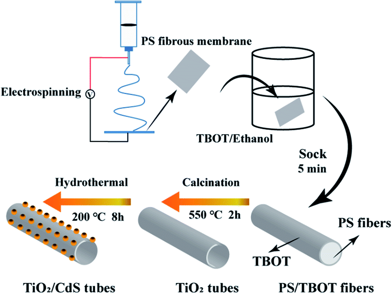
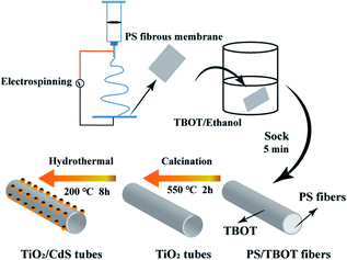
The precursor solution was prepared by adding 1.4 g PS to 5.0 mL DMF with magnetic stirring at 50 °C. After PS dissolution in the DMF completely, the prepared solution was loaded into a syringe, which was connected to a 15 kV high voltage. The flow rate of the solution was controlled at 0.5 mL h−1, and the distance from needle to the rotate acceptor was 20 cm. The whole process was kept with humidity below 20%. Then, the PS membrane were soaked in the BOT/ethanol (volume ratio 1:10) precursor solution for 5 min. Then, the composite TBOT/PS precursor fibers were natural air dried. Finally, the precursor fibers were calcined to 550 °C with a rate of 2 °C min−1 and keep 550 °C for 2 hours, to burn the PS templates completely. After annealing, the hollow TiO2 nanotubes were obtained.
Hydrothermal method was used for CdS nanoparticles modified. The as prepared TiO2 nanotubes were transferred into a Teflon-lined autoclave, which containing 30 mL solution of Cd(NO3)2 and thiourea, the concentration are equal and both volumes are 15 mL. Then, the Teflon-lined autoclave was heated to 200 °C and keep 8 hours. Finally, the CdS/TiO2 nanotubes were collected and washed in DI water. For compare the effect of reactant concentration on morphology, change the concentration of Cd(NO3)2 solution to 5, 10, 20, 30 mmol L−1 and the corresponding CdS/TiO2 nanotubes was named as TC1, TC2, TC3 and TC4, respectively (Fig. 1).
 |
| | Fig. 1 An illustration of the formation mechanism of the TiO2/CdS nanotubes. | |
2.3 Measurement of photocatalytic activity
Methyl orange (MO) was used as the target substrates for evaluating the photocatalytic activity. The photocatalytic reaction was carried out in a reactor with a circulating water system to maintain a constant temperature. The xenon lamp (Philips, 100 W) equipped with a 420 nm cut-off filter instead and the irradiation time were ranged from 5 to 200 min. Under the same conditions, all samples were placed in the quartz tube, which away from the irradiation source 5 cm. The degradation ratio was 40 mL MO solution (10 mg L−1) with 40 mg photocatalyst. Then, the suspension was stirred in the dark for 1 hour to establish adsorption and desorption equilibrium. During the photoreaction process, approximately 3 mL of the mixture was sampled in a constant time, and use centrifugation to separate the nanoparticles. The, using the spectrophotometer to determination the solution concentration. H2 evolution reactions were proceed in a closed gas-circulation system. 50 mg samples were dispersed in 200 mL aqueous solution of Na2S (1.0 M) and Na2SO3 (1.0 M). After removing the air of reaction system, the solution were irradiated by a 100 W xenon lamp equipped with a 420 nm cut-off filter, and the amount of H2 were measured by gas chromatography (GC-9700, N2 carrier).
3 Results and discussion
3.1 XRD patterns
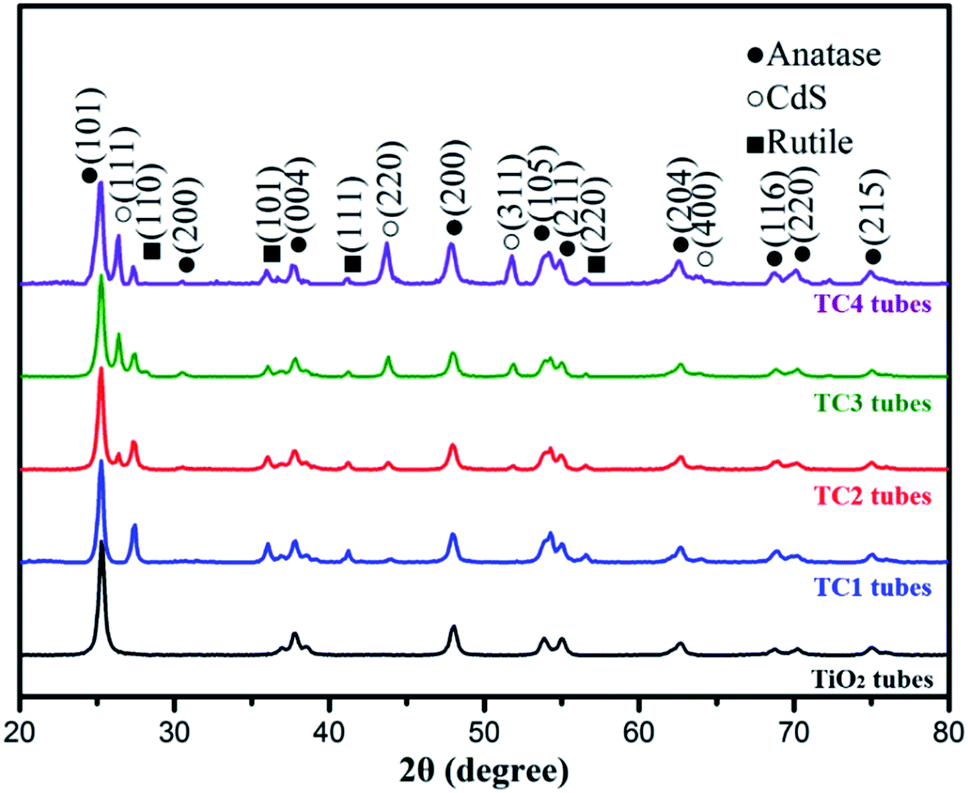
Fig. 2 present the XRD pattern of the as-prepared photocatalysts. The sharp and strong diffraction peaks showed the nanotubes were well crystallized. The main diffraction peaks of TiO2 were located at 25.45°, 37.95°, 48.20°, 55.16° and 62.81° can be indexed to the (101), (004), (200), (211) and (204) directions, respectively, which indicates that the prepared titanium oxide belongs to the anatase structure (JCPDS 21-1272), and with a high purity. Compared with pure TiO2, the CdS/TiO2 nanotubes can observe the peak at 26.52°, 43.72° confirms the formation of CdS peaks (JCPDS 65-2280), and the peaks were enhanced with increased Cd2+ concentration. Meanwhile, there is also a certain amount of rutile phase at 27.2° in the all CdS/TiO2 nanotubes. Compared the main diffraction pattern of three CdS/TiO2 nanotubes, the peaks of rutile show an decreased trend due to the addition of Cd2+, which mean the rutile may be an intermediate form of CdS/TiO2 heterogeneous structure.
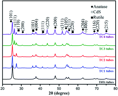 |
| | Fig. 2 The XRD patterns of the as-prepared photocatalysts. | |
3.2 Morphology of electrospun nanotubes TiO2/CdS
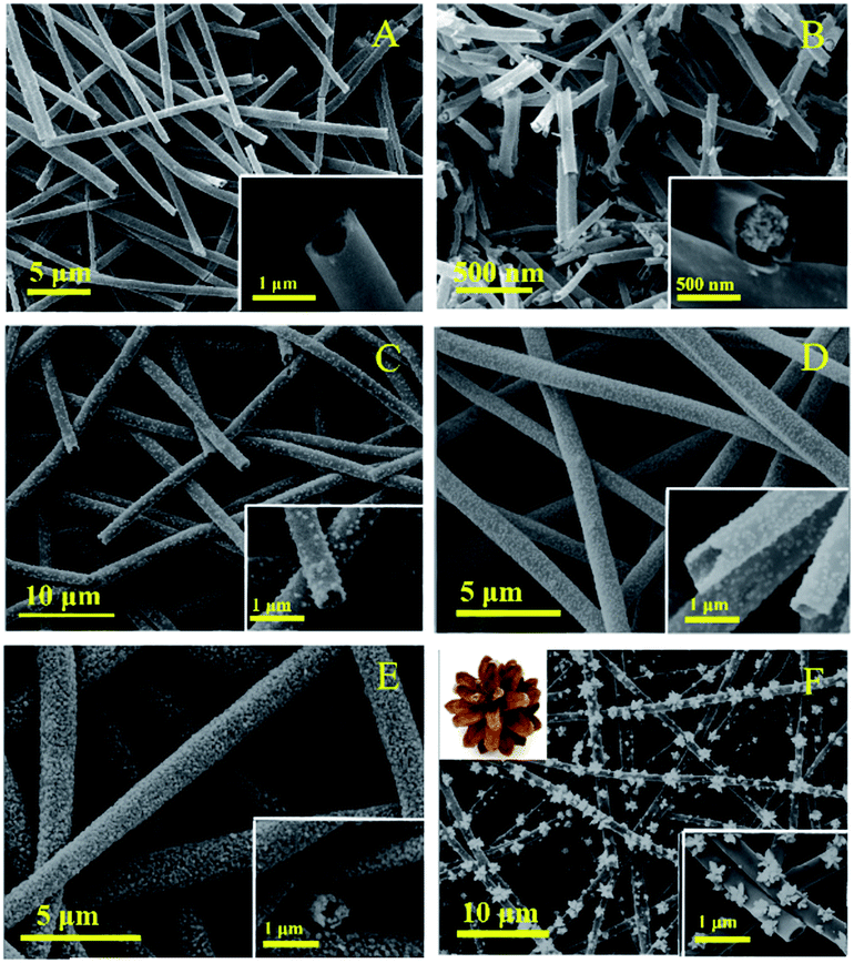
The morphology of the nanotubes were characterized by SEM. Fig. 3A show the SEM image of TiO2, which are composed by regular and uniform nanotubes with diameter of approximately 700 nm and the uniformity was above 80%, demonstrating the TBOT/ethanol solution permeate into the surface of the PS template fibers successful. From the illustration of Fig. 3A, we can observe the high magnification SEM of a TiO2 nanotube that present the wall thickness of the nanotube about 100 nm and the inwall of the nanotubes are rough. Fig. 3B clearly present the SEM image of core–shell structure TiO2 nanotubes, which was obtained by replacing PS/DMF solution with PAN/DMF solution (PAN: 13 wt%) and other operations were the same. The core might be carbon fibers which produced by the PAN incomplete calcination. The SEM of four kinds of CdS/TiO2 hybrid showed in the Fig. 3C–F with low and high magnifications. Compared to the pure TiO2 nanotubes, the CdS/TiO2 nanotubes could observed amount of nanoparticles deposited on the surface and inwall, and the density of nanoparticles increase with the concentration of Cd2+ ions. These results show that the morphology of CdS modified on the nanotubes was related to the solution concentration. Notably, further increase of Cd2+, the CdS nanoparticles grown together to form a pine-cone shaped 3D structure as shown in Fig. 3F. The morphology and microstructure of as-prepared photocatalysts also investigated by TEM. The low magnification TEM image (Fig. 4B) further verifies that CdS nanoparticles were well covered the surface and inwall of TiO2 nanotubes, compared to the TEM of TiO2 nanotubes (Fig. 4A). These nanoparticles with sizes of 5–50 nm are distributed randomly on the TiO2. The high resolution TEM image (Fig. 4D) clearly reveals an intimate interface between the TiO2 and CdS in the composite to form heterojunctions, which is favorable for the electron transfer in photocatalytic activity. Also demonstrates the CdS/TiO2 photocatalyst obtained by hydrothermal method form a heterostructure rather than a mixture of TiO2 and CdS. Meanwhile, the high resolution TEM are carried out to survey the lattice fringes of CdS/TiO2 nanotubes, the lattice spacing are 0.35 nm and 0.33 nm, which are coincident with the (101) spacing of anatase TiO2 and (111) of CdS phase. The legible fringe also suggests the high degree of crystallinity corresponds with the result of XRD results. The Fig. 4E illustrates the selected area electron diffraction (SAED) pattern of TiO2/CdS, which presentation a bright diffraction rings assigned to high crystallization and polycrystalline structure. The Fig. 4F was SAED pattern of pure CdS nanoparticles on the surface of TC3 means the obtained CdS particles were pure single crystals.
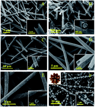 |
| | Fig. 3 The SEM images of the samples: (A) TiO2 nanotubes, (B) core–shell structure TiO2 nanotubes, (C) TC1 nanotubes, (D) TC2 nanotubes, (E) TC3 nanotubes and (F) TC4 nanotubes. | |
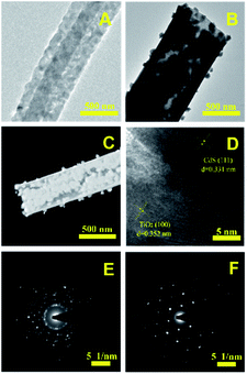 |
| | Fig. 4 The TEM image of TiO2 nanotubes (A) and TC3 nanotubes (B), the STEM image of TC3 nanotubes (C) and the HRTEM of TC3 nanotubes (D), the SAED pattern of the TC3 (E) and the CdS Nps of the surface of TC3 (F). | |
3.3 XPS analysis
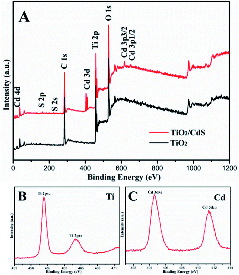
XPS analyze could reveal the information about the surface composition and chemical state. As shown in Fig. 5A, CdS/TiO2 hybrid (TC2) is mainly composed of five elements, which is Ti, O, Cd, S and C, The peak of C 1s can be ascribed to the hydrocarbon from the instrument itself. The high resolution spectra of Ti 2p were exhibited in the Fig. 5B. The Ti 2p spectra shows the peaks at 458.3 eV and 464.1 eV for Ti 2p3/2 and Ti 2p1/2 of TiO2, respectively. The distance between the two peaks is 5.8 eV, which is identical to that of the neat TiO2 indicating that Ti ion is in the form of Ti4+, high resolution spectrum of Cd 3d (Fig. 4C) displayed characteristic peaks of 404.5 eV and 411.4 eV, which are corresponding to the Cd 3d5/2 and Cd 3d3/2 states of Cd2+ in CdS, respectively. Consequently, XPS analysis further determines the formation of TiO2 and CdS in the sample, which is agreement with XRD and TEM result.
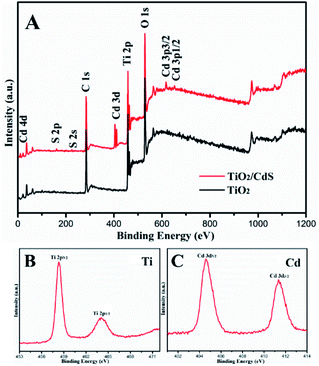 |
| | Fig. 5 The XPS spectra of the TiO2 and TC3 nanotubes: full spectrum of the sample (A), the Ti 2p spectrum (B) and Cd 3d spectrum (C). | |
3.4 UV-vis diffuse reflection spectra and PL spectra
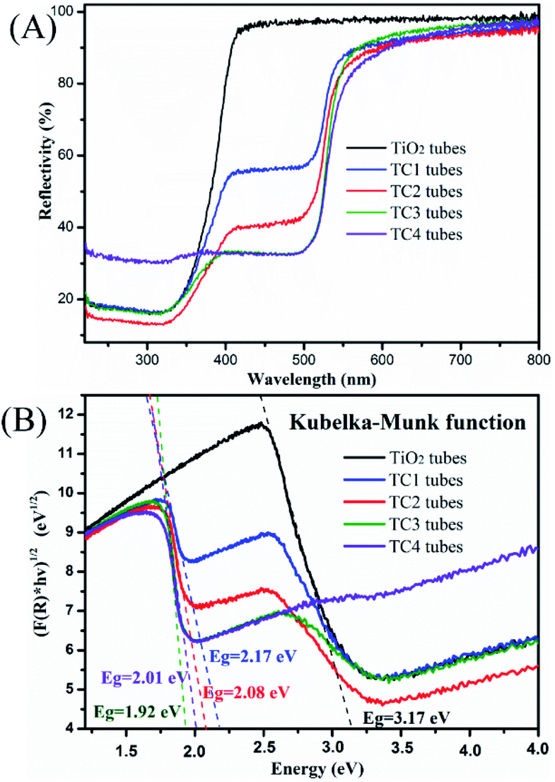
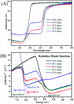
UV-vis DRS are tested to determine the optical properties of the photocatalysts. From the results of DRS (Fig. 6A) the reflection spectra of TiO2 and CdS/TiO2 heterostructure in the region spanning from 230 to 800 nm were showed. Compared to the TiO2 nanotubes, the TC2 had a lower reflectivity in the range of 240–380 nm, especially in the ultraviolet light range. After the modified of CdS, all CdS/TiO2 nanotubes present a remarkable light adsorption into the visible light region, which may due to the excellent visible-light photoresponse of CdS nanoparticles. Notably, the adsorption edges of CdS/TiO2 nanotubes gradually broaden with the mount of modified CdS nanoparticles increasing, indicated the high responsiveness of the photocatalyst to visible light.
 |
| | Fig. 6 (A) The UV-vis diffuse reflection spectra (DRS) of the as-prepared photocatalysts and (B) Kubelka–Munk transformed reflectance spectra. | |
Fig. 6B is the forbidden bandwidth obtained by the catalyst according to the Kubelka–Munk formula. Among them, the forbidden band widths of TiO2 and four CdS/TiO2 heterostructures (TC1, TC2, TC3 and TC4) are 3.17 eV, 2.17 eV, 2.08 eV, 1.92 eV and 2.01 eV. It can be seen from the comparison with the TiO2 tubes that the forbidden bandwidth of the CdS/TiO2 heterostructure is significantly reduced. Among them, TC3 has the lowest forbidden bandwidth. We can speculate that this sample has the best catalytic performance, and the catalytic experiments proved that the prediction was correct. (The detailed content of the edge position is Fig. S1.†)
3.5 Photoluminescence analysis
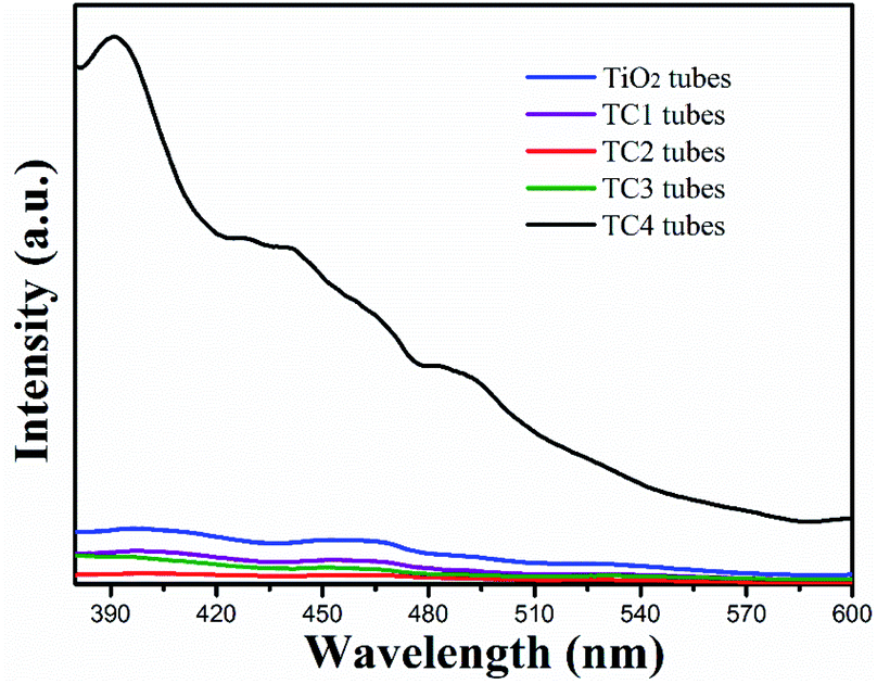
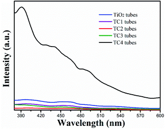
PL spectroscopy is correlation with the separation and recombination of PG electrons/holes. As shown in Fig. 7, the PL spectra of the TiO2 nanotubes showed a strong emission peak at 390 nm (excitation wavelength: 370 nm). However, the PL peak intensity of CdS/TiO2 nanotubes was significantly decreased with modification amount of CdS nanoparticles increased. The key factor in the formation of this phenomenon is the defects in the crystal structure of TiO2, which act as traps for capturing the photo-excited electrons and thus, inhibit the recombination of the electrons and holes pairs.
 |
| | Fig. 7 The photoluminescence spectra of the as-prepared photocatalysts. | |
3.6 Photocatalytic activity and recycled photocatalytic degradation performance
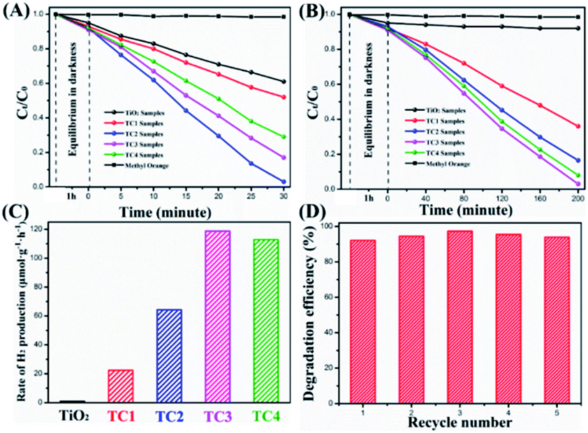
To identify the photocatalytic of the as-prepared samples, MO solution degradation were tested under UV and visible irradiation. The photocatalytic effect was evaluated by C0/Ct (C0 nd Ct were the initial concentration and the concentration of MO at time t, respectively). From the Fig. 8A, shows the concentration change of MO in the process of photodegradation, after irradiated by UV light for 30 min, the photocatalytic degradation efficiencies of the TC2 nanotubes are 95.3% slightly better than the TC3 (83.2%), which is much higher than the TC4 (72.5%) and pure TiO2 nanotubes (37.8%). The photodegradation of MO without catalysis almost negligible. However, as shown in Fig. 8B, under visible light irradiation (λ > 420 nm) for 200 minutes the TC3 shows the excellent visible light catalysis (95.2%) similar to the TC4 (94.7%), which CdS load looks like pine-cone shaped and much higher than TC2 (82.6%), TC1 (61.2%), and pure TiO2 nanotubes (0.09%), which was consistent with the results of UV-vis DRS. In addition, we also investigated the photocatalytic stability of TiO2/CdS heterostructure (TC3) under visible light irradiation. The results indicated that the hybrids exhibited good stability after being reused for five times (Fig. 8D).
 |
| | Fig. 8 Degradation rates of as-prepared photocatalysts under the UV-light (A); degradation rates of as-prepared photocatalysts under the visible light (B); the rate of H2 evolution on TiO2/CdS nanotubes under visible light (C); the repeatability tests studied on the TC3 nanotubes for five recycles (D). | |
Meanwhile, the photocatalytic activities of the nanotubes were evaluated by H2 production experiment under the visible light irradiation in aqueous solution (containing 1.0 M Na2SO3 and 1.0 M Na2S as sacrificial reagents). Fig. 8C shows the H2 evolution rate by the TiO2 and TiO2/CdS nanotubes, and there is no appreciable H2 was observed when TiO2 nanotubes was tested. In contrast, the TC1 exhibited a slightly enhanced H2 evolution rate of 22.35 μmol g−1 h−1. With the increase of CdS, the H2 evolution rate are increased. The H2 evolution rate of TC2 photocatalyst is 64.26 μmol g−1 h−1 and TC3 (118.73 μmol g−1 h−1) reaches a maximum H2 evolution rate, demonstrates that is effective to employ CdS as cocatalyst for improving efficiency of TiO2 photocatalytic activity. Further increases the amount of modification of CdS, the H2 generation rate (TC4 112.86 mol g−1 h−1) showed a slight decrease. This might be due to the less exposed active sites of TiO2/CdS resulting from the excess CdS shielding.
3.7 Mechanism for the enhancement of photocatalytic activity
The principle of photocatalytic decomposition over CdS/TiO2 heterostructure is delineated in Fig. 9. Under the visible-light irradiation, the charge carriers were firstly generated from CdS owing to its narrow energy band gap. The photoexcited electrons on the valence band (VB) of CdS can move to their own conduction band (CB). However, the high recombination of electrons (e−) and holes (h+) of CdS limits its photocatalytic activity. When the TiO2 and CdS form a heterostructure, the PG e− on CdS nanoparticles can easily transfer to the CB of TiO2 through the interface as a result of the lower conduction edge potential of TiO2 than that of CdS. Meanwhile, the h+ remain on the VB of CdS. Therefore, the TiO2 acts as a temporary e− trap to decrease the recombination of PG e−/h+. Consequently, the PG h+ on the VB of CdS can react with the surface adsorbed H2O to generate ·OH. The e− on the CB of TiO2 could reduce the adsorbed O2 to form ·O2−. Organic dye (MO) are eventually oxidized by these highly active species to CO2 and H2O products. The major reaction steps are revealed as follows:| | | TiO2/CdS + hv → TiO2/CdS (e− + h+) | (1) |
| | | TiO2/CdS (e− + h+) → TiO2 (e−) + CdS (h+) | (2) |
| | | e− + ·O2− + H+ → ·OH + OH− | (4) |
| | | ·OH + organic → other products → CO2 + H2O | (6) |
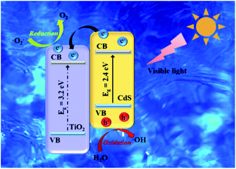 |
| | Fig. 9 Schematic diagram for the photocatalytic mechanism of the TiO2/CdS catalysts under visible-light irradiation. | |
4 Conclusions
In summary, hollow TiO2 nanotubes were obtained using electrospinning combined with an impregnation calcination method. CdS nanoparticles were modified on the surface and inner wall of TiO2 nanotubes via hydrothermal process. By changing the reaction conditions, the size and density of CdS on the surface and inner wall of the TiO2 nanotubes can be controlled. Owing to the formation of heterojunction structure, the hybrid nanoparticles could enhanced separation of e−/h+ pairs and reduce the recombination of charge carriers, and the hollow nanotubes structure provides a larger specific surface area and more active sites, that the CdS/TiO2 nanotubes showed remarkably photocatalytic activity than pure TiO2. Moreover, that may provide a new method for preparation of heterostructure nanotubes.
Conflicts of interest
No conflicts of interest in this article.
Acknowledgements
This study was supported by the Special Health Project of Jilin Province, China (No. 3D516D703429) and the Special Health Project of Department of Finance of Jilin Province, China (No. 3D5177703429).
References
- L. Zhang, Z. Q. Cheng, D. F. Wang and J. F. Li, Mater. Lett., 2015, 158, 439–441 CrossRef CAS.
- G. Jiang, R. Wang, X. Wang, X. Xi, R. Hu, Y. Zhou, S. Wang, T. Wang and W. Chen, ACS Appl. Mater. Interfaces, 2012, 4, 4440–4444 CrossRef CAS PubMed.
- J. N. Li, Z. Q. Cheng, M. Z. Liu, M. Y. Zhang, M. J. Hu, L. Zhang, H. F. Jiang and J. F. Li, J. Appl. Polym. Sci., 2015, 132, 41627–41635 Search PubMed.
- J. Di, J. X. Xia, M. X. Ji, B. Wang, X. W. Li, Q. Zhang, Z. G. Chen and H. M. Li, ACS Sustainable Chem. Eng., 2016, 4, 136–146 CrossRef CAS.
- R. Zamiri, B. Singh, M. S. Belsley and J. M. F. Ferreira, Ceram. Int., 2014, 40, 6031–6036 CrossRef CAS.
- W. Tian, T. Y. Zhai, C. Zhang, S. L. Li, X. Wang, F. Liu, D. Q. Liu, X. K. Cai, K. Tsukagoshi, D. Golberg and Y. Bando, Adv. Mater., 2013, 25, 4625–4630 CrossRef CAS PubMed.
- Z. Q. Cheng, S. Z. Zhao, L. J. Kang, M. T. Li and Z. L. Gao, Mater. Lett., 2018, 214, 80–83 CrossRef CAS.
- Y. A. Zhang, C. X. Wang, Z. M. Yuan, L. Y. Zhang and L. W. Yin, Eur. J. Inorg. Chem., 2017, 2281–2288, DOI:10.1002/ejic.201601535.
- Q. Tang, X. F. Meng, Z. Y. Wang, J. W. Zhou and H. Tang, Appl. Surf. Sci., 2018, 430, 253–262 CrossRef CAS.
- H. Chen, X. X. Wang, J. X. Li and X. K. Wang, J. Mater. Chem. A, 2015, 3, 6073–6081 RSC.
- J. M. Du, H. M. Wang, M. K. Yang, K. D. Li, L. X. Zhao, G. Y. Zhao, S. J. Li, X. L. Gu, Y. L. Zhou, L. Wang, Y. T. Gao, W. M. Wang and D. J. Kang, Electrochim. Acta, 2017, 250, 99–107 CrossRef CAS.
- S. H. Hwang, J. Song, Y. Jung, O. Y. Kweon, H. Song and J. Jang, Chem. Commun., 2011, 47, 9164–9166 RSC.
- B. X. Li, B. S. Zhang, S. B. Nie, L. Z. Shao and L. Y. Hu, J. Catal., 2017, 348, 256–264 CrossRef CAS.
- D. Lin, H. Wu and W. Pan, Adv. Mater., 2007, 19, 3968–3972 CrossRef CAS.
- J. A. Park, J. Moon, S. J. Lee, S. H. Kim, H. Y. Chu and T. Zyung, Sens. Actuators, B, 2010, 145, 592–595 CrossRef CAS.
- F. L. Zhang, Z. Q. Cheng, L. J. Kang, L. Y. Cui, W. Liu, X. J. Xu, G. H. Hou and H. J. Yang, RSC Adv., 2015, 5, 32088–32091 RSC.
- X. F. Wang, O. Kitao, E. Hosono, H. S. Zhou, S. Sasaki and H. Tamiaki, J. Photochem. Photobiol., A, 2010, 210, 145–152 CrossRef CAS.
- J. T. Yan, S. Y. Gao, C. L. Wang, B. Chai, J. F. Li, G. S. Song and S. Z. Chen, Mater. Lett., 2016, 184, 43–46 CrossRef CAS.
- C. S. Niu, J. S. Meng, X. P. Wang, C. H. Han, M. Y. Yan, K. N. Zhao, X. M. Xu, W. H. Ren, Y. L. Zhao, L. Xu, Q. J. Zhang, D. Y. Zhao and L. Q. Mai, Nat. Commun., 2015, 6, 7402–7410 CrossRef PubMed.
- F. X. Xiao, ACS Appl. Mater. Interfaces, 2012, 4, 7054–7062 Search PubMed.
- F. L. Zhang, Z. Q. Cheng, L. Y. Cui, T. T. Duan, A. Anan, C. F. Zhang and L. J. Kang, RSC Adv., 2016, 6, 1844–1850 RSC.
- F. L. Zhang, Z. Q. Cheng, L. J. Kang, L. Y. Cui, W. Liu, G. H. Hou, H. J. Yang and X. J. Xu, RSC Adv., 2014, 4, 63520–63525 RSC.
- D. D. Lin, H. Wu, R. Zhang and W. Pan, Chem. Mater., 2009, 21, 3479–3484 CrossRef CAS.
- G. H. Hou, Z. Q. Cheng, L. J. Kang, X. J. Xu, F. L. Zhang and H. J. Yang, Crystengcomm, 2015, 17, 5496–5501 RSC.
- S. Z. Zhao, Z. G. Cheng, L. J. Kang, Y. Y. Zhang and X. D. Zhao, Mater. Lett., 2016, 182, 305–308 CrossRef CAS.
- J. J. Liu and B. Cheng, Appl. Surf. Sci., 2018, 430, 348–354 CrossRef CAS.
- D. Yang, H. J. Zou, Y. Z. Wu, J. F. Shi, S. H. Zhang, X. D. Wang, P. P. Han, Z. W. Tong and Z. Y. Jiang, Ind. Eng. Chem. Res., 2017, 56, 6247–6255 CrossRef CAS.
- C. L. Wang, X. Tan, J. T. Yan, B. Chai, J. F. Li and S. Z. Chen, Appl. Surf. Sci., 2017, 396, 780–790 CrossRef CAS.
- Y. P. Huang, Y. E. Miao, L. S. Zhang, W. W. Tjiu, J. S. Pan and T. X. Liu, Nanoscale, 2014, 6, 10673–10679 RSC.
- J. P. Wang, J. K. Cong, H. Xu, J. M. Wang, H. Liu, M. Liang, J. K. Gao, Q. Q. Ni and J. M. Yao, ACS Sustainable Chem. Eng., 2017, 5, 10633–10639 CrossRef CAS.
- X. J. Zhou, C. L. Shao, X. H. Li, X. X. Wang, X. H. Guo and Y. C. Liu, J. Hazard. Mater., 2018, 344, 113–122 CrossRef CAS PubMed.
- S. Z. Zhao, Z. Q. Cheng, L. J. Kang, M. T. Li and Z. L. Gao, RSC Adv., 2017, 7, 50064–50071 RSC.
- X. J. Zhou, G. Zhang, C. L. Shao, X. H. Li, X. Jiang and Y. C. Liu, Ceram. Int., 2017, 43, 15699–15707 CrossRef CAS.
- L. Wu, J. C. Yu and X. Z. Fu, J. Mol. Catal. A: Chem., 2006, 244, 25–32 CrossRef CAS.
- N. Irannejad, B. Rezaei, A. A. Ensafi and M. M. Momeni, Electrochim. Acta, 2017, 247, 764–770 CrossRef CAS.
- B. X. Li, Y. G. Hao, B. S. Zhang, X. K. Shao and L. Y. Hu, Appl. Catal., A, 2017, 531, 1–12 CrossRef CAS.
- H. Wei, W. A. McMaster, J. Z. Y. Tan, L. Cao, D. H. Chen and R. A. Caruso, J. Phys. Chem. C, 2017, 121, 22114–22122 CrossRef CAS.
- J. Gao, Y. Zhou, Z. S. Li, S. C. Yan, N. Y. Wang and Z. G. Zou, Nanoscale, 2012, 4, 3687–3692 RSC.
- Z. Q. Cheng, S. Z. Zhao, Z. L. Han, Y. Y. Zhang, X. D. Zhao and L. J. Kang, Crystengcomm, 2016, 18, 8756–8761 RSC.
- H. Wang, Y. H. Liang, L. Liu, J. S. Hu and W. Q. Cui, J. Hazard. Mater., 2018, 344, 369–380 CrossRef CAS PubMed.
- J. Fu, G. N. Li, F. N. Xi and X. P. Dong, Chem. Eng. J., 2012, 180, 330–336 CrossRef CAS.
- J. R. Ran, J. G. Yu and M. Jaroniec, Green Chem., 2011, 13, 2708–2713 RSC.
- B. Pant, M. Park, H. Y. Kim and S. J. Park, J. Alloys Compd., 2017, 699, 73–78 CrossRef CAS.
- F. Y. Tian, D. F. Hou, F. C. Hu, K. Xie, X. Q. Qiao and D. S. Li, Appl. Surf. Sci., 2017, 391, 295–302 CrossRef CAS.
- J. Fu, B. B. Chang, Y. L. Tian, F. N. Xi and X. P. Dong, J. Mater. Chem. A, 2013, 1, 3083–3090 RSC.
- Y. L. Tian, J. Fu, B. B. Chang, F. N. Xi and X. P. Dong, Mater. Lett., 2012, 81, 95–98 CrossRef CAS.
Footnote |
| † Electronic supplementary information (ESI) available. See DOI: 10.1039/c9ra10895e |
|
| This journal is © The Royal Society of Chemistry 2020 |
Click here to see how this site uses Cookies. View our privacy policy here. 
 Open Access Article
 This Open Access Article is licensed under a
  *b
*b