DOI:
10.1039/C9RA10711H
(Paper)
RSC Adv., 2020,
10, 5134-5145
Effect of Mn2+ substitution on the structure, properties and HER activity of cadmium phosphochlorides†
Received
19th December 2019
, Accepted 22nd January 2020
First published on 31st January 2020
Abstract
Cadmium phosphochlorides, Cd4P2Cl3 and Cd7P4Cl6, possess cadmium atoms differently bonded to chlorine and phosphorus ligands. A combined experimental and theoretical study has been carried out to examine the effect of manganese substitution in place of cadmium in these compounds. Experimentally it is found that manganese prefers the Cd7P4Cl6 phase over Cd4P2Cl3. First-principles calculations reveal, stabilization of Cd7P4Cl6 upon Mn-substitution with a significant reduction in the formation energy when Mn2+ is substituted at Cd-sites coordinated octahedrally by Cl-ligands. Substitution of Mn2+ at two different Cd-sites in these compounds not only alters their formation energy differently but also causes a notable change in the electronic structures. In contrast to n-type conductivity in pristine Cd7P4Cl6, Mn2+ substituted Cd7−yMnyP4Cl6 analogues exhibit p-type conductivity with a remarkable enhancement in the photochemical HER activity and stability of the system. Photochemical properties of pristine and substituted compounds are explained by studying the nature of charge carriers and their dynamics.
Introduction
Cadmium phosphochlorides constitute a series of II–V–VII ternary semiconductors with novel bonding of P and Cl atoms with Cd-centres.1,2 Accordingly, besides different structural features, cadmium phosphochlorides also exhibit interesting electronic band structures and photophysical properties. We have shown recently how the variation in the Cl/Cd and P/Cd ratios in these compounds alter the optical band gaps and electronic structures.1 Among the cadmium phosphochlorides, cubic Cd4P2Cl3, with its direct band gap of 2.2 eV and a photoluminescence band in the visible-region, is the closest analogue of CdS, wherein S2− is entirely substituted by aliovalent P3− and Cl− anions.3 We considered it interesting to examine the effect of substituting manganese in cadmium phosphochlorides, since that manganese substitution in II–VI and III–V semiconductors gives rise to significant changes in the optical and electronic properties.4–6 Thus, Kamat and co-workers have demonstrated the effect of manganese doping on the carrier dynamics and related solar cell performance in CdS quantum dots.7 Sarma and co-workers have reported the generation of white light from Mn-doped CdS nanocrystals.8 A different aspect of doping paramagnetic Mn-atoms in nonmagnetic semiconductors is to produce dilute magnetic semiconductors (DMS).4 Considering the potential of III–V semiconductors-based devices, introducing magnetic ions as a dopant opens up the possibility to explore a variety of magnetic phenomenon beyond the conventional nonmagnetic host semiconductors-based systems.5 There have also been the studies of Mn-substituted semiconductors as photocatalyst materials.9
A striking difference between cadmium phosphochlorides and other semiconductor materials is the unique structural feature of the former wherein the unit cell consists of two distinct kinds of Cd-centers bonded differently to phosphorus and chlorine, giving rise to the possibility of selectivity in Mn-substitution between the two distinct Cd-sites. We chose the thermodynamically most stable Cd4P2Cl3 which is the closest analogue of CdS, to study the effect of manganese substitution. To our surprise, we observe the formation of the low-temperature Cd7P4Cl6 phase at higher temperatures in the presence of manganese. In order to understand this phenomenon and to explore the properties of the Mn-substituted phosphochlorides, we have carried out detailed first-principles calculations along with experimental studies. Theoretical calculations indicate that substitution of manganese in place of cadmium stabilizes the phosphochlorides, Mn-substitution being more favoured in Cd7P4Cl6 than in Cd4P2Cl3. Substitution of Mn2+ at the two different Cd-sites in Cd7P4Cl6 not only affects the formation energy differently but also changes the electronic band structures in a contrasting manner. The photochemical hydrogen evolution reaction (HER) activity of p-type Cd7−yMnyP4Cl6 is vastly superior to that of the pristine material wherein Cd5.8Mn1.2P4Cl6 shows an apparent quantum yield (AQY) of 47.6%. The influence of nature of charge carriers and their mechanism of action in pristine and Mn2+ substituted analogues have been studied.
Results and discussion
Experimental results
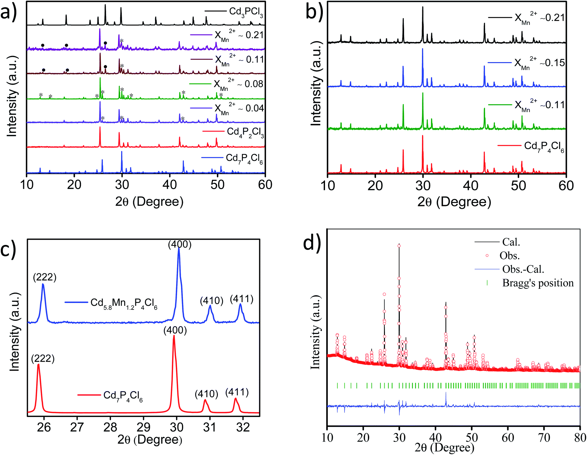
Powder X-ray diffraction (PXRD) patterns of cadmium phosphochlorides with different extent of manganese substitution are shown in Fig. 1. In the absence of MnCl2 in the precursor mixture, we obtain the thermodynamically stable Cd4P2Cl3 with the cubic structure (Pa![[3 with combining macron]](https://www.rsc.org/images/entities/char_0033_0304.gif) ). The presence of even small proportion of MnCl2 in the precursor mixture (XMn2+ = 0.04 with respect to Cd2+) affects the formation of Cd4P2Cl3 and gives rise to Cd7P4Cl6 (cubic, Pa) (∼12%) along with Cd4P2Cl3 (∼88%) (Fig. 1a). Increase in the proportion of MnCl2 (XMn2+ = 0.08) results in an increase in the Cd7P4Cl6 in the mixture from 12 to 20%. Thus, above XMn2+ of 0.08 a greenish-yellow (major product) and an orange-yellow (minor product) compound, corresponding to pure Cd7P4Cl6 and mainly Cd4P2Cl3 are formed respectively (Fig. 1a and b). Furthermore, an increase in the MnCl2 content (XMn2+ ≥ 0.15) results in the exclusive formation of pure Cd7P4Cl6 with only a trace of Cd4P2Cl3 (Fig. 1b). Comparative PXRD patterns (using zero background sample holder) of pristine Cd7P4Cl6 and Mn-substituted Cd5.8Mn1.2P4Cl6 in the selective 2θ region is shown in Fig. 1c. A right shift (towards higher 2θ) in the diffraction peaks of Cd5.8Mn1.2P4Cl6 is observed with respect to the pristine compound, indicating a decrease in the lattice parameter of the system as a result of substitution. The Rietveld refinement of Cd5.8Mn1.2P4Cl6 indeed revealed a reduction in the lattice parameter (a = 11.926 Å) with respect to the pristine Cd7P4Cl6 (a = 11.940 Å)10 which can be attributed to the smaller size of Mn2+ ions (Fig. 1d).
). The presence of even small proportion of MnCl2 in the precursor mixture (XMn2+ = 0.04 with respect to Cd2+) affects the formation of Cd4P2Cl3 and gives rise to Cd7P4Cl6 (cubic, Pa) (∼12%) along with Cd4P2Cl3 (∼88%) (Fig. 1a). Increase in the proportion of MnCl2 (XMn2+ = 0.08) results in an increase in the Cd7P4Cl6 in the mixture from 12 to 20%. Thus, above XMn2+ of 0.08 a greenish-yellow (major product) and an orange-yellow (minor product) compound, corresponding to pure Cd7P4Cl6 and mainly Cd4P2Cl3 are formed respectively (Fig. 1a and b). Furthermore, an increase in the MnCl2 content (XMn2+ ≥ 0.15) results in the exclusive formation of pure Cd7P4Cl6 with only a trace of Cd4P2Cl3 (Fig. 1b). Comparative PXRD patterns (using zero background sample holder) of pristine Cd7P4Cl6 and Mn-substituted Cd5.8Mn1.2P4Cl6 in the selective 2θ region is shown in Fig. 1c. A right shift (towards higher 2θ) in the diffraction peaks of Cd5.8Mn1.2P4Cl6 is observed with respect to the pristine compound, indicating a decrease in the lattice parameter of the system as a result of substitution. The Rietveld refinement of Cd5.8Mn1.2P4Cl6 indeed revealed a reduction in the lattice parameter (a = 11.926 Å) with respect to the pristine Cd7P4Cl6 (a = 11.940 Å)10 which can be attributed to the smaller size of Mn2+ ions (Fig. 1d).
 |
| | Fig. 1 PXRD patterns of mixed phase cadmium phosphochlorides (a), and Cd7−yMnyP4Cl6 compounds with different extents of Mn-substitution (b), comparison of major diffraction patterns of pristine Cd7P4Cl6 and Mn-substituted Cd5.8Mn1.2P4Cl6 (c), Rietveld refinement (pattern matching) pattern of Cd5.8Mn1.2P4Cl6 (d) (note: in (a), * and • represent Cd7P4Cl6, and Cd3PCl3 phases respectively). | |
In order to estimate the manganese concentration in substituted compounds, we have carried out ICP-OES measurements. Samples were thoroughly washed in H2O–C2H5OH (1![[thin space (1/6-em)]](https://www.rsc.org/images/entities/char_2009.gif) :3 volume ratio) mixture to remove the unreacted Mn-salt present on the surface. The substitution of manganese is more favoured in Cd7P4Cl6 compare to Cd4P2Cl3. Substitution of ≥12% manganese in Cd7−yMnyP4Cl6 in place of cadmium causes it to crystallize in pure form free from other compositions. We have obtained Cd7−yMnyP4Cl6 with y = 0.9–1.5, giving rise to the compositions, Cd6.1Mn0.9P4Cl6, Cd5.8Mn1.2P4Cl6, and Cd5.5Mn1.5P4Cl6 (Fig. 2a). The EDAX spectrum of Cd5.8Mn1.2P4Cl6 showed signals corresponding to Cd, Mn, P, and Cl throughout the sample, indicating uniform substitution of manganese (Fig. S1a†). An XPS scan of Cd5.8Mn1.2P4Cl6 revealed signals corresponding to Cd, Mn, P, and Cl (Fig. S1b†). High-resolution XPS-core level spectra of Cd and Mn (Fig. S1c and d†) show energy differences of 6.8 and 11.2 eV between 3d5/2 and 3d3/2 (in the case of Cd) and 2p3/2 and 2p1/2 (in the case of Mn) respectively, characteristic of Cd2+ and Mn2+ states. Phosphorus atoms in Cd7P4Cl6 form P–P dumbbell, wherein each P atom in dumbbell is bonded to 3 Cd atoms (P2Cd6 unit). The P–P bounded P atom possess a charge of (P2)4−. The crystal structure of Cd7P4Cl6 possess cationic three dimensional ∞3[Cd3P2]2+ and anionic [CdCl6]4− units and the crystallochemical formula can be written as [Cd3(P2)4−]2·[CdCl6] wherein Cd possess +2 oxidation state.10 In contrast, Cd4P2Cl3 has two different natures of phosphorus atoms wherein octahedrally coordinated (P2)4− dumbbell coexist with tetrahedrally coordinated P3− species (PCd4). The crystallochemical formula of Cd4P2Cl3 is Cd4(P3−)2(P2)4−Cl3.10 Fitting of core-level XPS signal of cadmium in pristine as well as substituted compounds reveal +2 oxidation state of cadmium and we did not observe any other Cd-species (Fig. S2†). Electron paramagnetic resonance (EPR) spectrum of Cd5.8Mn1.2P4Cl6 at room temperature showed a peak with ‘g’ value corresponding to 2.0059, confirming Mn2+ species in the compound. The absence of the hyperfine structure in the EPR spectrum is because of the high doping concentration of manganese in the host semiconductor (Fig. 2b).
:3 volume ratio) mixture to remove the unreacted Mn-salt present on the surface. The substitution of manganese is more favoured in Cd7P4Cl6 compare to Cd4P2Cl3. Substitution of ≥12% manganese in Cd7−yMnyP4Cl6 in place of cadmium causes it to crystallize in pure form free from other compositions. We have obtained Cd7−yMnyP4Cl6 with y = 0.9–1.5, giving rise to the compositions, Cd6.1Mn0.9P4Cl6, Cd5.8Mn1.2P4Cl6, and Cd5.5Mn1.5P4Cl6 (Fig. 2a). The EDAX spectrum of Cd5.8Mn1.2P4Cl6 showed signals corresponding to Cd, Mn, P, and Cl throughout the sample, indicating uniform substitution of manganese (Fig. S1a†). An XPS scan of Cd5.8Mn1.2P4Cl6 revealed signals corresponding to Cd, Mn, P, and Cl (Fig. S1b†). High-resolution XPS-core level spectra of Cd and Mn (Fig. S1c and d†) show energy differences of 6.8 and 11.2 eV between 3d5/2 and 3d3/2 (in the case of Cd) and 2p3/2 and 2p1/2 (in the case of Mn) respectively, characteristic of Cd2+ and Mn2+ states. Phosphorus atoms in Cd7P4Cl6 form P–P dumbbell, wherein each P atom in dumbbell is bonded to 3 Cd atoms (P2Cd6 unit). The P–P bounded P atom possess a charge of (P2)4−. The crystal structure of Cd7P4Cl6 possess cationic three dimensional ∞3[Cd3P2]2+ and anionic [CdCl6]4− units and the crystallochemical formula can be written as [Cd3(P2)4−]2·[CdCl6] wherein Cd possess +2 oxidation state.10 In contrast, Cd4P2Cl3 has two different natures of phosphorus atoms wherein octahedrally coordinated (P2)4− dumbbell coexist with tetrahedrally coordinated P3− species (PCd4). The crystallochemical formula of Cd4P2Cl3 is Cd4(P3−)2(P2)4−Cl3.10 Fitting of core-level XPS signal of cadmium in pristine as well as substituted compounds reveal +2 oxidation state of cadmium and we did not observe any other Cd-species (Fig. S2†). Electron paramagnetic resonance (EPR) spectrum of Cd5.8Mn1.2P4Cl6 at room temperature showed a peak with ‘g’ value corresponding to 2.0059, confirming Mn2+ species in the compound. The absence of the hyperfine structure in the EPR spectrum is because of the high doping concentration of manganese in the host semiconductor (Fig. 2b).
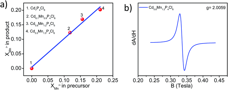 |
| | Fig. 2 (a) Mole fractions of manganese in product (obtained by ICP-OES) as a function of the mole fractions of manganese used in the precursor. (b) Room temperature EPR spectrum of Cd5.8Mn1.2P4Cl6. | |
Diffuse reflectance spectra of Mn-substituted Cd7−yMnyP4Cl6 compounds were collected in the powder form and converted into the absorbance mode employing Kubelka–Munk equation (Fig. S3a†). A small blue-shift (0.03 to 0.07 eV) occurs in the absorption spectra of Mn-substituted compounds compared to the pristine Cd7P4Cl6 (band gap ∼ 2.62 eV; λedge ∼ 472.30 nm). Tauc plots show linear behaviour between (αhν)1/n vs. hν for n = 1/2, indicating direct band gap in the compounds (Fig. S3b†).
Computational results
In order to understand the consequences of the substitution of manganese on the structural and electronic properties of cadmium phosphochlorides, we have carried out first-principles calculations. We have considered configurations with substitution of an Mn atom at two inequivalent Cd-sites in Cd7P4Cl6 and Cd4P2Cl3 to determine its effect on the structure and electronic features. Resulting compounds Cd6.75Mn0.25P4Cl6 and Cd3.875Mn0.125P2Cl3, amount to 3.6% and 3.1% Mn substitution in Cd7P4Cl6 and Cd4P2Cl3 respectively. An important difference between Cd7P4Cl6 and Cd4P2Cl3 is octahedral versus tetrahedral coordination of two kinds of Cd1 and Cd2 atoms.1,10 In Cd7P4Cl6, (a) Cd1 is distorted octahedrally coordinated with 2 P atoms and 4 Cl atoms, Cd–P bond length is 2.48 Å and a Cd–Cl bond length is 2.76 Å while the other three Cl atoms giving Cd–Cl bond lengths of 3.03 Å, 3.08 Å and 3.28 Å, and (b) Cd2 is octahedrally coordinated with 6 Cl atoms with bond lengths of 2.69 Å. In Cd4P2Cl3, (a) Cd1 is coordinated by 1 P and 3 Cl atoms with Cd–P and Cd–Cl bond lengths of 2.50 Å and 2.64 Å respectively, and (b) Cd2 is coordinated by 2 P and 2 Cl atoms with 2 Cd–P1 (Cd–P2) and Cd–Cl1 (Cd–Cl2) bond lengths of 2.49 Å (2.51 Å) and 2.85 Å (2.74 Å) respectively.1 We relaxed their structures internally upon Mn substitution until forces on each atom are less than 0.02 eV Å−1.
In Cd6.75Mn0.25P4Cl6, (a) with Mn2+ substituted at the Cd1 site (MnCd1) (Fig. 3a), Mn–P, Mn–Cl1, Mn–Cl2, Mn–Cl3 and Mn–Cl4 bond lengths are 2.47 Å, 2.42 Å, 2.50 Å, 3.50 Å and 3.69 Å (Fig. 3a and b) and (b) with Mn2+ substituted at Cd2 site (MnCd2), Mn–Cl bond length is 2.58 Å (Fig. 3c and d). In Cd3.875Mn0.125P2Cl3, (a) MnCd1, Mn–P and Mn–Cl bond lengths are 2.42 Å and 2.44 Å (Fig. 4a and b) and (b) MnCd2, Mn–P1 (Mn–P2) and Mn–Cl1 (Mn–Cl2) bond lengths are 2.43 Å (2.45 Å) and 2.44 Å (2.47 Å) (Fig. 4c and d). Clearly, there is a significant reduction in metal–X bond length with Mn2+ substitution, as expected from their ionic radii.
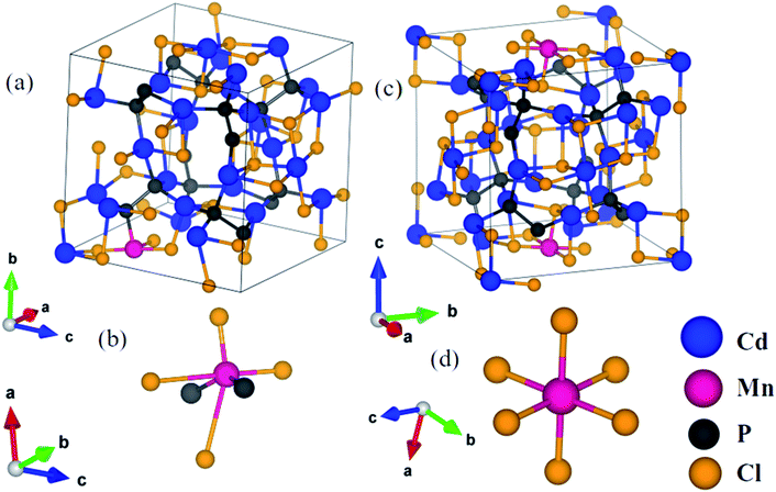 |
| | Fig. 3 Crystal structure of Mn substituted Cd7P4Cl6 at Cd1 site (a), Mn is octahedrally (distorted) coordinated with 2 P and 4 Cl atoms (b), and at Cd2 site (c) where Mn is octahedrally coordinated with Cl atoms (d). | |
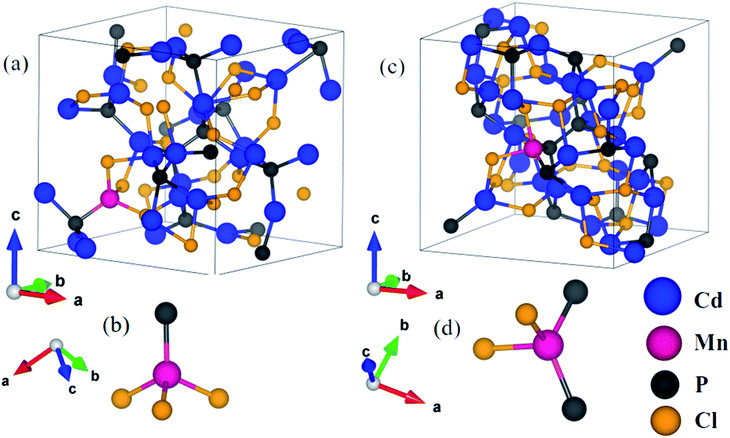 |
| | Fig. 4 Crystal structure of Cd4P2Cl3 with Mn substituted at Cd1 site (a), where Mn is tetrahedrally bonded with 1 P and 3 Cl atoms (b), and at Cd2 site (c), where Mn is tetrahedrally coordinated with 2 P and 2Cl atoms (d). | |
We estimate the formation energy (Ef) of Mn2+ substitution in Cd7P4Cl6 and Cd4P2Cl3 to find out the favourable site for Mn substitution,
| Ef = EMn–Cd1/Cd2 − EB − EMn + ECd |
where
EMn–Cd1/Cd2 and
EB are the energies of Mn-substituted and pure Cd
7P
4Cl
6 or Cd
4P
2Cl
3 phases.
EMn and
ECd are the energies of isolated Mn and Cd atoms. The difference in total energies for nonmagnetic and magnetic calculations show that the magnetic configuration is more stable than the non-magnetic one, highlighting the importance of considering spin polarization in the ground state of the system (
Table 1). We find that Mn
2+ substitution is more favourable in Cd
7P
4Cl
6 than in Cd
4P
2Cl
3 (
Table 1). In Cd
7P
4Cl
6, Mn
2+ substitution at Cd2-site is energetically more favourable than that at Cd1-site and in Cd
4P
2Cl
3, Mn
2+ substitution is more favoured at Cd1-site than that at Cd2-site. Interesting to note that in both the compounds, Mn
2+ prefers to occupy the site, which has a greater number of tightly bounded Cl-ligands. To explore the possibility of occurrence of Mn atom at the interstitial site, we introduced Mn atoms at the interstitial sites in Cd
7P
4Cl
6 and Cd
4P
2Cl
3, with coordinates (0.5, 0.5, 0.5) and (0.48, 0.88, 0.93) in Cd
7P
4Cl
6 and Cd
4P
2Cl
3 respectively (
Table 1). From their energetics, we find that Mn
2+ substitution occurs preferentially at Cd-sites, not in the interstitial sites of these compounds (
Table 1). Such preferential substitution of Cd
2+ by Mn
2+ maintains the neutrality in Mn-substituted compounds.
Table 1 Comparison of formation energies of Mn substitution Cd7P4Cl6 and Cd4P2Cl3. The difference in the energies of magnetic and non-magnetic states, and magnetic moment of Cd7P4Cl6 and Cd4P2Cl3 with Mn substitution at Cd1 and Cd2 sites. Note that in MnCd7P4Cl6 and MnCd4P2Cl3, Mn is at the interstitial site
| Compound |
Ef (eV) |
ΔE(Emag − Enon-mag) (eV) |
Magnetic moment (μB) |
| Cd6.75Mn0.25P4Cl6(MnCd1) |
−6.59 |
−2.20 |
4.43 |
| Cd6.75Mn0.25P4Cl6(MnCd2) |
−7.10 |
−2.20 |
4.61 |
| Cd3.875Mn0.125P2Cl3(MnCd1) |
−6.77 |
−2.67 |
4.47 |
| Cd3.875Mn0.125P2Cl3(MnCd2) |
−6.67 |
−2.24 |
4.40 |
| MnCd7P4Cl6 |
−3.12 |
−2.28 |
4.50 |
| MnCd4P2Cl3 |
−5.04 |
−1.58 |
3.58 |
We now examine the electronic structures of Mn2+ substituted Cd7P4Cl6 and Cd4P2Cl3 compounds and compare them with those of the pristine forms to understand the effects of substitution. Cd6.75Mn0.25P4Cl6 (MnCd1) is a direct (at Γ-point) band gap semiconductor with a gap of 1.4 eV (Fig. 5b). The band gap of Cd7P4Cl6(MnCd1) reduces by 0.4 eV upon Mn2+ substitution at Cd1 site. The states at valence band maximum (VBM) and conduction band minimum (CBM) are spin split, with VBM is constituted of spin-up states whereas CBM is constituted of spin-down states. The VBM is mainly contributed by spin-up states of P 3p orbitals whereas CBM is constituted of spin-down states of Mn-3d orbitals (Fig. 6a). Noting that Cd6.75Mn0.25P4Cl6(MnCd2) is the lowest energy configuration, we find from its electronic structure that it is a direct (at Γ-point) gap semiconductor with a band gap of 1.8 eV, without any notable change in the gap with respect to pristine Cd7P4Cl6 (Fig. 5c). In contrast to Cd6.75Mn0.25P4Cl6(MnCd1), we do not find spin split states at VBM and CBM. The VBM is mainly contributed by spin-up and spin-down states of P 3p and Cl 3p orbitals whereas CBM is constituted of spin-down states of Mn 3d orbitals (Fig. 6b). Cd3.875Mn0.125P2Cl3(MnCd1) and Cd3.875Mn0.125P2Cl3(MnCd2) are direct (at Γ-point) gap semiconductor with a band gap of 1.3 and 1.0 eV respectively (Fig. 5e and f). Mn2+ substitution in Cd4P2Cl3 at Cd2 site affects its band gap notably. From the projected density of states, VBM of Cd3.875Mn0.125P2Cl3(MnCd1) is mainly contributed by spin-up states of P 3p and Mn 3d orbitals, and CBM is constituted of spin-down states of Mn 3d orbitals (Fig. 6c). States at the VBM of Cd3.75Mn0.25P2Cl3(MnCd2) are mainly contributed by spin-up states of P 3p and Mn 3d orbitals (Fig. 6d). CBM is constituted of spin-down states of Mn 3d and 5s Cd orbitals (Fig. 6d). We find spin split states at VBM and CBM of those configurations which have Mn2+ coordinated with a greater number of P atoms, e.g., Mn2+ is octahedrally coordinated with 4 Cl and 2 P in Cd6.75Mn0.25P4Cl6(MnCd1) whereas, in Cd6.75Mn0.25P4Cl6(MnCd2), Mn is octahedrally coordinated with 6 Cl atoms (no P atoms). Similarly, Mn2+ is tetrahedrally coordinated with 3 Cl, and 1 P in Cd3.875Mn0.125P2Cl3(MnCd1) and Mn2+ is tetrahedrally coordinated with 2 P and 2 Cl in Cd3.875Mn.125P2Cl3(MnCd2). Splitting of spin-up and spin-down bands arises due to broken inversion and crystal field symmetry in the system. Cd6.75Mn0.25P4Cl6(MnCd1) exhibits spin-split states at VBM and CBM as Mn2+ is bonded to 4 Cl and 2 P atoms, forming a distorted octahedra with broken inversion symmetry (Fig. 3a). In contrast, we do not find spin split states in Cd6.75Mn0.25P4Cl6(MnCd2) since Mn2+ is bonded to 6 Cl atoms forming symmetric octahedra maintaining inversion symmetry (Fig. 3d). Similarly, Mn2+ is at the center of proper and distorted tetrahedra in Cd3.875Mn0.125P2Cl3(MnCd1) and Cd3.875Mn0.125P2Cl3(MnCd2) respectively (Fig. 4b and d). Both these compounds exhibit spin-split states at VBM and CBM; the magnitude of splitting is weak in Cd3.875Mn0.125P2Cl3(MnCd1) as the P atom is along the principal axis and 3-fold symmetry is maintained by 3 Cl atoms bonded to Mn. In Cd3.875Mn0.125P2Cl3(MnCd2), Mn2+ is bonded to 2 P and 2 Cl atoms, leading to broken 3-fold symmetry and stronger spin splitting of energy bands. Hence, Cd3.875Mn0.125P2Cl3(MnCd2) and Cd6.75Mn0.25P4Cl6(MnCd1) show spin-spit states at VBM and CBM. From the spin-resolved projected electronic density of states (DOS) (Fig. 6) of Mn2+ substituted Cd7P4Cl6 and Cd4P2Cl3 compounds, it is evident that there is a strong coupling between the Mn 3d orbitals and P 3p and Cl 3p orbitals of the host semiconductor.
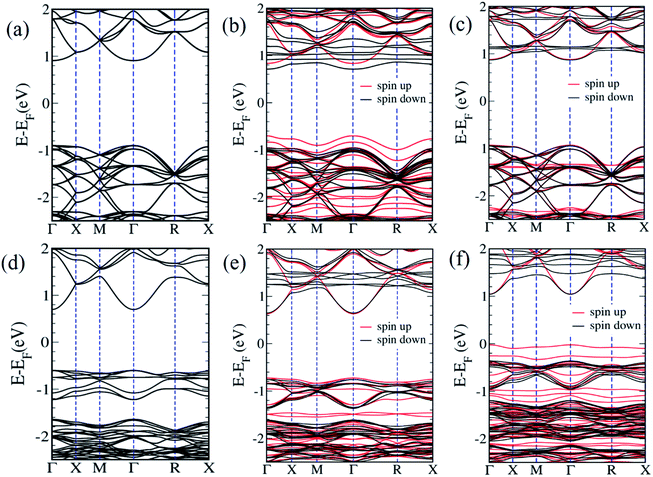 |
| | Fig. 5 Electronic structure of pristine Cd7P4Cl6 (a), Mn2+ substituted Cd7P4Cl6 at Cd1 site (b), Mn2+ substituted Cd7P4Cl6 Cd2 site (c), pristine Cd4P2Cl3 (d), Mn2+ substituted Cd4P2Cl3 at Cd1 site (e) and Mn2+ substituted Cd4P2Cl3 at Cd2 site (f). | |
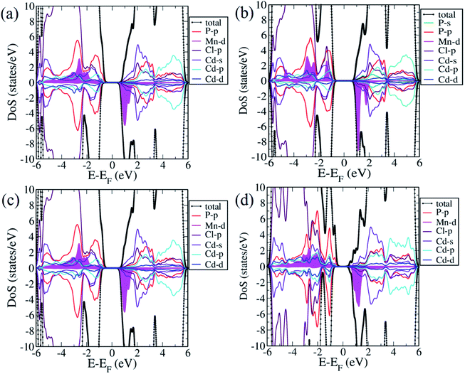 |
| | Fig. 6 Projected density of states of Cd6.75Mn0.25P4Cl6(MnCd1) (a), Cd6.75Mn0.25P4Cl6(MnCd2) (b), Cd3.875Mn0.125P2Cl3(MnCd1) (c) and Cd3.875Mn0.125P2Cl3(MnCd2) (d). Magenta color shaded area shows Mn 3d orbitals. | |
Our estimates of magnetic moments of Mn-doped Cd7P4Cl6 and Cd4P2Cl3 are tabulated in Table 1. We find that 3d orbitals of Mn are occupied as (dxy↑)1 (dyz↑)1 (dzx↑)1 (dz2↑)1 (dx2−y2↑)1, resulting in an electronic configuration with S = 5.0 μB. However, hybridizing interaction of 3d states of Mn with 3p states of Cl and P atoms results in partial cancellation of the magnetic moment μ = 5 − δ, resulting in effective local magnetic moments 4.61 μB in Cd6.75Mn0.25P4Cl6(MnCd2). Cd6.75Mn0.25P4Cl6(MnCd2) has a higher magnetic moment than of that of Mn-substituted Cd7P4Cl6 and Cd4P2Cl3 compounds.
Halogen vacancies are inherently present in cadmium phosphochlorides compounds.11 The exact composition of Cd7−yMnyP4Cl6 compounds by EDAX and XPS measurements reveal some amount of Cl and P vacancies in these compounds. We simulated Cl and P vacancies in energetically most favourable Mn2+ substituted (at Cd2 site) Cd7P4Cl6, considering 5 inequivalent configurations of vacancy pairs. In the configuration I, we removed a pair of P atoms from the crystal, each of which is bonded with three Cd1 atoms. Two Cl atoms are removed from octahedral coordination of Mn atom in configuration II, whereas one atom is removed from 6 Cl atoms bonded with Mn, and another Cl is extracted from octahedrally coordinated Cd2 atom in configuration III. Configurations IV and V have mixed pairs of Cl and P vacancies, in both cases, Cl atom is taken from octahedrally coordinated Mn atom, and P is removed from P1–P2 pair, such that the distance of Cl vacancy from P1 and P2 atoms is 5.33 Å and 3.85 Å respectively. We simulate pure Cl and P vacancy pairs in pristine Cd7P4Cl6, in the configuration I, we remove a P pair from crystal and remove 2 Cl atoms from octahedrally coordinated Cd2 atom in configuration II. From the formation energies of vacancies (Table 2), we conclude that it is relatively easy to introduce a Cl vacancy than a P vacancy in pristine as well as Mn substituted Cd7P4Cl6 compound. Secondly, it is easier to introduce P vacancy in Mn-substituted Cd7P4Cl6 compound than in the pristine one. Cl vacancies are easier to be introduced in Mn substituted Cd7P4Cl6 compound than in the pristine one when Cl atom is removed each from octahedrally coordinated Mn and Cd2 atoms rather than introducing both the vacancies at octahedrally coordinated Mn or Cd2 atom. We present the electronic structure of the configurations III and V as configuration III has the lowest defect formation energy, and configuration V has lower Ef than of I and IV configurations and understands the combined effect of Cl and P vacancies. In the electronic structure, we find that Cl and P vacancy pairs make Cd6.75Mn0.25P4Cl6(MnCd2) an indirect (Γ–R) band gap semiconductor with gaps of 1.68 eV and 1.14 eV for III and V configurations (Fig. 7a and c). Associated with Cl vacancy, we identify a new defect band on the bottom of the CBM (Fig. 7a), which is also seen in the density of states (Fig. 7b). The peak has contributions mainly from minority spin states of Cl-3p and Cd-5s orbitals. The introduction of P and Cl vacancies leads to defect bands just above the VBM and below the CBM (Fig. 7c), as evident in the density of states (Fig. 7d). Spin-up and spin-down states at VBM and CBM here are mainly contributed by P 3p, Cd 5s, and Cd 5p orbitals.
Table 2 Comparison of defect formation energies of pristine Cd7P4Cl6 and Mn-substituted Cd7P4Cl6 with different vacancy configuration
| Compound |
Vacancy configuration |
Ef (eV/vacancy) |
| Cd7P4Cl6 |
I (2 P) |
7.86 |
| Cd7P4Cl6 |
II (2 Cl) |
4.65 |
| Cd6.75Mn0.25P4Cl6(MnCd2) |
I (2 P) |
7.73 |
| Cd6.75Mn0.25P4Cl6(MnCd2) |
II (2 Cl) |
4.84 |
| Cd6.75Mn0.25P4Cl6(MnCd2) |
III (Cl–Cl) |
4.48 |
| Cd6.75Mn0.25P4Cl6(MnCd2) |
IV (Cl–P1) |
7.16 |
| Cd6.75Mn0.25P4Cl6(MnCd2) |
V (Cl–P2) |
7.00 |
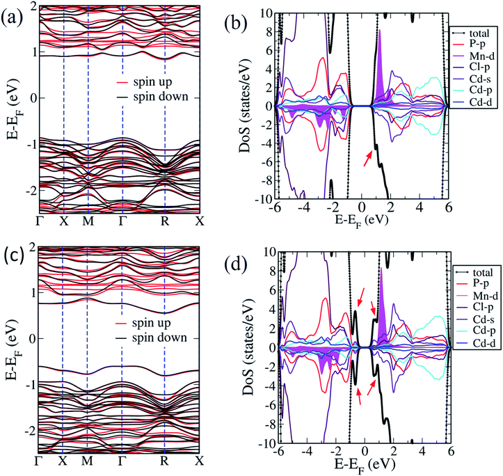 |
| | Fig. 7 Electronic structure and spin-resolved polarized projected density of states of Cd6.75Mn0.25P4Cl6(MnCd2) with Cl vacancy (a and b) and Cd6.75Mn0.25P4Cl6(MnCd2) with Cl–P2 vacancies (c and d). Note that defect peaks are marked by the red arrow in the projected density of states. | |
Photochemical studies
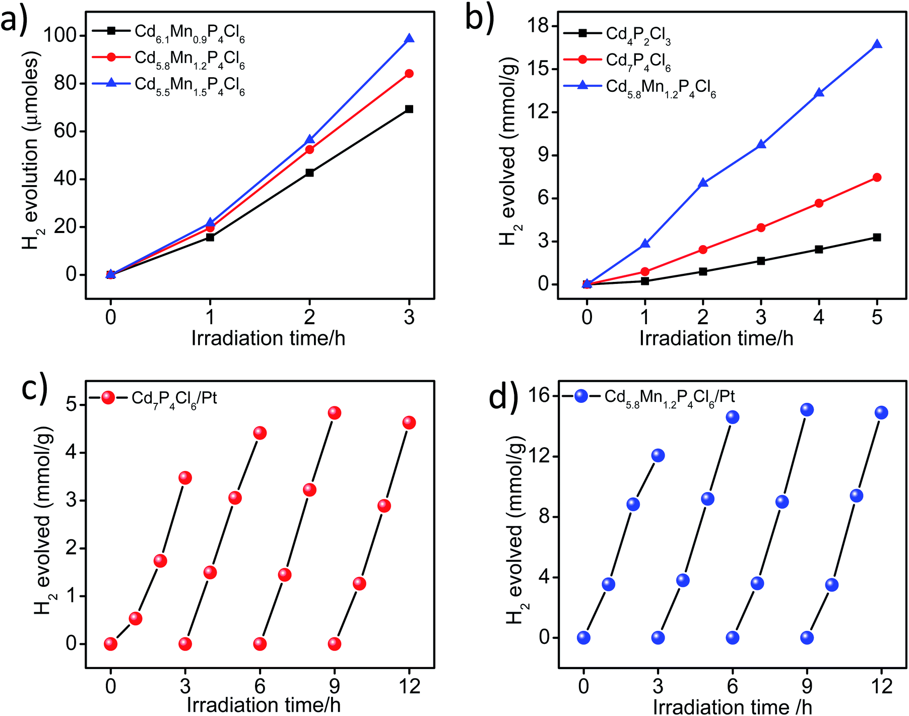
In view of the correct band edge alignments in cadmium phosphochlorides with respect to the water redox potential and their notably superior photochemical HER performance with respect to the state-of-art photocatalyst materials such as CdS and TiO2, we have examined the effect of Mn2+ substitution on the photochemical hydrogen evolution reaction properties of these compounds.1 Fig. 8a, shows visible-light-induced H2 generation from Mn2+ substituted Cd7−yMnyP4Cl6 compounds (y = 0.9 to 1.5), without any co-catalyst. All the compositions exhibit robust HER activity, an increase in the Mn2+ content enhancing the HER activity. On account of the remarkable HER performance of these photocatalysts, we have examined their activity in the presence of Pt nanocrystals (1 wt%) as a co-catalyst. In the presence of Pt nanocrystals, Cd5.8Mn1.2P4Cl6 exhibits HER activity of 9.9 mmol h−1 g−1, whereas Cd4P2Cl3 obtained at the same temperature in the absence of Mn2+ ions, exhibits the HER activity of only 1.70 mmol h−1 g−1. Cd7P4Cl6 with identical structural and absorption features as their Mn-substituted analogues (Cd7−yMnyP4Cl6) exhibits a HER activity of 4.07 mmol h−1 g−1 (Fig. 8b). Table S1† presents the comparison of HER activity of these compounds with the state-of-art semiconductor photocatalyst materials. The apparent quantum yield (AQY) of Cd5.8Mn1.2P4Cl6 is 47.6%, significantly superior to that of the pristine analogues (Cd4P2Cl3 = 8.1% and Cd7P4Cl6 = 19.5% for the AQY calculation and photon flux, please see the ESI Fig. S7†). Thus, substitution of Mn2+ in place of Cd2+ in cadmium phosphochlorides significantly enhances their photocatalytic activity. In order to further examine the stability and recyclability of these compounds, we optimized the weight of the photocatalyst (Fig. S4†) and carried out multiple HER cycles for a total duration of 12 h. Both pristine Cd7P4Cl6 and Cd5.8Mn1.2P4Cl6 exhibit an enhancement in the HER activity after the first cycle, and the activity remains consistent afterward for the entire duration of the study (Fig. 8c and d). The PXRD pattern of the pristine Cd7P4Cl6 compound obtained after the multiple cyclic studies shows broadening of peaks, indicating a loss in crystallinity due to the leaching of Cd2+ ions (Fig. S5a†), which was further confirmed by ICP-OES analysis of the reaction solution which showed released Cd2+ concentration of 0.12 ppm (after 12 h). However, the PXRD pattern of Cd5.8Mn1.2P4Cl6, do not shows any broadening of the XRD peaks, indicating its superior photostability (Fig. S5b†). Accordingly, we did not observe any detectable amount of Cd2+ in solution in the case of Cd5.8Mn1.2P4Cl6, confirming the absence of Cd2+ leaching. It is noteworthy that substitution of toxic Cd2+ ions by environment-friendly Mn2+ in Cd7−yMnyP4Cl6 gives superior photochemical HER activity and also provides better photostability.
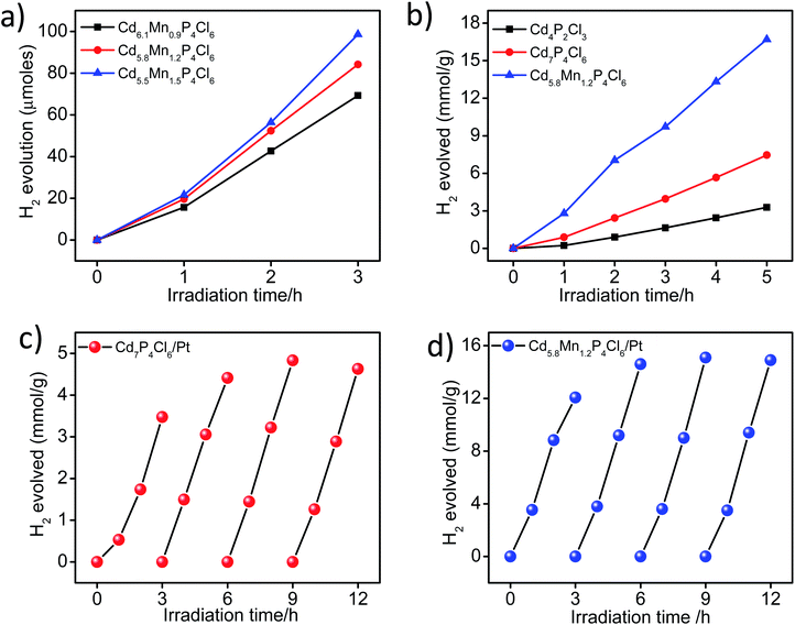 |
| | Fig. 8 Time course of H2 evolution activity of (a) bare form of Cd7−yMnyP4Cl6 compounds (b) comparative H2 evolution activity of Cd5.8Mn1.2P4Cl6, pristine Cd4P2Cl3 and Cd7P4Cl6 in the presence of 1 wt% of Pt co-catalyst, Cyclic HER activity of (c) Cd7P4Cl6 and (d) Cd5.8Mn1.2P4Cl6 in the presence of Pt co-catalyst. All the photochemical HER studied were done under visible-light irradiation in the presence of 0.18 and 0.24 M Na2S–Na2SO3 sacrificial electron donor. | |
In order to understand the enhancement in the photochemical HER activity, we have studied photogenerated charge carrier dynamics of these compounds using photoelectrochemical measurements. The open-circuit potential of the photoelectrodes demonstrates the process of charge carrier generation and recombination in materials.12,13 Pristine Cd7P4Cl6 exhibits a cathodic shift in the potential upon light irradiation, indicating n-type conductivity, similar to the earlier report (Fig. 9a).14 In contrast to the cathodic shift of the pristine compound, the manganese substituted analogue (Cd5.8Mn1.2P4Cl6) exhibits anodic shift, indicating p-type conductivity (Fig. 9b). In order to verify the nature of conduction in these compounds, Hall measurements were carried out at room temperature on the rectangular pallet of samples. Unlike the negative Hall coefficient of pristine Cd7P4Cl6 (n-type conductivity) (Fig. 9c), Cd5.8Mn1.2P4Cl6 exhibited positive Hall coefficient due to p-type conductivity (Fig. 9d). The variation of Hall voltage with the applied positive and negative magnetic field is given in ESI (Fig. S6†).
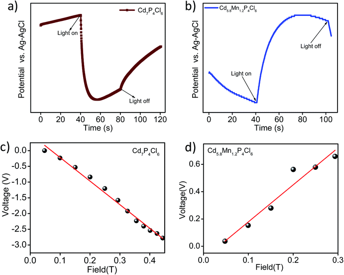 |
| | Fig. 9 Open circuit potential (OCP) of (a) pristine Cd7P4Cl6, and (b) Cd5.8Mn1.2P4Cl6. Variation of the Hall voltage with applied magnetic field in (c) Cd7P4Cl6 and (d) Cd5.8Mn1.2P4Cl6. | |
The origin of the change in conductivity upon Mn-substitution can be understood by the electronic structure of compounds (Fig. 6). The electronic states at the CBM are dominated by 3d states of Mn. Their narrow bandwidth indicates their localized nature and hence, a large effective mass and lower mobility of the electron carriers. In contrast, the states in the VBM are dominated by p-orbital of Cl and P strongly hybridized with 3d orbitals of Mn, producing notable dispersion of bands giving a low effective mass and high mobility of hole carriers. Hence, holes contribute more significantly to conduction than electrons upon Mn-substitution in these compounds causing a change in n to p-type behaviour. We note that the overall p-type conduction in Mn-substituted compounds is weaker than the n-type conduction of the pristine ones.
Since the photocatalytic activity of semiconductor materials is prone to the nature of charge carriers, we have examined the effect of the change in the type of majority carriers on the photocatalytic properties.14 It is known that when an extrinsic semiconductor comes in contact with an electrolyte bending of bands occurs at the surface to equilibrate the Fermi level.15 An n-type semiconductor with the Fermi level near CBM undergoes upward band bending in contact with the electrolyte, resulting in electron migration towards the bulk of the semiconductor and hole migration towards the interface.14 This causes a decrease in the hot electron concentration at the interface and negatively impacts the HER (Fig. 10). In contrast, a p-type semiconductor with the Fermi level close to the VBM undergoes a downward band bending in the contact of the electrolyte. Such bending of the band helps in the separation of electron and holes at the surface wherein the holes are thrown to the bulk of semiconductor and electron are pushed to the space charge region, resulting in the enrichment of photogenerated electron population in the space charge region (semiconductor–H2O interface) (Fig. 10).16 A greater population of hot electrons at the interface (space charge region) positively impacts the reduction of H2O into H2. These observations lead support to our finding that p-type Cd5.8Mn1.2P4Cl6 exhibits superior photochemical HER performance than their pristine n-type analogues.
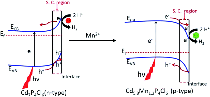 |
| | Fig. 10 Bending of bands in the pristine n-type Cd7P4Cl6 and p-type Cd5.8Mn1.2P4Cl6 showing electron depopulation (in the space charge region of Cd7P4Cl6) and electron population (in the space charge region of Cd5.8Mn1.2P4Cl6). | |
Conclusions
In summary, we find that the substitution of manganese in Cd7−yMnyP4Cl6 is more favoured than Cd4−xMnxP2Cl3, causing the former to appear at higher temperatures than the pristine material. Mn-substitution in the pristine n-type Cd7P4Cl6 transforms it into a p-type material, as exemplified by Cd5.8Mn1.2P4Cl6. Such a change in the type of conductivity remarkably influences the HER properties. Theoretical calculations indicate a significant reduction in the formation energy of Mn-substituted Cd7P4Cl6. In both the compounds, the substitutional site is more favoured than the interstitial site. The electronic structure of Cd6.75Mn0.25P4Cl6(MnCd2) does not undergo a notable change. In contrast, Cd6.75Mn0.25P4Cl6(MnCd1) and Cd3.875Mn0.125P2Cl3(MnCd1 and MnCd2) exhibit spin-split states at the VBM and CBM of the configuration in which Mn2+ is coordinated with a larger number of P atoms. Halogen vacancies are more readily introduced in Mn2+ substituted Cd7P4Cl6 when Cl vacancies are introduced at octahedrally coordinated Mn and Cd2 atoms rather than at sites localized at Mn atoms. Cl and P vacancy pairs give rise to an indirect band gap in Mn-substituted Cd7P4Cl6.
Experimental
Synthesis
In a typical synthesis, Cd3P2 (1.10 mmol), CdCl2 (1.99 mmol), red-P (0.89 mmol), and different amounts of MnCl2 were weighed inside a glove-box and ground homogenously. This homogenous precursor was transferred in a quartz tube (I. D. = 10 mm, O. D. = 12 mm) and sealed under vacuum. The sealed quartz tube was annealed at 500 °C for 24 h, followed by the cooling of the tube to room temperature with a rate of 2.5° min−1. The reaction yielded a polycrystalline powder sample of two different colors (depending on the concentration of MnCl2 taken) in the form of the lump, which was carefully separated and ground in the form of fine powder. Pristine Cd4P2Cl3 was synthesized under similar condition in the absence of MnCl2 precursor. Pristine Cd7P4Cl6 was synthesized using a homogenous mixture obtained by the grinding of stochiometric ratio of Cd-powder, red-P, and CdCl2 and annealing under sealed tube at 450 °C for 72 h.
Characterization
Powder X-ray diffraction (PXRD) patterns were recorded with a Bruker D8 Diffraction system using a Cu Kα source (λ = 0.1541 nm). UV-vis absorption spectra were collected with PerkinElmer Model Lambda 900 spectrometer. Energy dispersive spectroscopy (EDS) and elemental mapping analysis were carried out with an EDAX genesis instrument attached to the SEM instrument. X-ray photoelectron spectra (XPS) were recorded with an Omicron nanotechnology spectrometer using Al-Kα (1486.6 eV) X-ray source. Inductively coupled plasma-optical emission spectroscopy (ICP-OES) was carried out using a PerkinElmer Optima 7000 DV machine. Electron paramagnetic resonance spectra were obtained at room temperature at an operating frequency of 9.5 GHz using Bruker D8 Advance-EPR-spectrometer.
Photocatalytic H2O splitting
The photocatalytic reactions were carried out at ambient conditions using home-made cylindrical quartz cells with headspace for gas collection, closed by high-quality septa. In a typical procedure, semiconductor photocatalyst samples were dispersed in a 0.1 M NaOH aqueous solution (50 mL), and a calculated amount of H2PtCl6 solution was added (equivalent to 1 wt% of Pt). The reaction solution was purged with Ar-gas for 15–20 minutes, and UV-light was switched on for 1 h to photo-deposit the Pt nanoparticles on the semiconductor. After the photo-deposition reaction, the cell was removed from the light irradiation, and septa were taken out to add a sacrificial electron donor Na2S and Na2SO3 dissolved in 25 mL distilled water in order to make a total volume of 75 mL with Na2S and Na2SO3 concentrations of 0.18 M and 0.24 M respectively. The solution was further purged with Ar-gas for 15–20 minutes and irradiated with visible light (λ > 395 nm) using a Xe-lamp (400 W) (New-Port).
Photoelectrochemical measurements
Photoelectrochemical measurements were carried out on a CHI 1760E electrochemical work station (CH instrument Inc.) in a conventional three-electrode set-up. Spin-coated samples on FTO served as the working electrode, with a platinum wire as the counter electrode and an Ag/AgCl (saturated KCl) electrode as the reference electrode. The working electrode was prepared by spin coating. First, the catalyst slurry was prepared by ultrasonicating 20–25 mg of photocatalyst in 50 μL Nafion (5.0 wt%, Sigma Aldrich) and 250 μL of ethanol mixture. Fluorine-doped tin oxide (FTO) (2 × 1 cm2 pieces) which was used as the substrate was cleaned and dried at 100 °C. An area of 1 cm2 of the substrate was masked by scotch tape, and spin coating (750 rpm, 60 seconds) was performed on the exposed area using 15 μL of slurry each time. The electrode films were then dried under vacuum at 100 °C for 1 hour, and a Cu wire connection was made with the help of Ag-paste. The portion of the electrode, except the photocatalyst part, was electronically sealed by transparent epoxy coating and left overnight. A 0.5 M Na2SO4 aqueous solution was used as the electrolyte. A 300 W Xenon lamp, with a calibrated intensity of 100 mW cm−2 was used as the light source.
Computational methods
We have carried out first-principles calculations within density functional theory (DFT) employing VASP17,18 software package, treating the spin-dependent exchange–correlation energy with a generalized gradient approximation given by a functional parameterized by the Perdew–Burke–Ernzerhof (PBE).19 We used projected augmented wave20,21 method to describe the interaction between the valence electrons and ionic cores. Valence electron configurations used in the PAW potentials of Cd, Mn, Cl and P, are 4d10 5s2, 3d5 4s2, 3s2 3p5 and 3s2 3p3 respectively. We used a kinetic energy cut-off of 400 eV to truncate the plane wave basis for representing Kohn–Sham wave functions and a uniform mesh of 4 × 4 × 4 k-points to sample integrations over Brillouin zone (BZ). We iteratively relaxed the structures to minimize energy until Hellmann–Feynman force acting on each atom is less than 0.02 eV Å−1. Self-consistency in the Kohn–Sham solution was achieved with a convergence tolerance of 10−4 eV. In calculations of the density of states, we used electronic spectra obtained on a uniform mesh of 16 × 16 × 16 k-points in the BZ. We focus here on the structure and electronic properties of two compounds: Mn-substituted Cd7P4Cl6 and Cd4P2Cl3. We replaced one Cd-atom in the unit cell of cadmium phosphochlorides with an Mn atom to model Mn-substituted. Cadmium phosphochlorides, and simulated them with the spin-dependent DFT.
Conflicts of interest
Authors declare no conflict of interest.
Acknowledgements
A. R., thanks to the Sheikh Saqr fellowship, we thank Prof. Kanishka Biswas and Dr Tanmay Bhatt for Hall measurements and Prof. S. V. Bhat and Mr Manjunath for EPR measurements.
Notes and references
- A. Roy, A. Singh, S. A. Aravindh, S. Servottam, U. V. Waghmare and C. N. R. Rao, Angew. Chem., Int. Ed., 2019, 58, 6926–6931 CrossRef CAS PubMed.
- H. Rebbah and A. Rebbah, J. Solid State Chem., 1994, 113, 1–8 CrossRef CAS.
- A. Roy, U. S. Shenoy, K. Manjunath, P. Vishnoi, U. V. Waghmare and C. N. R. Rao, J. Phys. Chem. C, 2016, 120, 15063–15069 CrossRef CAS.
- H. Ohno, Sci, 1998, 281, 951–956 CrossRef CAS PubMed.
- Z. Li, L. Cheng, Q. Sun, Z. Zhu, M. J. Riley, M. Aljada, Z. Cheng, X. Wang, G. R. Hanson, S. Qiao, S. C. Smith and G. Q. Lu, Angew. Chem., Int. Ed., 2010, 49, 2777–2781 CrossRef CAS PubMed.
- A. Pandey and D. D. Sarma, Z. Anorg. Allg. Chem., 2016, 642, 1331–1339 CrossRef CAS.
- P. K. Santra and P. V. Kamat, J. Am. Chem. Soc., 2012, 134, 2508–2511 CrossRef CAS PubMed.
- A. Nag and D. D. Sarma, J. Phys. Chem. C, 2007, 111, 13641–13644 CrossRef CAS.
- K. Ikeue, S. Shiiba and M. Machida, Chem. Mater., 2010, 22, 743–745 CrossRef CAS.
- A. V. Shevelkov, L. N. Reshetova and B. A. Popovkin, J. Solid State Chem., 1998, 137, 138–142 CrossRef CAS.
- A. Roy, M. Chhetri, S. Prasad, U. V. Waghmare and C. N. R. Rao, ACS Appl. Mater. Interfaces, 2018, 10, 2526–2536 CrossRef CAS PubMed.
- Y. Zhang, D. Wang, X. Zhang, Y. Chen, L. Kong, P. Chen, Y. Wang, C. Wang, L. Wang and Y. Liu, Electrochim. Acta, 2016, 195, 51–58 CrossRef CAS.
- P. J. Holmes and P. Handler, J. Electrochem. Soc., 1962, 109, 228C CrossRef.
- M. Grätzel, Nature, 2001, 414, 338–344 CrossRef PubMed.
- Z. Zhang and J. T. Yates, Chem. Rev., 2012, 112, 5520–5551 CrossRef CAS PubMed.
- M. G. Kibria, F. A. Chowdhury, S. Zhao, B. AlOtaibi, M. L. Trudeau, H. Guo and Z. Mi, Nat. Commun., 2015, 6, 6797 CrossRef CAS PubMed.
- G. Kresse and J. Furthmüller, Comput. Mater. Sci., 1996, 6, 15–50 CrossRef CAS.
- G. Kresse and J. Furthmüller, Phys. Rev. B: Condens. Matter Mater. Phys., 1996, 54, 11169–11186 CrossRef CAS PubMed.
- J. P. Perdew, K. Burke and M. Ernzerhof, Phys. Rev. Lett., 1996, 77, 3865–3868 CrossRef CAS PubMed.
- P. E. Blöchl, Phys. Rev. B: Condens. Matter Mater. Phys., 1994, 50, 17953–17979 CrossRef PubMed.
- G. Kresse and D. Joubert, Phys. Rev. B: Condens. Matter Mater. Phys., 1999, 59, 1758–1775 CrossRef CAS.
Footnote |
| † Electronic supplementary information (ESI) available: EDAX and XPS spectra, UV/vis. absorption spectra, Tauc plots, PXRD of compounds before and after photochemical reactions, Hall measurement, apparent quantum yield calculations. See DOI: 10.1039/c9ra10711h |
|
| This journal is © The Royal Society of Chemistry 2020 |
Click here to see how this site uses Cookies. View our privacy policy here. 
 Open Access Article
 This Open Access Article is licensed under a Creative Commons Attribution-Non Commercial 3.0 Unported Licence
 *
*