
 Open Access Article
 This Open Access Article is licensed under a Creative Commons Attribution-Non Commercial 3.0 Unported Licence
Near-field imaging of the multi-resonant mode induced broadband tunable metamaterial absorber
Lulu Chen†
ab,
Liaoxin Sun†c,
Hongxing Dong*a,
Nanli Mouab,
Yaqiang Zhangab,
Qisong Lia,
Xiongwei Jianga and
Long Zhang *a
*a
aKey Laboratory of Materials for High-Power Laser, Shanghai Institute of Optics and Fine Mechanics, Chinese Academy of Sciences, Shanghai, 201800, China. E-mail: hongxingd@siom.ac.cn; lzhang@siom.ac.cn
bCenter of Materials Science and Optoelectronics Engineering, University of Chinese Academy of Sciences, Beijing 100049, China
cNational Laboratory for Infrared Physics, Shanghai Institute of Technical Physics, Chinese Academy of Sciences, Shanghai 200083, China
First published on 31st January 2020
Abstract
Metamaterial absorbers with tunability have broad prospects for mid-infrared absorption applications. While various methods have been proposed to control absorption, how to analyse and present the physical image of absorption mechanism in depth is still expected and meaningful. Here, we present experimental spatial near-field distributions of a multi-resonant mode induced broadband tunable metamaterial absorber by using near-field optical microscopy. The absorber is constructed by a metal double-sized unit cell and a metallic mirror separated by a thin Ge2Sb2Te5 (GST) spacer. To clearly obtain the physical images, we used a hybrid unit cell consisting of four square resonators to produce two absorption peaks at 7.8 μm and 8.3 μm. The resonance central-wavelength exhibits a redshift while switching the GST thin film from amorphous to crystalline phase. The near-field amplitude and phase optical responses of the absorber are directly observed at absorption frequencies when GST is in both phases, respectively. This work will pave the way for the fundamental science field and inspire potential applications in optical tunable absorption control.
Introduction
Metamaterial perfect absorbers (MMPAs), a kind of artificial material composed by particular structures with period unit cells in the sub-wavelength scale, have received considerable attention from extensive research studies since Landy et al. first proposed the concept.1 By virtue of their high absorbance, ultra-thin thickness and wide bandwidth merits, MMPAs in the mid-infrared spectral region are appealing to many applications in the field of diversification, such as thermal imaging,2–4 infrared camouflage,5–7 chemical sensing8,9 and radiation cooling.10,11 The near unity absorbance can be achieved by manipulating the effective permittivity and permeability of the structure simultaneously to match the free-space impedance.12 With years of continuous research, a series of metamaterial absorbers have been rapidly developed for various fields. However, the resonant frequencies of conventional MMPAs highly depend on their geometrical parameters, resulting in their resonant wavelength being single and fixed,13,14 causing restrictions for practical applications.In recent years, the development of broadband and tunable metamaterial absorbers has attracted extensive attention. By introducing functional materials including liquid crystal,15,16 graphene17–19 and phase change materials,20–24 many tunable metamaterial absorbers have been proposed to achieve dynamic modulation of absorption properties.25–30 The refractive index or conductivity of these materials can be changed by methods as diverse as optical pumping, electric current and thermal stimulus. Liquid crystals and graphene have been shown to dynamically modulate the optical properties of metamaterial absorbers, this type of material has advantages in electrical tuning. Another kind of material, like phase change materials, can undergo thermally, electrically and optically induced phase transition, which enables effective and flexible tunable absorbers to be achieved. Ge2Sb2Te5 (GST) is a representative, reversible and high-stable phase change material and has been used as a commercialized rewritable optical storage medium.31,32 The phase change of GST is a typical thermosetting process and the temperature of the phase transition from amorphous to crystalline is approximately 160 °C.33 There is an important point that the GST can remain stable below the crystalline temperature in a certain phase without thermal consumption. Moreover, there is a significant difference in the optical and electrical properties of GST between amorphous and crystalline states ranging from visible to infrared frequencies. The bistability and tremendous contrast in the refractive index between two states make GST an ideal candidate for dynamic tunable devices. Recently growing interests in GST inspire many works on tunable absorbers.24,34–39 For example, K. V. Sreekanth et al. designed and fabricated a GST-based absorber cavity with multi-narrowband perfect absorption at visible frequencies, the mechanism of tunable perfect absorption is validated using a simulation model.38 Soon after that, Li et al. experimentally demonstrated a tunable near-infrared absorber using metal–dielectric–metal structure, where GST film is selected as the middle layer.39 Although these works have made great progress, the broadband absorption structure design and absorption mechanism analyses need to be further strengthened and deepened, especially how to combine theory and experiment to analyse the physical mechanism of absorption is more important.
In this paper, we use phase-resolved scattering-type scanning near-field optical microscopy (s-SNOM) to experimentally reveal the absorption mechanism of the broadband tunable metamaterial absorber based on GST. The sandwich structure is adopted by the designed absorber, which consists of a layer of metal double-sized square resonator array and a metallic substrate separated by GST film. The hybrid unit cell is used to bring the absorption peaks at 7.8 μm and 8.3 μm closer to broaden the bandwidth. The absorptive wavelength will shift to longer wavelength after converting the GST thin film from amorphous to crystalline phase. The near-field amplitude and phase optical responses of the absorber are directly observed at absorption frequencies in two states, revealing that the resonance modes of the device at operating wavelengths have a significant difference before and after the GST phase transition. Our results will pave the way for the fundamental science field and have wide application prospect for tunable optical device field.
Results and discussion
The schematic of the designed GST-based metamaterial absorber is depicted in Fig. 1(a). The structure is based on the metal–insulator–metal (MIM) architecture, which consists of two Au layer separated by a GST film. The thickness of the top Au layer and the GST layer are fixed at 80 nm and 250 nm, and the thickness of bottom Au layer is 100 nm for blocking the transmission through the structure. There are four square resonators which have two different sizes denoted as α and β in a unit cell with period of p = 4.4 μm. The double-sized unit cell is central symmetrical, and the side length of α square w1 and β square w2 is 0.93 μm and 1 μm, respectively. The similar hybrid unit cell structure has been used to enhance the bandwidth effectively.40,41 Fig. 1(b) shows the top view of the unit cell of proposed absorber.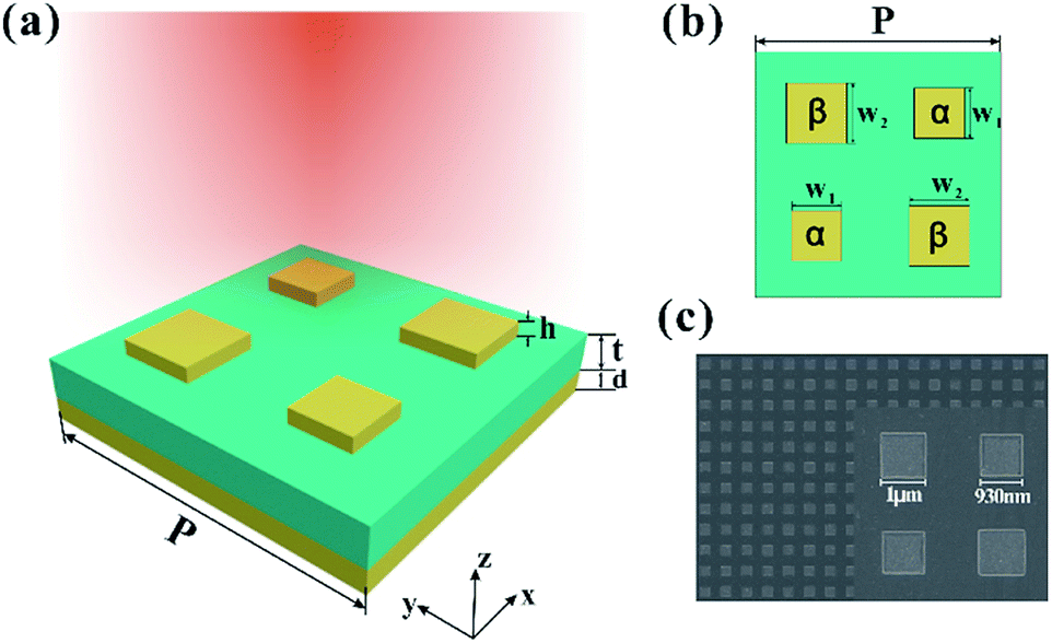 | ||
| Fig. 1 (a) Schematic of the fabricated tunable broadband metamaterial absorber incorporating phase-change material GST. The thickness of top metal square, GST spacer and bottom Au mirror are h = 80 nm, t = 250 nm and d = 100 nm, respectively. (b) Top view of the unit cell, the geometrical parameters are p = 4.4 μm, w1 = 0.93 μm, w2 = 1 μm. (c) SEM image of the fabricated sample. | ||
In order to measure the proposed absorber, an experimental sample is fabricated by the micro–nanofabrication technology. The fabrication process began with the deposition of a 100 nm-thick Au film and a 250 nm-thick GST film by magnetron sputtering methods, respectively. GST film was prepared using radio frequency sputtering from a pure Ge2Sb2Te5 (99.99%) alloy target at the pressure of 0.5 Pa by controlling Ar gas at a rate of 20 sccm. The electron beam lithography (EBL) technique was used to fabricate the pattern of square resonators. On the surface of GST film, a copolymer (MMA 8.5 MAA) layer was first spin coated and baked for 10 min at 100 °C, followed by spin-coating and baking a PMMA (polymethyl methacrylate) photoresist layer for the same operation. The purpose of PMMA/copolymer (MMA 8.5 MAA) bilayer is to obtain an undercut,42,43 which makes the lift-off easy. In our structure, the thickness of the top layer metal is 80 nm. The use of PMMA/copolymer (MMA 8.5 MAA) stack can ensure that the metal patterns are not affected by lift-off and shorten the lift-off time. For each layer, the baked temperatures are set to 100 °C to protect GST film against phase change.39 Then, the photoresist was exposed to form the square array by focused electron beam. After development, the 5 nm Cr and 75 nm Au films were deposited onto the sample surface by vacuum evaporation. The absorber is completed after a lift-off procedure in acetone. A scanning electron microscope image of the fabricated sample is presented in Fig. 1(c).
Then, the optical constants of GST film in amorphous phase (a-GST) and crystalline phase (c-GST) are measured by using spectroscopic ellipsometry (IR-VASE). A 250 nm-thick GST film was deposited on a silicon substrate, the real and imaginary parts of the complex refractive index can be obtained by model fitting the measured ellipsometry data. The GST film needs to be switched to crystalline phase because of the as-deposited GST film exhibited an amorphous phase. The phase transition is induced by annealing the GST film at 190 °C for 30 min under a nitrogen atmosphere to make sure of full crystallinity. The optical constants (n and k) of amorphous and crystalline GST samples were fitted by using a Gauss model, which are shown in Fig. 2(a). It's noteworthy that the complex refractive index in crystalline phase is quite different with the a-GST film before annealing. And the structure properties of GST films were analysed by X-ray diffraction. Fig. 2(b) shows the X-ray diffraction patterns of as-deposited and annealed GST films for 30 min at 190 °C in nitrogen atmosphere. There is no diffraction peak in the as-deposited GST film, which indicates that the film was amorphous phase. After annealed at 190 °C, peaks corresponding to (111), (200), (220), (222) planes of GST face-centered cubic structure were observed, suggesting that the GST film had crystallized into a typically fcc structure.
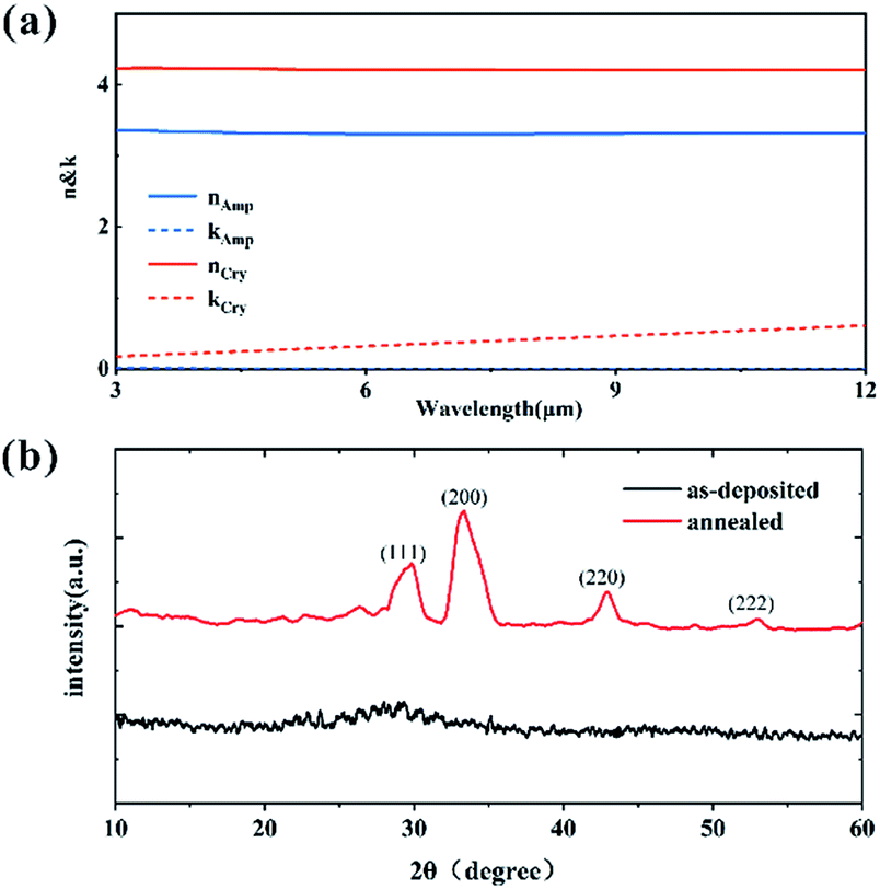 | ||
| Fig. 2 (a) Ellipsometrically measured real and imaginary parts of refractive index for GST in amorphous and crystalline phases. (b) X-ray diffractive patterns of GST films as-deposited and annealed at 190 °C. | ||
The reflection spectra of fabricated samples were measured using a Fourier-Transform Infrared (FTIR) spectrometer equipped with reflection module. The measured reflectance spectra are normalized with respect to the gold mirror. The absorption spectra were obtained by unity minus reflectance because there is no transmission in the sample. Numerical simulations of the designed structure were performed to study its absorption properties. The finite element method was used to simulate the optical response. A normal TM (or TE) polarized plane wave along −z direction was adopted to excite the structure. Periodic boundary conditions were used for a unit cell to describe equivalently an infinitely large spaces in x and y directions. The permittivity of Au was obtained from Palik's handbook.44 The optical constants of the GST film for both amorphous and crystalline phases could be obtained from abovementioned experiment.
The experimental and simulated absorption results of the sample are shown in Fig. 3(a) and (b). For comparison, the planar structure that only includes the GST film and Au film is measured to obtain the corresponding spectra. Fig. 3(a) shows that there are two peaks at 7.8 μm and 8.3 μm denoted as A peak and B peak when GST is in amorphous phase. The absorptivity of A and B peak is 0.85 and 0.88, respectively. The wavelength range in which the absorptivity exceeds 0.8 is from 7.7 μm to 8.5 μm. For simulation results, the a-GST-based absorber has two resonances peaking at 7.7 μm (with an absorptivity of 0.92) and 8.3 μm (with an absorptivity of 0.99) denoted as A1 and B1 peak, as shown in Fig. 3(b). It is noted that the measured peak absorptivity is typically lower than the simulated ones and the measured bandwidth is nearly the same. The discrepancy may be due to the imperfection of the materials in fabrication process and the error between model fitting refractive index and the actual optical constants. In contrast, for the planar sample without top resonator structures, the absorption curve is flat with the absorbance lower than 10% in the wavelength range of 6–11 μm. This comparison result indicates that the two peaks are caused by the top square resonators. We find that the two high performance absorption peaks correspond to the fundamental magnetic resonance, which arise from resonator α and β in the double-sized unit cell pattern αβαβ. The broadband absorption is due to the overlap of resonances excited by hybrid units of different sizes.
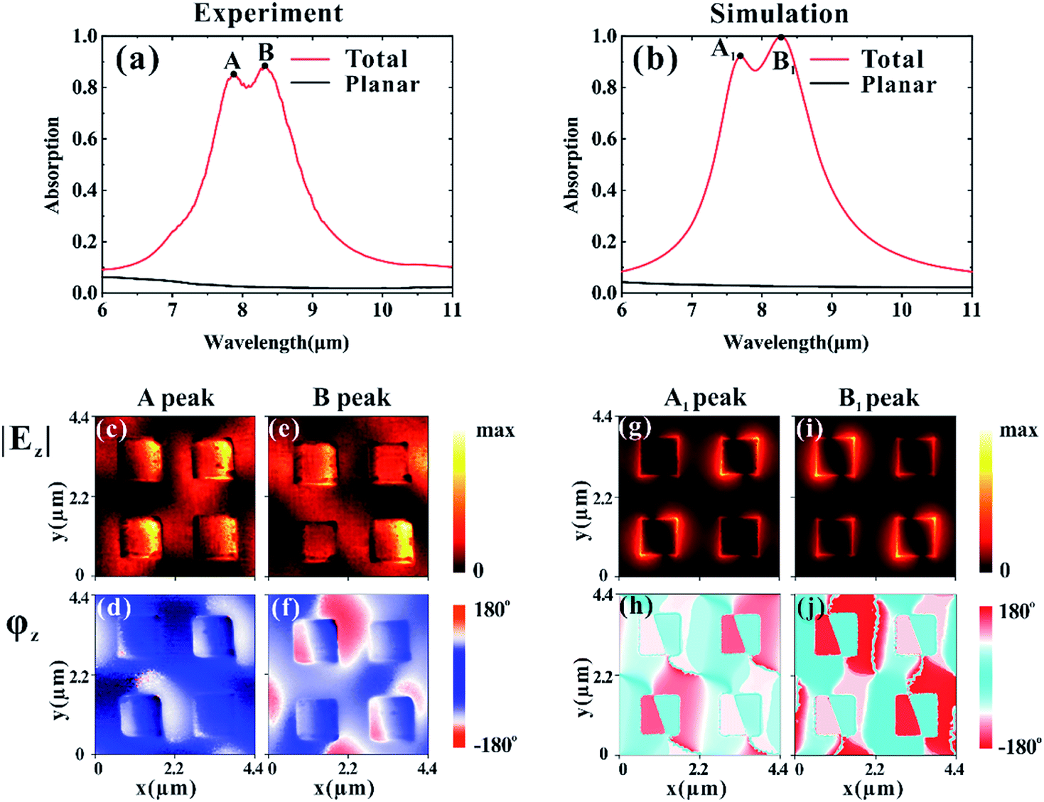 | ||
| Fig. 3 (a) Experimental and (b) simulated absorptance spectra at normal incidence for the proposed absorber and the planar sample with the amorphous GST, respectively. (c–f) Experimental and (g–j) simulated near-field amplitude |Ez| and phase φz images mapped at the spectral positions A, B, A1 and B1 marked in (a) and (b). | ||
To confirm the mechanism of broadband absorption, the s-SNOM (Neaspec GmbH) is used to measure the near-field optical properties of the metamaterial absorbers. s-SNOM is a measurement system based on the atomic force microscope (AFM), the probe tip of which is used as a source of scattering to enhance the confined electric field between the tip and the sample when a specific wavelength of light is focused on the probe. By means of heterodyne interference, probe modulation and optical path design, the near-field optical field intensity and phase image can be recorded at multiple wavelengths simultaneously. The experiments were performed when the sample was illuminated by the operating wavelength from the side at an incident angle of 60°. Fig. 3(c) and (d) display the experimental near-field amplitude |Ez| and phase φz images of vertical electric field component Ez at a fixed incident wavelength of λ = 7.8 μm. The amplitude enhanced on four resonator patterns,45 the resonator α are brighter than resonator β and the phase image exhibits a phase difference toward opposite directions at the centre of resonator α. The near-field images illuminate that the absorption mechanism of A peak is that the magnetic dipolar response at operating wavelength gives rise to the high-intensity absorption. Similarly, the near-field amplitude |Ez| and phase φz are recorded at λ = 8.3 μm (Fig. 3(e) and (f)). The remarkable changes can be observed in the experiment. It can be seen that at the operating wavelength the amplitude enhanced only on the resonator β, and the phase has a significant variation of about 180° at the centre of resonator β. The near-field images at λ = 8.3 μm are more pronounced than that at λ = 7.8 μm owing to the stronger fundamental dipolar resonance at λ = 8.3 μm. These results indicate that the multi-resonant mode excited by the hybrid unit cells result in an enhancement of absorption bandwidth. Besides, the numerical simulations for this structure have been carried out to obtain the corresponding near-field distribution (Fig. 3(g)–(j)). As seen in picture, there is very good agreement between the theoretical and the experimental results.
In Fig. 4(a) and (b), cross section of magnetic field distributions of the absorber is plotted at normal incidence. The results show the magnetic field distributions in pattern α and β of the unit cell at the wavelength of 7.7 μm and 8.3 μm, and the white arrows represent the electric-field distribution. Obviously, at the spectral positions, the top and bottom metal layers maintain the anti-parallel current, and the generated magnetic field is mainly confined in the dielectric spacer below the top Au pattern. Comparing with the magnetic field distributions at 7.7 μm and 8.3 μm, it can be seen that the resonance generated from the β pattern is stronger, and there is weak resonance caused by β pattern at 7.7 μm. This phenomenon indicates that the near-field images at the spectral position B exhibit more intuitive results.
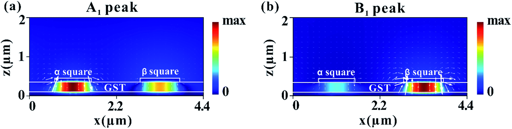 | ||
| Fig. 4 (a) and (b) are cross section view of simulated magnetic field distribution at the resonance wavelengths for a-GST sample. The color represent the intensities and the arrow represent the electric-field distribution. | ||
An important feature of the proposed absorber is that it exhibits dynamic tunability due to the phase change of ultrathin GST layer. In order to obtain flexible modulation over the absorption behaviour, the phase transition from amorphous to crystalline was induced by heating the sample above the phase transition temperature of 160 °C. Specifically, the sample undergoes an annealing process at 190 °C in a furnace under a nitrogen atmosphere for 30 min to avoid oxidation of the GST film and ensure that the GST is fully crystallized. Fig. 5(a) shows the experimental absorption curve of c-GST and a-GST absorber. For the c-GST absorber, there is only one peak with an absorptivity of 0.64 and the resonance wavelength undergo a redshift to 10.0 μm during the phase transition, which allows us to tune between two distinct mid-infrared absorption bands with a stable resonator structure. The redshift resonant features are associated with an increase in real part of the GST refractive index, and the imaginary part of the refractive index lead to the decrease of absorptivity across the spectral range presented. As a consequence, the absorption of the structure changes dramatically at certain wavelength bands. To theoretically support the experimental tunability and explore the mechanism of this phenomenon, we perform numerical simulations on the c-GST absorber. Fig. 5(b) shows the simulated absorption spectra for the total and each layer of the c-GST absorber. It can be observed that for the absorption peak of 10.0 μm, the GST layer dissipate the most of the incident energy. The magnetic field distribution at the resonance wavelength indicates that the magnetic resonance occurs on α and β patterns, simultaneously the cavity resonant mode is excited on the GST spacer (the inset of Fig. 5(b)). To reveal the intrinsic properties of the c-GST absorber, near-field optical signals of the sample was investigated using s-SNOM. Experimental and simulated near-field amplitude |Ez| and phase φz images mapped at the spectral positions C and C1 in Fig. 5(c–f). Fig. 5(c) and (d) give the measured near-field amplitude and phase images of vertical Ez component, which has the same illumination incident angle as in Fig. 3(c–f). The amplitude enhanced on four resonator patterns, and the phase has a significant variation about 180° at the centre of both resonator α and β. It means that the dipole pattern occurs on each resonator, which has a remarkable difference with the resonance of a-GST absorber. From the corresponding simulation results in Fig. 5(e) and (f), it can be seen that the simulated and experimental data are identical well.
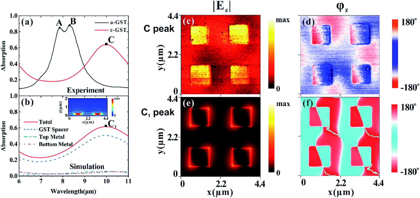 | ||
| Fig. 5 (a) Experimental absorptivity of the GST absorber between two states. The black line and red line are for the a-GST and c-GST sample. (b) The simulated spectra for the total and each layer of the c-GST absorber. Inset: the magnetic field distribution at the resonance wavelength. (c–f) Experimental and simulated near-field amplitude |Ez| and phase φz images mapped at the spectral positions C and C1. | ||
Conclusions
In summary, we have presented an active broadband tunable metamaterial absorber based on GST and used interferometric near-field scanning optical microscopy to investigate the near-field amplitude and phase optical responses at resonant frequencies. The experimental measurements show that the absorber achieves broad working band covering mid-infrared range from 7.7 μm to 8.5 μm when GST is in amorphous phase, and the absorption bands redshift after switching to the crystalline phase. And the experimental near-field optical signals of a-GST absorber provide direct evidence that such broadband absorption is owing to the multi-resonant mode excited by the hybrid unit cell. By comparing to the near-field amplitude and phase images of a-GST absorber, the resonance mode of the c-GST absorber including not only fundamental magnetic resonance but also cavity mode at operating wavelength. The results have further given the understanding of resonance modes and inspired other tunable optical devices for multifunctional integration.Conflicts of interest
There are no conflicts to declare.Acknowledgements
National Natural Science Foundation of China (NSFC) (61675219, 61875256, 61905263, 11674343, 91750103). Hongxing Dong acknowledges the Youth Top-notch Talent Support Program in Shanghai, Shanghai Rising-Star Program and Shanghai Sailing Program 18YF426300. Liaoxin Sun acknowledges Youth Innovation Promotion Association CAS (2016221).References
- N. I. Landy, S. Sajuyigbe, J. J. Mock, D. R. Smith and W. J. Padilla, Phys. Rev. Lett., 2008, 100, 207402 CrossRef CAS PubMed.
- Y. Rauste, E. Herland, H. Frelander, K. Soini, T. Kuoremaki and A. Ruokari, Int. J. Remote Sens., 2010, 18, 2641–2656 CrossRef.
- A. Tittl, A. K. Michel, M. Schaferling, X. Yin, B. Gholipour, L. Cui, M. Wuttig, T. Taubner, F. Neubrech and H. Giessen, Adv. Mater., 2015, 27, 4597–4603 CrossRef CAS PubMed.
- R. Bhargava, Appl. Spectrosc., 2012, 66, 1091–1120 CrossRef CAS PubMed.
- L. Phan, W. G. t. Walkup, D. D. Ordinario, E. Karshalev, J. M. Jocson, A. M. Burke and A. A. Gorodetsky, Adv. Mater., 2013, 25, 5621–5625 CrossRef CAS PubMed.
- C. Y. Xu, G. T. Stiubianu and A. A. Gorodetsky, Science, 2018, 359, 1495–1500 CrossRef CAS PubMed.
- O. Salihoglu, H. B. Uzlu, O. Yakar, S. Aas, O. Balci, N. Kakenov, S. Balci, S. Olcum, S. Suzer and C. Kocabas, Nano Lett., 2018, 18, 4541–4548 CrossRef CAS PubMed.
- J. Shemshad, S. M. Aminossadati and M. S. Kizil, Sens. Actuators, B, 2012, 171–172, 77–92 CrossRef CAS.
- Q. Tan, L. Tang, M. Yang, C. Xue, W. Zhang, J. Liu and J. Xiong, Optic Laser. Eng., 2015, 74, 103–108 CrossRef.
- M. M. Hossain, B. Jia and M. Gu, Adv. Opt. Mater., 2015, 3, 1047–1051 CrossRef CAS.
- C. Zou, G. Ren, M. M. Hossain, S. Nirantar, W. Withayachumnankul, T. Ahmed, M. Bhaskaran, S. Sriram, M. Gu and C. Fumeaux, Adv. Opt. Mater., 2017, 5, 1700460 CrossRef.
- E. Plum, V. A. Fedotov, P. Kuo, D. P. Tsai and N. I. Zheludev, Opt. Express, 2009, 17, 8548–8551 CrossRef CAS PubMed.
- T. Cao, C.-w. Wei, R. E. Simpson, L. Zhang and M. J. Cryan, Sci. Rep., 2014, 4, 1775–1786 CAS.
- X. Tian and Z.-Y. Li, Photonics Res., 2016, 4, 146 CrossRef CAS.
- B. Kang, J. H. Woo, E. Choi, H. H. Lee, E. S. Kim, J. Kim, T. J. Hwang, Y. S. Park, D. H. Kim and J. W. Wu, Opt. Express, 2010, 18, 16492–16498 CrossRef CAS PubMed.
- Q. Zhao, L. Kang, B. Du, B. Li, J. Zhou, H. Tang, X. Liang and B. Zhang, Appl. Phys. Lett., 2007, 90, 011112 CrossRef.
- L. Ju, B. S. Geng, J. Horng, C. Girit, M. Martin, Z. Hao, H. A. Bechtel, X. G. Liang, A. Zettl, Y. R. Shen and F. Wang, Nat. Nanotechnol., 2011, 6, 630–634 CrossRef CAS PubMed.
- T. Low and P. Avouris, ACS Nano, 2014, 8, 1086–1101 CrossRef CAS PubMed.
- Z. Y. Fang, S. Thongrattanasiri, A. Schlather, Z. Liu, L. L. Ma, Y. M. Wang, P. M. Ajayan, P. Nordlander, N. J. Halas and F. J. G. de Abajo, ACS Nano, 2013, 7, 2388–2395 CrossRef CAS PubMed.
- B. Gholipour, J. Zhang, K. F. MacDonald, D. W. Hewak and N. I. Zheludev, Adv. Mater., 2013, 25, 3050–3054 CrossRef CAS PubMed.
- W. Zhu, R. Yang, Y. Fan, Q. Fu, H. Wu, P. Zhang, N. H. Shen and F. Zhang, Nanoscale, 2018, 10, 12054–12061 RSC.
- M. A. Kats, R. Blanchard, S. Zhang, P. Genevet, C. Ko, S. Ramanathan and F. Capasso, Phys. Rev. X, 2013, 3, 041004 Search PubMed.
- K. Sun, C. A. Riedel, A. Urbani, M. Simeoni, S. Mengali, M. Zalkovskij, B. Bilenberg, C. H. de Groot and O. L. Muskens, ACS Photonics, 2018, 5, 2280–2286 CrossRef CAS.
- Y. Qu, Q. Li, K. Du, L. Cai, J. Lu and M. Qiu, Laser Photonics Rev., 2017, 11, 1700091 CrossRef.
- V. W. Brar, M. C. Sherrott, M. S. Jang, S. Kim, L. Kim, M. Choi, L. A. Sweatlock and H. A. Atwater, Nat. Commun., 2015, 6, 7032 CrossRef CAS PubMed.
- N. Mou, S. Sun, H. Dong, S. Dong, Q. He, L. Zhou and L. Zhang, Opt. Express, 2018, 26, 11728–11736 CrossRef CAS PubMed.
- D. Shrekenhamer, W. C. Chen and W. J. Padilla, Phys. Rev. Lett., 2013, 110, 177403 CrossRef PubMed.
- Z. Song, K. Wang, J. Li and Q. H. Liu, Opt. Express, 2018, 26, 7148–7154 CrossRef CAS PubMed.
- G. Zhou, P. Dai, J. Wu, B. Jin, Q. Wen, G. Zhu, Z. Shen, C. Zhang, L. Kang, W. Xu, J. Chen and P. Wu, Opt. Express, 2017, 25, 17322–17328 CrossRef CAS PubMed.
- J. K. Pradhan, S. A. Ramakrishna, B. Rajeswaran, A. M. Umarji, V. G. Achanta, A. K. Agarwal and A. Ghosh, Opt. Express, 2017, 25, 9116–9121 CrossRef CAS PubMed.
- M. Wuttig and N. Yamada, Nat. Mater., 2007, 6, 824–832 CrossRef CAS PubMed.
- Y. Hu, H. Zou, J. Zhang, J. Xue, Y. Sui, W. Wu, L. Yuan, X. Zhu, S. Song and Z. Song, Appl. Phys. Lett., 2015, 107, 263105 CrossRef.
- A. K. Michel, D. N. Chigrin, T. W. Mass, K. Schonauer, M. Salinga, M. Wuttig and T. Taubner, Nano Lett., 2013, 13, 3470–3475 CrossRef CAS PubMed.
- K. K. Du, Q. Li, Y. B. Lyu, J. C. Ding, Y. Lu, Z. Y. Cheng and M. Qiu, Light: Sci. Appl., 2017, 6, e16194 CrossRef CAS PubMed.
- Y. R. Qu, L. Cai, H. Luo, J. Lu, M. Qiu and Q. Li, Opt. Express, 2018, 26, 4279–4287 CrossRef CAS PubMed.
- Y. Meng, J. K. Behera, Y. Ke, L. Chew, Y. Wang, Y. Long and R. E. Simpson, Appl. Phys. Lett., 2018, 113, 071901 CrossRef.
- L. Zhao, X. Yang, Q. Niu, Z. He and S. Dong, Opt. Lett., 2019, 44, 3885–3888 CrossRef CAS PubMed.
- K. V. Sreekanth, S. Han and R. Singh, Adv. Mater., 2018, 30, e1706696 CrossRef PubMed.
- C. Li, W. Zhu, Z. Liu, S. Yan, R. Pan, S. Du, J. Li and C. Gu, Appl. Phys. Lett., 2018, 113, 231103 CrossRef.
- T. T. Nguyen and S. Lim, Sci. Rep., 2017, 7, 14814 CrossRef PubMed.
- A. Nagarajan, K. Vivek, M. Shah, V. G. Achanta and G. Gerini, Adv. Opt. Mater., 2018, 6, 1800253 CrossRef.
- M. C. Rosamond, J. T. Batley, G. Burnell, B. J. Hickey and E. H. Linfield, Microelectron. Eng., 2015, 143, 5–10 CrossRef CAS.
- F. Lecocq, I. M. Pop, Z. H. Peng, I. Matei, T. Crozes, T. Fournier, C. Naud, W. Guichard and O. Buisson, Nanotechnology, 2011, 22, 315302 CrossRef PubMed.
- E. D. Palik, Handbook of optical constants of solids, Academic press, 1998, vol. 3, pp. 290–295 Search PubMed.
- K. Sumar, M. Shah, A. P. Ravishankar, C. Vishwakarma, A. Dasgupta, J. Mangaonkar, G. A. Venu and U. D. Rapol, arXiv: 1810.10385, 2018.
Footnote |
| † These authors contributed equally to this work. |
| This journal is © The Royal Society of Chemistry 2020 |