
 Open Access Article
 This Open Access Article is licensed under a Creative Commons Attribution-Non Commercial 3.0 Unported Licence
A solid-state integrated photo-supercapacitor based on ZnO nanorod arrays decorated with Ag2S quantum dots as the photoanode and a PEDOT charge storage counter-electrode†
D. Solís-Cortés *a,
E. Navarrete-Astorgaa,
R. Schreblerc,
J. J. Peinado-Péreza,
F. Martína,
J. R. Ramos-Barradoa and
E. A. Dalchieleb
*a,
E. Navarrete-Astorgaa,
R. Schreblerc,
J. J. Peinado-Péreza,
F. Martína,
J. R. Ramos-Barradoa and
E. A. Dalchieleb
aUniversidad de Málaga, Andalucía Tech, Departamentos de Física Aplicada & Ingeniería Química, Laboratorio de Materiales y Superficies (Unidad Asociada al CSIC), E29071 Málaga, Spain. E-mail: dsolis@uma.es; Tel: +34 952131920
bInstituto de Física, Facultad de Ingeniería, Herrera y Reissig 565, C.C. 30, 11000 Montevideo, Uruguay
cInstituto de Química, Facultad de Ciencias, Pontificia Universidad Católica de Valparaíso, Casilla 4059, Valparaíso, Chile
First published on 6th February 2020
Abstract
A planar solid-state photocapacitor with two electrodes has been prepared for the first time using a passivated film of ZnS with Ag2S quantum dots deposited on ZnO nanorods, which were electrochemically grown on ZnO seed layers, as the photoanode. The supercapacitor part is composed of a electrodeposited poly(3,4-ethylene-dioxythiophene) PEDOT film as the counter-electrode and an ionic liquid-based electrolyte between them deposited by the dip coating method. The different nanostructures and electrodes were morphologically and structurally characterized, and the device was electrochemically characterized and could reach a potential of 0.33 V during photocharge and a storage efficiency of 6.83%.
1. Introduction
Solar photovoltaic energy conversion depends heavily on ambient factors and weather conditions (such as light intensity and day–night cycles), making the availability of solar photovoltaic power intermittent and many times unreliable.1–3 These problems impel the use of energy storage devices, which help mitigate the power output swing during generation.2–5 As solar cells of all types are unable to store the converted energy for further use, usually external energy storage devices, such as batteries and electrochemical capacitors (supercapacitors), are used in combination with solar cells.2,5–7 In recent years, due to their elevated energy efficiency, quick rechargeable capacity, long cycle life and low maintenance costs, supercapacitors have drawn growing attention among the different energy storage systems.3,5,8–12 In fact, electrochemical supercapacitors with high power density, fast charge/discharge rate (in seconds) and stable cycling performance have attained great research interest for applications in hybrid electric vehicles, portable consumer electronics and solar power plants.2,5 Moreover, the electrode materials used in supercapacitors are often cost-effective and non-toxic, making them convenient for users and environmentally friendly.2,5,6,11–13 Usually, the photoenergy converter and energy storage devices are separately operated, resulting in some space and energy consumption by the external connection system, thereby reducing the storage efficiency of the supercapacitor part.2,6,9,14,15 In order to alleviate this problem, significant efforts have been made to develop new integrated energy systems that combine the functions of both photovoltaic cells and energy storage units into a single device for high efficiency, lightweight, flexibility and portability.2,4,9,14 In this sense, devices that combine solar cells and supercapacitors for both solar energy capture and electrochemical energy storage in the same device are referred to as photo-supercapacitors or solar capacitors.3,5,15–20 For manufacturing these integrated “photocharging” energy systems, multiple solar cells technologies (e.g., dye-sensitized, organic, perovskite, and silicon) for the solar cell part and super-capacitors types (double layer, pseudo-capacitors, and hybrid) for the storage part have been combined following different approaches.3,5,7,14,16–19,21,22 At present, most of the integrated photo-supercapacitors are based on dye-sensitized solar cells and capacitors.7,15,17,18,21–23 However, to date, the integration of a quantum dot solar cell (QDSC) and a supercapacitor has hardly been reported, and the literature on this topic is scarce.3,7,15,17,18,21–23 In fact, only a couple of works dealing with photo-supercapacitors based on photoanodes made of TiO2 mesoporous layers sensitized by CdS and CdS/CdS quantum dots (QDs) are found in the literature.24,25 In this configuration, the QD-based photoanode converts solar energy into electric current, and this current is utilized to charge the supercapacitor.24,25 In this paper, a ZnO nanorod (NRs) array decorated with Ag2S QDs and one-dimensional architecture was employed as the exciton generator (the solar cell part of the photo-supercapacitor). Zinc sulphide (ZnS) was deposited over Ag2S in order to passivate the surface and avoid recombination.26 The energy band structure and physical properties of ZnO are similar to those of TiO2,27,28 whereas its electron mobility is higher (ZnO, 115–155 cm2 V−1 s−1; TiO2 10−5 cm2 V−1 s−1).27,28 Consequently, ZnO is expected to exhibit faster electron transport with less recombination loss.27,28 Furthermore, ZnO is considered as the most promising alternative to TiO2 due to its ease of crystallization and anisotropic growth.27,28 Recently, narrow bandgap semiconductor QDs, such as Ag2S, CdS, CdSe, CdTe, PbS, PbSe, InP, In2S3 and InAs, have been intensively used as sensitizers of widegap photoanodes (ZnO and TiO2 materials) in QDSCs.29–35 Among these, Ag2S is an excellent choice, particularly due to its narrow band gap (1.1 eV), which is very close to the optimal band gap value of a single junction photovoltaic device (1.13 eV), and negligible toxicity.36 On the other hand, poly(3,4-ethylene-dioxythiophene) (PEDOT), an air- and thermal-stable, environmentally benign, highly transparent and highly conductive hole conducting polymer, has been widely used as the conductive electrode in flexible electronic and optoelectronic devices.13,14,37,38 Furthermore, PEDOT exhibits a strong ability for hole transport and charge storage.13,14,39–41 Therefore, PEDOT has been used here both as a hole transport material and as a polymeric charge storage counter-electrode. Moreover, the electrolyte is another component of the photocapacitor, which plays an important role, and should have a high ionic conductivity.Recently, an interesting PVP/[HEMIm][BF4] solid-state and self-standing ion gel electrolyte was developed by our group and successfully tested on supercapacitors, (see more details in ESI†).11,16 Herein, we report for the first time, a planar photo-supercapacitor with nano-architecture composed of ZnO NR arrays decorated with Ag2S QDs as the photoelectrode (photoanode), PVP/[HEMIm][BF4] solid-state ion-gel as the electrolyte and polymeric PEDOT as the capacitor-type counter-electrode.
2. Experimental methods
2.1 Preparation of the photoelectrode
To prepare the photoelectrode part of the photocapacitor, first, ZnO nanorod arrays (NRs) (the main nanoarchitecture of the photo-storage device) were electrochemically grown onto zinc oxide thin film seed layers (SLs) deposited onto transparent substrates, which consisted of glass plates with a conductive thin film of fluorine-doped tin oxide (SnO2:F, FTO) on one side (Pilkington TEC Glass, sheet resistance of about 8 Ω □−1). The FTO/glass substrates were first cleaned by ultrasonication for 15 minutes each in acetone, 2-propanol and de-ionized water. To form the zinc oxide seed layer on each electrode, 1 mL of a Zn(CH3COO)2 (10 mM) methanolic solution was added dropwise via spin-coating (2000 rpm) for 40 seconds, and then, the sample was dried at 105 °C for 10 min. This process was repeated four times. Finally, an annealing treatment was performed under air at 350 °C for 20 min with a temperature/time ramp of 10 °C min−1. Substrates obtained following the above-described procedure were known as the one zinc oxide seed layers (1SL). Subsequently, on repeating this procedure on the prepared zinc oxide 1SL modified-FTO/glass substrate, in the second cycle, the corresponding zinc oxide 2SL FTO/glass substrates were obtained. ZnO nanorod arrays were grown from a 1 mM zinc acetate aqueous solution maintained at 70 °C by the electrochemical deposition method. As the supporting electrolyte, 0.1 M sodium acetate was employed to ensure good electrical conductivity in the aqueous solution (Milli-Q quality water, 18 MΩ cm−1). The pH of the solution was initially adjusted to 6.76. Electrodeposition was performed in a conventional three-electrode electrochemical cell with the substrate as the working electrode, a platinum sheet as the counter electrode and a saturated calomel electrode (SCE) as the reference. Electrodeposition was carried out potentiostatically at −1.0 V vs. SCE. The electrolyte was saturated with pure molecular oxygen by continuous bubbling starting 45 min prior to electrodeposition and during the growth process. The electrochemical deposition time was 3600 s. After electrodeposition, the ZnO NRs/ZnO SL/FTO/glass substrate samples were thoroughly and carefully rinsed with DI water to remove un-reacted products from the surface and dried under a moderate air flux. The ZnO NRs were selected based on the best condition determined from the experimental optimization performed previously: [ZnAc2] = 1 mM, T = 70 °C, t = 60 min.Then, the ZnO nanowire arrays were decorated with Ag2S QDs through the facile successive ionic layer adsorption and reaction (SILAR) method. The ZnO nanorod array samples were successively immersed for 1 min each in two different non-aqueous solutions, one containing Ag+ cations (50 mM AgNO3 in ethanol) and the other one containing S2− anions (50 mM Na2S in methanol). After the Ag+ and S2− dipping periods, the sample was rinsed for 40 s with ethanol (after cationic dipping) and methanol (after anionic dipping), respectively, to remove the excess ions weakly bound to the nanorod surface. This procedure completed one SILAR cycle. This Ag2S QD decoration process was repeated for 9 SILAR cycles. Then, thermal annealing was carried out at 400 °C for 1 hour in an N2 atmosphere. Finally, the ZnO NRs decorated with Ag2S QDs were passivated by the deposition of a thin ZnS layer. The passivating ZnS layer was coated onto the ZnO/Ag2S QD nanostructures using the SILAR method as well. To this end, the ZnO/Ag2S nanostructured samples were successively immersed in two different aqueous solutions for 1 min each, one containing Zn2+ cations (0.5 M of Zn(CH3COO)2) and the other containing S2− anions (0.5 M Na2S). Between each Zn2+ and S2− dipping period, the sample was rinsed with water for 40 s to remove the non-adsorbed/unreacted ions. This SILAR coating cycle was repeated 4 times. PEDOT was electrodeposited on this structure to act as the hole transporting material and as a shared electrode between the photoelectrode and the counter-electrode. Fig. 1 shows the different steps in the fabrication of the photoelectrode part of the photocapacitor.
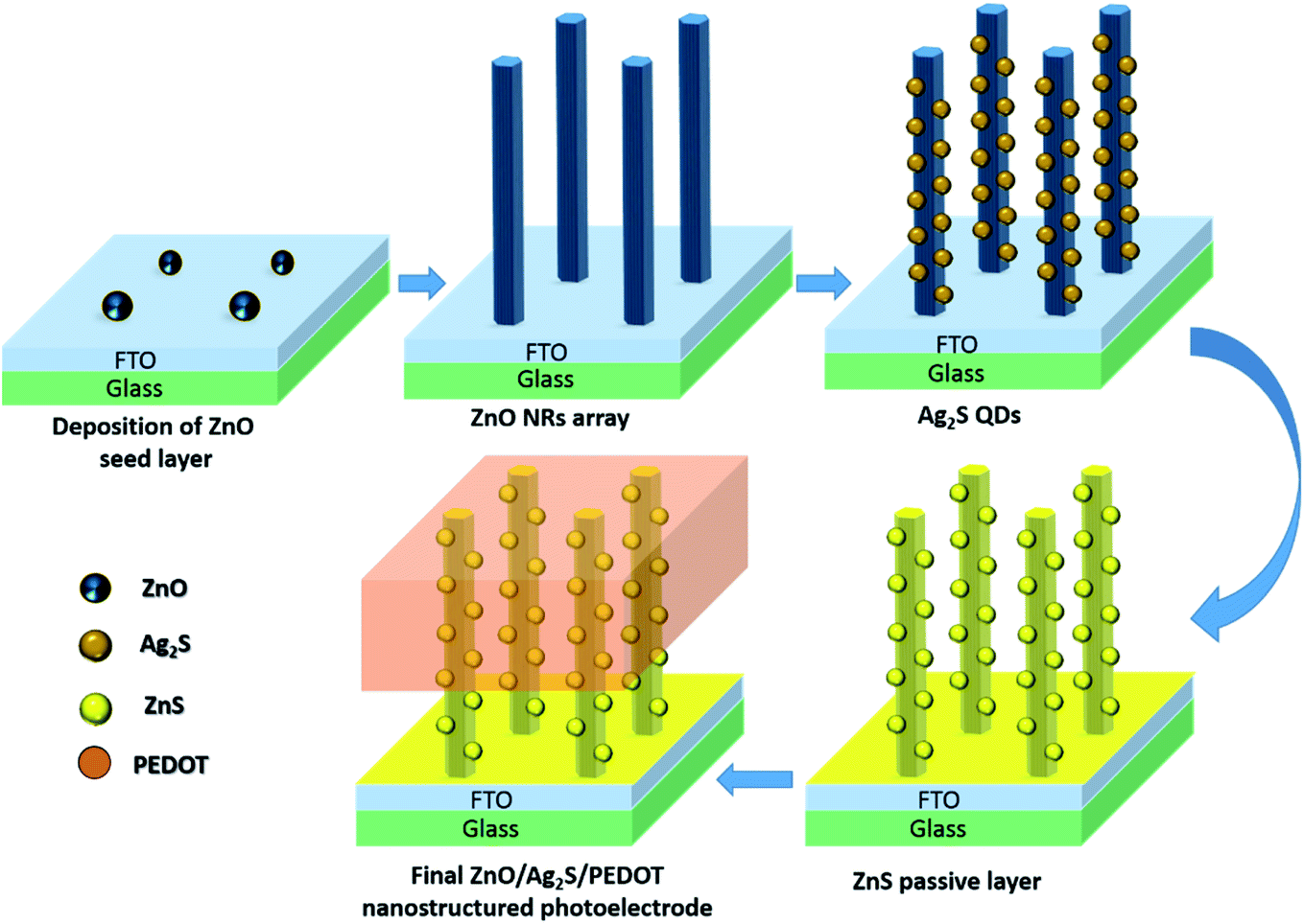 | ||
| Fig. 1 Schematic of the fabrication process of the designed nanostructured photoelectrode for the integrated photo-supercapacitor device. | ||
2.2 Supercapacitor part preparation
PEDOT was synthesized by the electropolymerization of EDOT over commercial FTO/glass substrates by employing 5 cycles of cyclic voltammetry. Once PEDOT was electrodeposited on one side of the FTO glass substrate, it was dipped in an ionic liquid solution composed of methanol, PVP and [HEMIm][BF4].2.3 Assembly of QDSSC with supercapacitor to form the integrated two-electrode photo-supercapacitor
Once the photoanode and the supercapacitor were constructed, they were assembled with a polymer separator (Solaronyx, 25 μm thickness) (size: 0.5 cm × 0.5 cm) sandwiched between the QDSSC and the counter-electrode. Both parts were connected due to the high viscosity of the electrolyte. After a while, the parts remained totally bounded, thus completing the device.2.4 Material characterization
The structural characterization of the photoelectrode was carried out by X-ray diffraction (XRD) on a PANanalytical X'Pert Pro automated diffractometer. Patterns were recorded in the Bragg–Brentano configuration using a monochromatic high intensity (Cu Kα1) radiation. An X'Celerator detector with a step size of 0.017° (2θ) was used, and the working power was 45 kV × 40 mA. The oxidation state of the chemical elements was studied via X-ray photoelectron spectroscopy (XPS) using an ESCA 5701 from Physical Electronics (PHI). An Mg Kα radiation source (15 eV) with an operating power of 400 W in an ultra-high vacuum system at a base pressure of ∼1.3 × 10⁻⁸ Pa was employed. Topographic AFM examinations were performed by using a Nanoscope V tapping-mode AFM (Veeco Instruments) employing sharp silicon tips.Field emission scanning electron microscopy (FE-SEM) images of the electrodes were obtained on a Helios Nanolab 650 Dual Beam equipment from FEI Company. High-resolution transmission electron microscopy (HRTEM) images were obtained on a Talos F200X instrument.
The electrochemical behavior of the resulting photo-supercapacitor was evaluated by cyclic voltammetry (CV), galvanostatic charge–discharge (GCD) measurements and electrochemical impedance spectroscopy (EIS) carried out at room temperature with a Biologic VSP potentiostat.
For the investigation of the photovoltaic supercapacitor performance of the photo-supercapacitor, illumination was provided by a 500 W Oriel xenon lamp with a solar filter AM1.5G, and the incident illumination power at the electrode surface was about 100 mW cm−2.
3. Results and discussion
3.1 Structural and morphological properties of the ZnS/Ag2S/ZnO photoanode
The working principle of this photocapacitor is shown in Fig. 2; the red and green arrows indicate the photo-charge and discharge processes of the supercapacitor, respectively. The mechanism was interpreted as follows: under light illumination, the Ag2S QDs are photo-excited, and the electrons from QDs are injected into the ZnO nanorods and flow through the external circuit to the counter-electrode (PEDOT), where negative charge accumulates. At the same time, the PEDOT layer electrodeposited over the ZnO nanorods of the photoanode results in a partial positive charge. The BF4− ions are attracted toward this positive charge, and the ion gel cations [HemIm]+ go to the PEDOT/FTO layer, which is the negatively charged cathode, producing the separation of the ionic liquid electrolyte and forming a double layer. The perchlorate anion (ClO4−) corresponding to the PEDOT layer suffers oxidation and reduction reactions (Fig. 5). Then, a double layer supercapacitor base is obtained. Finally, during the discharging process in darkness, the double layer reorganizes itself again. The structural and morphological characteristics of the photoanode are shown in Fig. 3. The FESEM micrograph of ZnO nanorods grown on the FTO/ZnO seed layer is shown in Fig. 3a, demonstrating a high degree of orientation along the z-axis. The top-view of the nanorods (inset) shows the characteristic hexagonal shape of the wurtzite structure. Fig. 3b shows the images of the ZnO@Ag2S core–shell NRAs. After sensitization, the NR surface became rough and grainy, which was clearly visible with spherical nanoparticles surrounding them. The morphology of the ZnO nanorods before and after QD deposition was similar, which indicated that the NR structure did not change during Ag2S QD growth. These results suggested that the Ag2S QDs were successfully deposited onto the surface of the ZnO nanorods along their entire length, forming a ZnO/Ag2S core–shell structure. Fig. 3c shows the same Ag2S@ZnO NRAs covered with ZnS, demonstrating that the film covered the entire surface of the quantum dots. It has been confirmed that this ZnS film contributes to the improvement of the photoresponse.42,43 Fig. 3d shows the tilted view of the nanostructures covered with electrodeposited PEDOT. It could be seen that PEDOT covered the surface of the nanorods, forming a uniform film.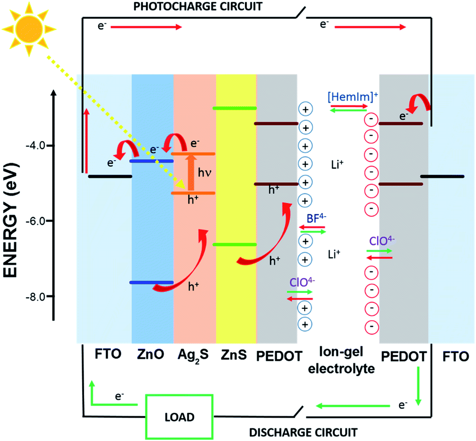 | ||
| Fig. 2 Schematic of the configuration and working mechanism of the photo-supercapacitor device. | ||
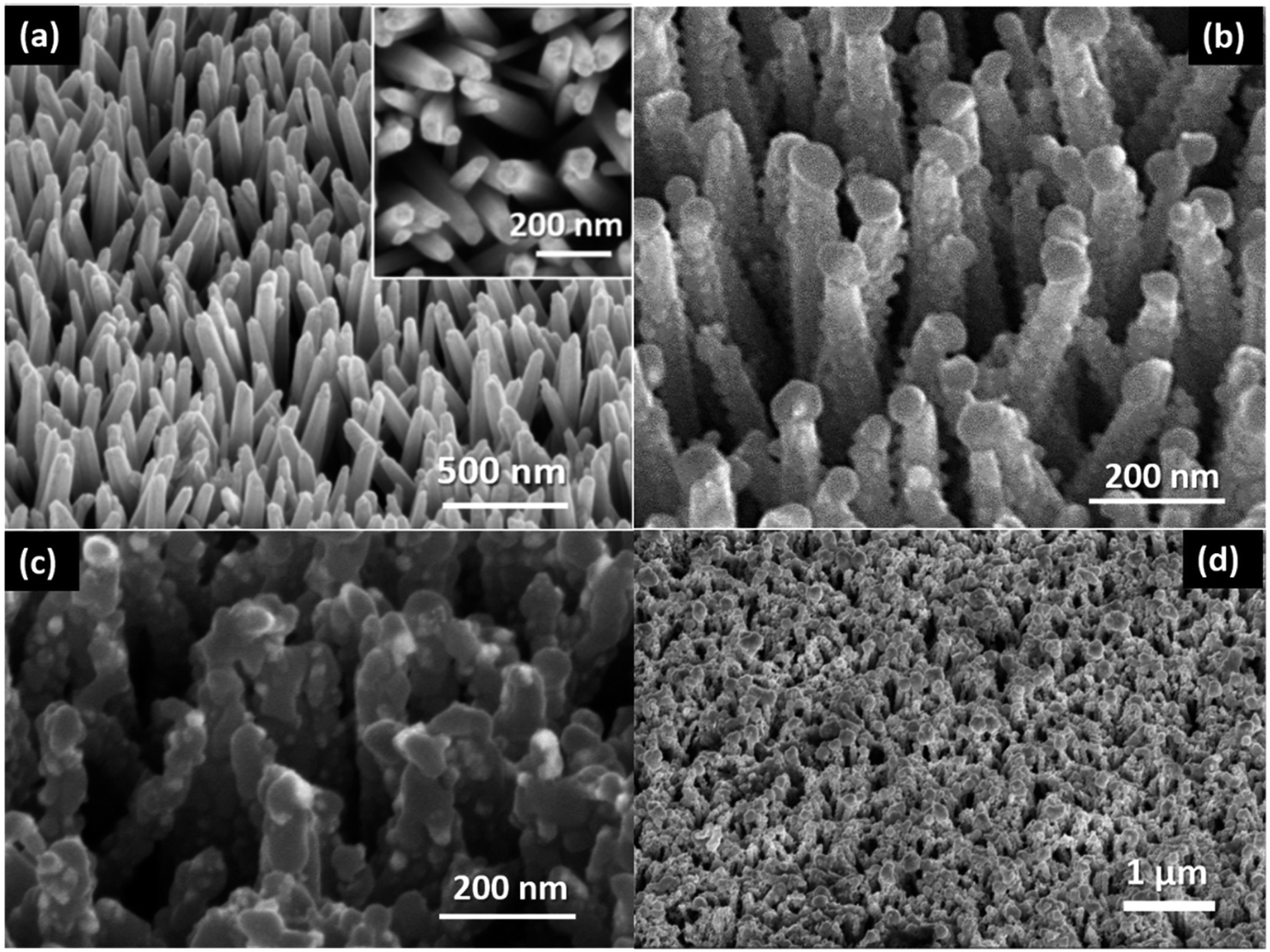 | ||
| Fig. 3 (a) Tilted FESEM micrograph of bare ZnO nanorod arrays electrochemically grown on a FTO/glass substrate. The inset of (a) shows the high magnification top view image of the ZnO nanorod arrays. (b) Tilted FESEM micrograph of the ZnO nanorod arrays after decoration with Ag2S QDs. (c) Tilted FESEM image of ZnS covering the Ag2S QDs@/ZnO NR nanostructure. (d) Tilted FESEM micrograph showing the PEDOT layer grown on the ZnS@Ag2S QDs@ZnO NR nanostructure. | ||
The finer details of the Ag2S@ZnO NRAs core–shell microstructure were further investigated by high-resolution transmission electron microscopy (HRTEM), as illustrated in Fig. 4a and b. A single Ag2S QD/ZnO NR detached from the ZnO seed layer substrate and the large number of QDs deposited onto the entire NR surface are shown (the inset displays the fast Fourier transform (FFT) image). Fig. 4b shows the magnified image of the QDs deposited on the ZnO nanorod surface. It could be observed that the Ag2S QDs had a spherical shape with a mean diameter in the range of 10–20 nm. Three lattice fringes corresponding to the monoclinic (1 1 0), (−1 1 2) and (−1 2 1) planes were marked for the nanoparticles of Ag2S, which were in accordance with the peaks in the XRD pattern (Fig. S1a, ESI†). Furthermore, the (1 1 0) and (−1 2 1) planes, which were not identified by routine XRD analysis, could be detected in this high-magnification HRTEM image.
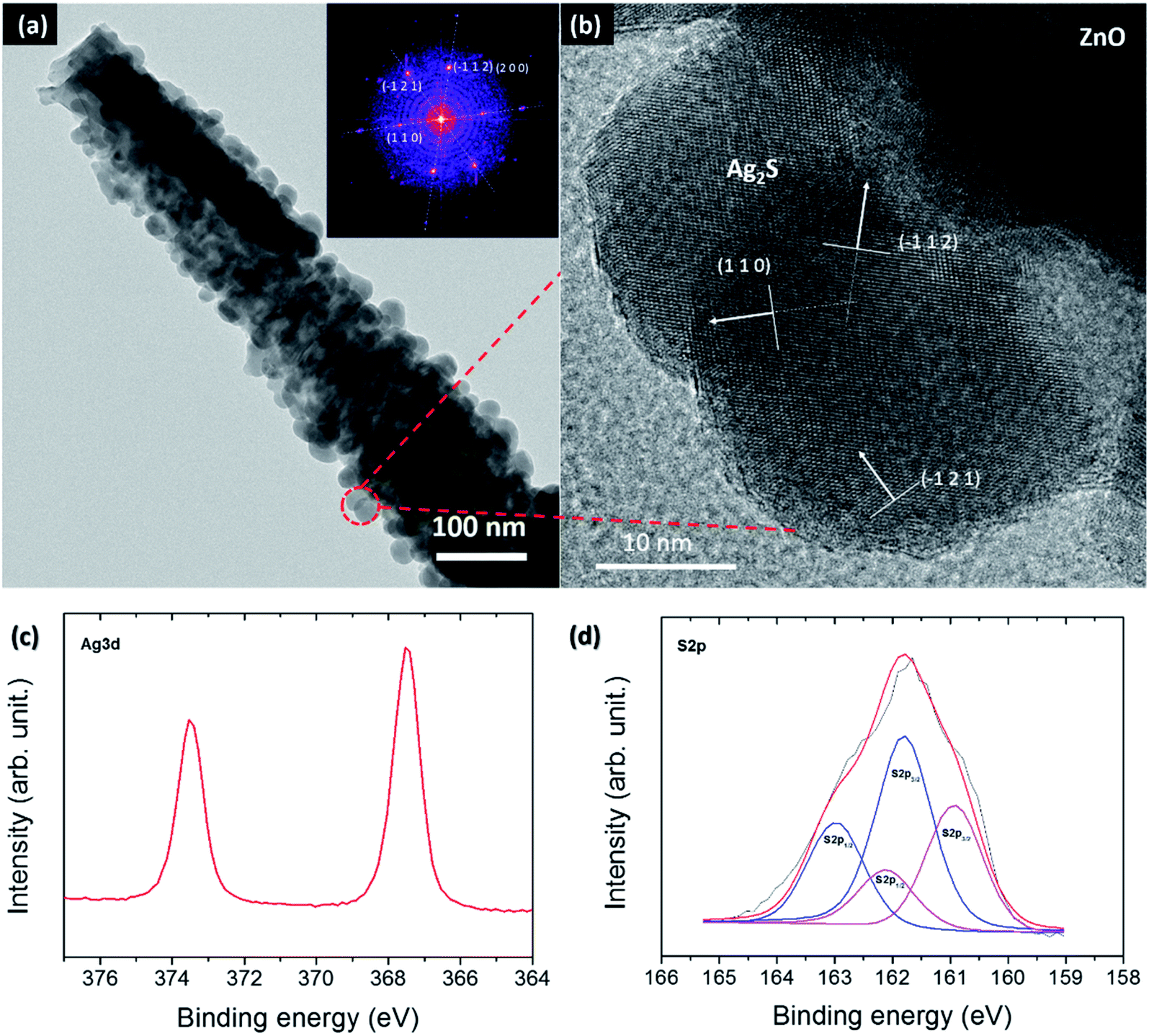 | ||
| Fig. 4 (a) HRTEM image of a single ZnO nanorod decorated with Ag2S QDs. The inset shows the FFT pattern. (b) High-magnification HRTEM image of (a) depicting individual Ag2S QDs. (c) The Ag 3d region and (d) the S 2p deconvoluted curve from XPS analysis. | ||
The C 1s, O 1s, Zn 2p, Ag 3d and S 2p core levels were measured. Fig. 4d shows the S 2p region of the XPS spectrum. The black line represents the experimental data, and the red line corresponds to the fitted curve. This peak could be deconvoluted into four peaks corresponding to S 2p3/2, S 2p1/2 in ZnS and Ag2S. The binding energy of the S 2p3/2 peak located at 161.80 eV is in accordance with the binding energy of ZnS.44–46 The lowest energy peak of S 2p3/2 was located at 160.93 eV, corresponding to Ag2S. Furthermore, the peak position of Ag 3d5/2 was located at 367.55 eV, as seen in Fig. 4c. These values are in good agreement with the reported values for Ag2S nanoparticles.46,47
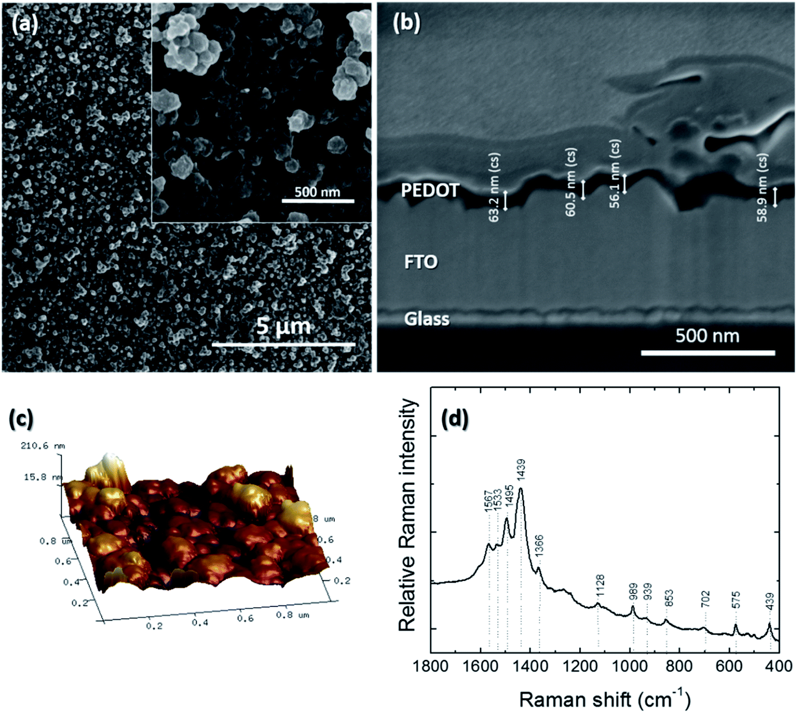
3.2 Morphological characterization of the PEDOT electrodes
Poly(3,4-ethylenedioxythiophene) (PEDOT) was electrodeposited onto FTO and exhibited a dark blue color. It was uniform with no visible defects and had good adhesion to the FTO surface. The FE-SEM micrographs of PEDOT films deposited onto FTO substrates by the potentiostatic polymerization method are presented in Fig. 5a. The low-magnification image shows a uniform and continuous film without cracks or pinholes. The inset image depicts a high-magnification image of the film, showing a dense and rough granular layer made of round-shaped particles about 200 nm in diameter. The thickness of the PEDOT film was measured from the cross-section images from field emission-scanning electron microscopy (Fig. 5b). After 5 cycles, the average thickness of the PEDOT film was 59.6 nm. Fig. 5c shows the AFM images of PEDOT over an area of 1 μm2. The roughness of the PEDOT electrodes grown for 5 cycles was 40.4 nm. In order to confirm the successful electrodeposition of the PEDOT thin film on the FTO/glass substrate, Raman spectroscopy was carried out. Fig. 5d shows the typical Raman spectrum of the PEDOT thin film in the wavenumber region 1800–400 cm−1. In Table 1, the wavenumbers of the eleven Raman peaks and comparison with studies on undoped PEDOT based on the research of Chiu et al.,63 Snyder et al.48 and Louarn et al.49 are presented. Our Raman spectrum showed a consistent match for all peaks with the corresponding Raman peaks of chemically synthesized PEDOT.50 The shift in the position of some doped PEDOT peaks relative to those of undoped PEDOT was related to the level of doping in the conducting polymer. The most intense peak was observed at 1439 cm−1, which was attributed to the Cα![[double bond, length as m-dash]](https://www.rsc.org/images/entities/char_e001.gif) Cβ (–O) symmetric stretching vibrational modes. The asymmetric CαCβ stretching modes were identified by the peaks at 1495 and 1533 cm−1. This indicated that in the electropolymerization process, PEDOT film formation involved long-chain linkage through α–β couplings. Therefore, the linkages at the β-position were formed via progressive delocalization of the unpaired electrons.51 The position of the Raman peaks corresponding to the Cβ–Cβ stretching and the Cα–Cα′ inter-ring stretching modes at 1366 and 1266 cm−1, respectively, suggested that the cation radical association also occurred by the linkage at the α–α′ (5,5′) position, which indicated short-chain PEDOT oligomers and that the molecular structure was dominantly in the trans configuration with a high regiochemical order.52 ClO4− ion conjugation during PEDOT growth was revealed by a broad peak at 939 cm−1 based on the Raman peak of free ClO4− at 934 cm−1 and that of the [Li+ClO4−] ion pairs at 948 cm−1.53 The anion (ClO4−) association in the growing chain network was caused by the positive charge in the molecular subunits of the chain, thus creating the doped state of PEDOT. Finally, from the Raman spectrum, it was concluded that conducting polymer-doped PEDOT was successfully electrodeposited onto the FTO substrates.
Cβ (–O) symmetric stretching vibrational modes. The asymmetric CαCβ stretching modes were identified by the peaks at 1495 and 1533 cm−1. This indicated that in the electropolymerization process, PEDOT film formation involved long-chain linkage through α–β couplings. Therefore, the linkages at the β-position were formed via progressive delocalization of the unpaired electrons.51 The position of the Raman peaks corresponding to the Cβ–Cβ stretching and the Cα–Cα′ inter-ring stretching modes at 1366 and 1266 cm−1, respectively, suggested that the cation radical association also occurred by the linkage at the α–α′ (5,5′) position, which indicated short-chain PEDOT oligomers and that the molecular structure was dominantly in the trans configuration with a high regiochemical order.52 ClO4− ion conjugation during PEDOT growth was revealed by a broad peak at 939 cm−1 based on the Raman peak of free ClO4− at 934 cm−1 and that of the [Li+ClO4−] ion pairs at 948 cm−1.53 The anion (ClO4−) association in the growing chain network was caused by the positive charge in the molecular subunits of the chain, thus creating the doped state of PEDOT. Finally, from the Raman spectrum, it was concluded that conducting polymer-doped PEDOT was successfully electrodeposited onto the FTO substrates.
 | ||
| Fig. 5 (a) FE-SEM top-view image of PEDOT. Inset shows the high-magnification image of the film. (b) Cross-section image of electrodeposited PEDOT on the FTO substrate. (c) AFM image and (d) Raman spectrum (532 nm excitation) of electrochemically prepared PEDOT. | ||
| Excitation wavelength | Approximate description of vibrational modes | ||
|---|---|---|---|
| 532 nm (cm−1) doped PEDOT (this work) | 785 nm (cm−1)63 undoped PEDOT | 1064 nm (cm−1)48,49 undoped PEDOT | |
| 1533 | 1516 | 1520 | Asymmetric CαCβ stretching |
| 1439 | 1414 | 1431 | Symmetric CαCβ (–O) stretching |
| 1366 | 1370 | 1369 | Cβ–Cβ stretching |
| 1266 | 1252 | 1226/1270 | Cα–Cα′ (inter-ring) stretching |
| 1128 | 1097 | 1111 | C–O–C deformation |
| 989 | 990 | 991 | Oxyethylene ring deformation |
| 702 | 699 | 692 | Symmetric C–S–C deformation |
| 575 | 578 | 571 | Oxyethylene ring deformation |
3.3 Electrochemical performance
Fig. 6a shows the cyclic voltammograms obtained at different scan rates (50, 100, 150 and 200 mV s−1) with higher areas under the curves at higher scan rates, as expected. The shape of the curves was almost rectangular at all scan rates, indicating low resistance and good reversibility. As shown in Fig. 6b, the near-triangular shape of the galvanostatic charge–discharge curves at different current densities indicated the quasi-reversible process characteristic of the pseudocapacitor. To analyze the cyclic stability of the photocapacitor, the specific capacitance and specific energy were calculated from the CV curves obtained from 1200 cycles (Fig. 6c), and the resulting values are plotted in Fig. 6d. Specific capacitances from 0.334 mF cm−2 to 0.339 mF cm−2 were achieved under dark conditions depending on the voltammetry cycle number. Furthermore, specific energies from 7.44 μJ cm−2 to 7.53 μJ cm−2 were obtained. Though both values decreased with the cycle number, this decrease was not very relevant considering the number of cycles (1200).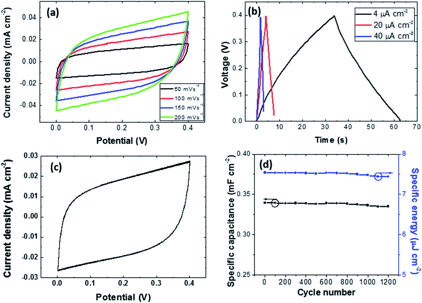 | ||
| Fig. 6 (a) Cyclic voltammetry curves at different scan rates in darkness. (b) Galvanostatic charge–discharge curves at different current densities. (c) Cyclic voltammograms measured at 100 mV s−1 from 1200 cycles. (d) Specific capacitance (black circles) and specific energy (blue circles) values obtained from the CV curves of the photocapacitor. | ||
3.4 Impedance analysis
In order to study the photocapacitor device characteristics, electrochemical impedance spectroscopy (EIS) measurements were recorded at four different applied bias potentials E = 0.0 V, 0.1 V, 0.2 V and 0.3 V under dark conditions. The obtained values are depicted in Table 2. Fig. 7a and b show the typical Nyquist and Bode plots of the photocapacitor device under study at the applied bias potential E = 0.0 V. The fits indicated by solid lines in the plots showed good agreement with the data. This confirmed the suitability of the equivalent circuit model used. The Nyquist plot consisted of an incomplete small semicircle at the higher frequency region with a non-zero intercept and a linear tail at lower frequencies. The impedance at high frequencies showed low resistive behaviour with the series resistance of 136.2 Ω at 0.0 V, which remained constant at higher applied voltages. Series resistance (Rs) represents the sheet resistance of FTO and the contact resistance of the FTO/ZnO nanorods. The semicircle with a linear tail in the Nyquist plot suggested that the polarization was due to a combination of diffusion and kinetic processes. Parallel resistance (Rp) represents the resistance to leakage currents in the photocapacitor, and their values were very high and increased with applied voltage. These results meant a low leakage current and therefore very low electronic conductivity in the PVP/[HEMIm][BF4] electrolyte. The capacitor could be equivalent to a constant phase element (CPE and Q, in this case) because both electrodes do not have a double-layer behaviour, this indicates that the supercapacitor do not correspond to an ideal capacitor.| Applied bias potential (V) | ||||
|---|---|---|---|---|
| 0 | 0.1 | 0.2 | 0.3 | |
| Rs (Ω) | 136.2 | 157.1 | 155.7 | 154.2 |
| CPE (S sα) | 6.06 × 10⁻⁶ | 7.5 × 10⁻⁶ | 9.5 × 10⁻⁶ | 1.24 × 10⁻⁵ |
| α | 0.682 | 0.669 | 0.649 | 0.628 |
| Rp (MΩ) | 0.979 | 1.67 | 2.33 | 7.70 |
| Rct (Ω) | 1063 | 1582 | 1856 | 2072 |
| Q (S sn) | 8.74 × 10⁻⁶ | 6.52 × 10⁻⁶ | 6.70 × 10⁻⁶ | 7.46 × 10⁻⁶ |
| n | 0.835 | 0.826 | 0.832 | 0.844 |
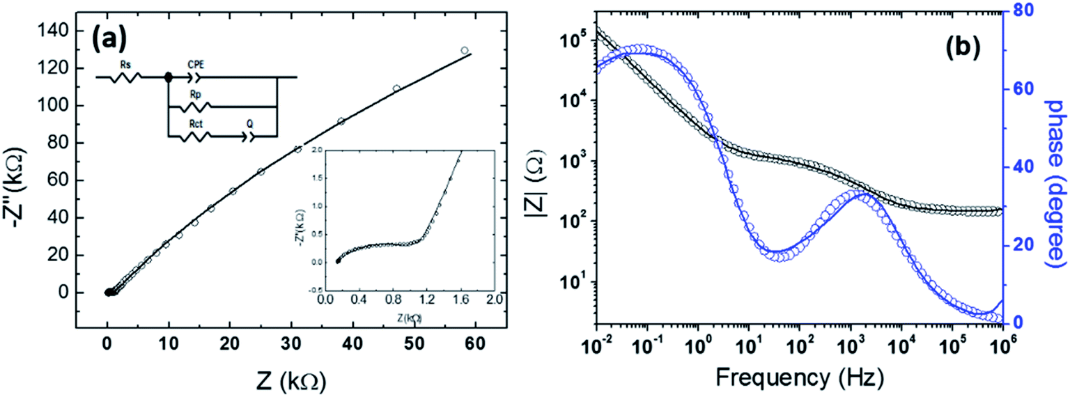 | ||
| Fig. 7 (a) Nyquist and (b) Bode plots recorded for the photocapacitor device at an applied bias potential of 0.0 V under dark conditions. The symbols (open circle shapes) stand for experimental data; the solid lines are the curves fitted to the electrical circuit model depicted in the inset of (a). The inset shows the high frequency region. | ||
The “n” values were nearly 1, which indicated that this QPE approached the capacitance of a rough surface of 40.4 nm, which was confirmed by the AFM characterization of the PEDOT electrodes (Fig. 4c). The values obtained for Rct were not very high and indicated an electron transfer reaction in the photoanode.
3.5 Photovoltaic supercapacitor performance
Fig. 8a shows the photocharge and galvanostatic discharge process (in dark) of the photosupercapacitor at different discharge current densities from 4 to 400 μA cm−2. The device was totally photocharged to a final work potential of 0.33 V in 40 s and the process was maintained for 600 s consistently. The voltage achieved is higher than those of other photocapacitors composed of two electrodes54,55 and even with three electrodes reported in the literature.56 The photocharge time was lower than that reported in another study,57 which was higher than 2000 s. After photocharge, the device was discharged at 4 μA cm−2 in a discharge time of 55 s, at 40 μA cm−2 in 2 s and at 400 μA cm−2 in 1 s. As expected, the discharge time decreased with the applied current density, achieving 100 s for the lowest value of current density. This discharge time was comparable to those of other photocapacitors with higher applied discharge current density.4,58 Some cycles of photocharge and galvanostatic discharge (in dark) carried out at 4 μA cm−2 are presented in Fig. 8b, showing the stability of the photocapacitor through the cycling process (50 cycles). The performance of the integrated photocapacitor was evaluated by calculating the ηoverall and ηstorage values from the photocharge–discharge curves. The capacitance of the device was 0.667 mF cm−2, which is higher than that reported in another work that employed ZnO as the photoelectrode and graphene as the counter-electrode59 and in the range of another photosupercapacitor based on Bi-polar TiO2 nanotubes.60 The calculated stored energy was reached the value of 3.63 × 10⁻⁵ W h cm−2. Furthermore, the integrated photocapacitor reached the maximum overall photoelectric efficiency of ηoverall = 8.25 × 10⁻⁴% and maximum storage efficiency of ηstorage = 6.83%. Although other photocapacitors with higher efficiencies exist in the literature,61,62 the concept of photocapacitor is promising and the device exhibits good capacitance, less photo-charge time and stability in repeated photocharge–discharge cycles. Furthermore, this two-electrode device is low in cost, environmentally friendly and easy to fabricate.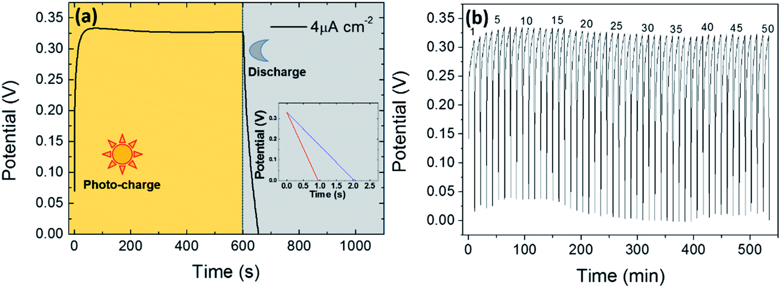 | ||
| Fig. 8 (a) Photocharge under AM1.5G simulated sunlight (100 mW cm−2) illumination and galvanostatic discharge at 4 μA cm−2 in dark conditions (inset shows the galvanostatic discharge at 40 μA cm−2 (blue line) and 400 μA cm−2 (red line) current densities). (b) Some cycles of photocharge/galvanostatic discharge at 4 μA cm−2. Cycle numbers are indicated. | ||
4. Conclusions
In conclusion, a two-electrode solid-state integrated photo-supercapacitor containing ZnO nanorod arrays decorated with Ag2S quantum dots as the photoanode, a PEDOT charge storage counter-electrode and an ion-gel electrolyte was successfully obtained. The FE-SEM images of the photoanode showed the electrochemical growth of the ZnO nanorod arrays with a high degree of orientation along the z-axis. The HRTEM image of the Ag2S quantum dots demonstrated that they covered the entire nanorod surface and had an average diameter of 10–20 nm. The presence of ZnS over Ag2S was identified through XPS analysis. A symmetric supercapacitor based on PEDOT electrodes and PVP/[HEMIm][BF4] electrolyte was developed as the charge storage part of the photo-supercapacitor. Its specific capacitance was 0.667 mF cm−2, and the storage efficiency was 6.83%. The photosupercapacitor showed high stability with the photocharge and discharge cycles achieving a maximum voltage of 0.33 V in 40 s.This configuration of the two-electrode photocapacitor offers an interesting starting point to improve the efficiency and reduce the cost of three-electrode photocapacitor production without employing dyes as sensitizers.
Conflicts of interest
There are no conflicts of interest to declare.Acknowledgements
This work was supported by projects RNM1399 and TEC 2014-53906-R, Junta de Andalucía and Ministry of Science and Universities of Spain respectively. E. A. D. acknowledges CSIC (Comisión Sectorial de Investigación Científica), Universidad de la República, Montevideo, Uruguay, PEDECIBA – Física. R. S. is grateful to DII of PUCV and FONDECYT Grant No. 1160485, Chile.References
- M. R. Lukatskaya, B. Dunn and Y. Gogotsi, Nat. Commun., 2016, 7, 1–13 CrossRef PubMed.
- J. Liang, G. Zhu, Z. Lu, P. Zhao, C. Wang, Y. Ma, Z. Xu, Y. Wang, Y. Hu, L. Ma, T. Chen, Z. Tie, J. Liu and Z. Jin, J. Mater. Chem. A, 2018, 6, 2047–2052 RSC.
- V. Vega-Garita, L. Ramirez-Elizondo, N. Narayan and P. Bauer, Prog. Photovoltaics Res. Appl., 2019, 27, 346–370 CrossRef.
- J. Xu, Z. Ku, Y. Zhang, D. Chao and H. J. Fan, Adv. Mater. Technol., 2016, 1, 1–5 Search PubMed.
- P. Simon and Y. Gogotsi, Nat. Mater., 2008, 7, 845–854 CrossRef CAS PubMed.
- N. Bagheri, A. Aghaei, M. Y. Ghotbi, E. Marzbanrad, N. Vlachopoulos, L. Häggman, M. Wang, G. Boschloo, A. Hagfeldt, M. Skunik-Nuckowska and P. J. Kulesza, Electrochim. Acta, 2014, 143, 390–397 CrossRef CAS.
- D. Schmidt, M. D. Hager and U. S. Schubert, Adv. Energy Mater., 2016, 6, 1500369 CrossRef.
- X. Xia, J. Luo, Z. Zeng, C. Guan, Y. Zhang, J. Tu, H. Zhang and H. J. Fan, Sci. Rep., 2012, 2, 981 CrossRef PubMed.
- J. Xu, H. Wu, L. Lu, S. F. Leung, D. Chen, X. Chen, Z. Fan, G. Shen and D. Li, Adv. Funct. Mater., 2014, 24, 1840–1846 CrossRef CAS.
- J. Rodríguez-Moreno, E. Navarrete-Astorga, E. A. Dalchiele, R. Schrebler, J. R. Ramos-Barrado and F. Martín, Chem. Commun., 2014, 50, 5652–5655 RSC.
- E. Navarrete-Astorga, J. Rodríguez-Moreno, E. A. Dalchiele, R. Schrebler, P. Leyton, J. R. Ramos-Barrado and F. Martín, J. Solid State Electrochem., 2017, 21, 1431–1444 CrossRef CAS.
- J. Rodríguez-Moreno, E. Navarrete-Astorga, E. A. Dalchiele, L. Sánchez, J. R. Ramos-Barrado and F. Martín, J. Power Sources, 2013, 237, 270–276 CrossRef.
- J. Rodríguez-Moreno, E. Navarrete-Astorga, E. A. Dalchiele, R. Schrebler, J. R. Ramos-Barrado and F. Martín, Chem. Commun., 2014, 5652, 5652–5655 RSC.
- Y. Jin, Z. Li, L. Qin, X. Liu, L. Mao, Y. Wang, F. Qin, Y. Liu, Y. Zhou and F. Zhang, Adv. Mater. Interfaces, 2017, 4, 1–8 Search PubMed.
- Y. Sun and X. Yan, Sol. RRL, 2017, 1, 1700002 CrossRef.
- E. Navarrete-Astorga, D. Solís-Cortés, J. Rodríguez-Moreno, E. A. Dalchiele, R. Schrebler, F. Martín and J. R. Ramos-Barrado, Chem. Commun., 2018, 54, 10762–10765 RSC.
- R. Liu, Y. Liu, H. Zou, T. Song and B. Sun, Nano Res., 2017, 10, 1545–1559 CrossRef CAS.
- M. Yu, W. D. McCulloch, Z. Huang, B. B. Trang, J. Lu, K. Amine and Y. Wu, J. Mater. Chem. A, 2016, 4, 2766–2782 RSC.
- N. Vlachopoulos and A. Hagfeldt, in Molecular Devices for Solar Energy Conversion and Storage, Springer Nature, 2018 Search PubMed.
- T. Song and B. Sun, ChemSusChem, 2013, 6, 408–410 CrossRef CAS PubMed.
- T. R. Cook, D. K. Dogutan, S. Y. Reece, Y. Surendranath, T. S. Teets and D. G. Nocera, Chem. Rev., 2010, 110, 6474–6502 CrossRef CAS PubMed.
- B. Luo, D. Ye and L. Wang, Adv. Sci., 2017, 4, 1–15 Search PubMed.
- J. Xu, Y. Chen and L. Dai, Nat. Commun., 2015, 6, 1–7 Search PubMed.
- R. Narayanan, P. N. Kumar, M. Deepa and A. K. Srivastava, Electrochim. Acta, 2015, 178, 113–126 CrossRef CAS.
- C. Shi, H. Dong, R. Zhu, H. Li, Y. Sun, D. Xu, Q. Zhao and D. Yu, Nano Energy, 2015, 13, 670–678 CrossRef CAS.
- N. Guijarro, J. M. Campiña, Q. Shen, T. Toyoda, T. Lana-Villarreal, R. Gómez and R. Go, Phys. Chem. Chem. Phys., 2011, 13, 12024–12032 RSC.
- G. Guerguerian, F. Elhordoy, C. J. Pereyra, R. E. Marotti, F. Martín, D. Leinen, J. R. Ramos-Barrado and E. A. Dalchiele, Nanotechnology, 2011, 22, 505401 CrossRef PubMed.
- L. Campo, C. J. Pereyra, L. Amy, F. Elhordoy, R. E. Marotti, F. Martin, J. R. Ramos-Barrado, E. a. Dalchiele, F. Mart, F. Martín, J. R. Ramos-Barrado and E. a. Dalchiele, ECS J. Solid State Sci. Technol., 2013, 2, Q151–Q158 CrossRef CAS.
- P. V. Kamat, Acc. Chem. Res., 2012, 45, 1906–1915 CrossRef CAS PubMed.
- C. Chen, Y. Xie, G. Ali, S. H. Yoo and S. O. Cho, Nanotechnology, 2010, 22, 15202 CrossRef PubMed.
- Y. Chen, L. Wei, G. Zhang and J. Jiao, Nanoscale Res. Lett., 2012, 7, 1–6 CrossRef CAS PubMed.
- M. Shalom, S. Buhbut, S. Tirosh and A. Zaban, J. Phys. Chem. Lett., 2012, 3, 2436–2441 CrossRef CAS PubMed.
- J. Joo, D. Kim, D. J. Yun, H. Jun, S. W. Rhee, J. Sung Lee, K. Yong, S. Kim and S. Jeon, Nanotechnology, 2010, 21, 325604 CrossRef PubMed.
- H. Wang, T. Wang, X. Wang, R. Liu, B. Wang, H. Wang, Y. Xu, J. Zhang and J. Duan, J. Mater. Chem., 2012, 22, 12532–12537 RSC.
- S. H. Im, H. J. Kim, S. Kim, S. W. Kim and S. Il Seok, Org. Electron., 2012, 13, 2352–2357 CrossRef CAS.
- H. Shen, X. Jiao, D. Oron, J. Li and H. Lin, J. Power Sources, 2013, 240, 8–13 CrossRef CAS.
- M. M. Islam, A. T. Chidembo, S. H. Aboutalebi, D. Cardillo, H. K. Liu, K. Konstantinov and S. X. Dou, Front. Energy Res., 2014, 2, 1–11 CAS.
- S. Dhar, T. Majumder, P. Chakraborty and S. P. Mondal, Org. Electron., 2018, 53, 101–110 CrossRef CAS.
- Y. Wang, P. Shao, Q. Chen, Y. Li, J. Li and D. He, J. Phys. D: Appl. Phys., 2017, 50, 175105 CrossRef.
- B. Babakhani and D. G. Ivey, Electrochim. Acta, 2010, 55, 4014–4024 CrossRef CAS.
- J. Rodríguez-Moreno, E. Navarrete-Astorga, F. Martín, R. Schrebler, J. R. Ramos-Barrado and E. A. Dalchiele, Thin Solid Films, 2012, 525, 88–92 CrossRef.
- V. González-Pedro, X. Xu, I. Mora-Seró and J. Bisquert, ACS Nano, 2010, 4, 5783–5790 CrossRef.
- M. Wang, C. Chen, H. Qin, L. Zhang, Y. Fang, J. Liu and L. Meng, Adv. Mater. Interfaces, 2015, 2, 1–10 Search PubMed.
- T. Vdovenkova, A. Vdovenkov and R. Tornqvist, Thin Solid Films, 1999, 343–344, 332–334 CrossRef.
- D. Lin, H. Wu, R. Zhang, W. Zhang and W. Panw, J. Am. Ceram. Soc., 2010, 93, 3384–3389 CrossRef CAS.
- D. Briggs, C. D. Wanger, W. M. Riggs, L. E. Davis, J. F. Moulder and G. E. Muilenberg, Handbook of X-ray photoelectron spectroscopy: a reference book of standard data for use in X-ray photoelectron spectroscopy, PerkinElmer Corp., 1979 Search PubMed.
- W. Zhang, L. Zhang, Z. Hui, X. Zhang and Y. Qian, Solid State Ionics, 2000, 130, 111–114 CrossRef CAS.
- R. G. Snyder and G. Zerbi, Spectrochim. Acta A, 1967, 23, 391–437 CrossRef.
- G. Louarn, J. P. Buisson, S. Lefrant and D. Fichou, J. Phys. Chem., 1995, 99, 11399–11404 CrossRef CAS.
- S. Garreau, G. Louarn, J. P. Buisson, G. Froyer and S. Lefrant, Macromolecules, 1999, 32, 6807–6812 CrossRef CAS.
- P. Pfluger and G. B. Street, J. Chem. Phys., 1984, 80, 544–553 CrossRef CAS.
- D. H. Han, J. W. Kim and S. M. Park, J. Phys. Chem. B, 2006, 110, 14874–14880 CrossRef CAS PubMed.
- J. S. Loring and W. Ronald Fawcett, J. Phys. Chem. A, 1999, 103, 3608–3617 CrossRef CAS.
- X. Zhang, X. Huang, C. Li and H. Jiang, Adv. Mater., 2013, 25, 4093–4096 CrossRef CAS PubMed.
- P. J. Kulesza, M. Skunik-Nuckowska, K. Grzejszczyk, N. Vlachopoulos, L. Yang, L. Haggman and A. Hagfeldt, ECS Trans., 2013, 50, 235–244 CrossRef.
- P. A. Mini, S. V. Nair and K. R. V. Subramanian, Prog. Photovoltaics Res. Appl., 2012, 21, 1153–1157 Search PubMed.
- A. Takshi, H. Yaghoubi, T. Tevi and S. Bakhshi, J. Power Sources, 2015, 275, 621–626 CrossRef CAS.
- S. C. Lau, H. N. Lim, T. B. S. A. Ravoof, M. H. Yaacob, D. M. Grant, R. C. I. MacKenzie, I. Harrison and N. M. Huang, Electrochim. Acta, 2017, 238, 178–184 CrossRef CAS.
- J. Bae, Y. J. Park, M. Lee, S. N. Cha, Y. J. Choi, C. S. Lee, J. M. Kim and Z. L. Wang, Adv. Mater., 2011, 23, 3446–3449 CrossRef CAS PubMed.
- J. Xu, H. Wu, L. Lu, S. F. Leung, D. Chen, X. Chen, Z. Fan, G. Shen and D. Li, Adv. Funct. Mater., 2014, 24, 1840–1846 CrossRef CAS.
- X. Huang, X. Zhang and H. Jiang, J. Power Sources, 2013, 248, 434–438 CrossRef.
- Y. Wang, J. Tang, Z. Peng, Y. Wang, D. Jia, B. Kong, A. A. Elzatahry, D. Zhao and G. Zheng, Nano Lett., 2014, 14, 3668–3673 CrossRef CAS PubMed.
- W. W. Chiu, J. Travaš-Sejdić, R. P. Cooney and G. A. Bowmaker, J. Raman Spectrosc., 2006, 37, 1354–1361 CrossRef CAS.
Footnote |
| † Electronic supplementary information (ESI) available. See DOI: 10.1039/c9ra10635a |
| This journal is © The Royal Society of Chemistry 2020 |