 Open Access Article
Fabrication of local micro-contacts to silicon solar cells by dewetting of ultrathin polymer films†
Chih-Yao Chen,
Jyun-Hao Yang,
Tzu-Yu Lin,
Hao-Yuan Ma and
I-Chen Chen *
*
Institute of Materials Science and Engineering, National Central University, Zhongli 320, Taiwan. E-mail: ichen@ncu.edu.edu
First published on 4th February 2020
Abstract
A local contact patterning process based on dewetting of 50 nm-thick polystyrene (PS) films has been developed for fabrication of silicon PERC (Passivated Emitter and Rear Cell) solar cells. Holey PS films with a random pattern of holes were prepared on dielectric passivated silicon wafers through the dewetting process, and then served as etch masks for selective plasma etching of dielectric passivation layers, in doing so metal contact patterns could be generated. The impact of local back contact formation on cell performance was studied as a function of the metallization fraction. This chemical-based patterning process, which broadens the applications of dewetting of polymer films, offers an interesting alternative to laser-based approaches as it may avoid silicon surface damage and lower the manufacturing costs. The application of this patterning technique to PERC fabrication could result in a preliminary efficiency of 13.5% with a Voc = 655 mV and a Jsc = 38.4 mA cm−2. An apparent gain in conversion efficiency of 0.6% could be achieved compared to the full-area aluminum back surface field reference cell.
Introduction
The photovoltaic (PV) industry is by far dominated by crystalline silicon (c-Si) technologies. Over the last decades, approximately 90% of global solar PV production has been based on a full-area Al-BSF (aluminium back surface field) design, which offers simple device architecture and fabrication at very competitive manufacturing cost. However, the Al-BSF could only provide moderate rear surface passivation and internal reflection. In order to improve the conversion efficiency, the PERC (Passivated Emitter and Rear Cell) structure was proposed to replace full Al-BSF using a dielectric-passivated rear side with local metal contacts,1 as demonstrated by the local Al-BSF or local back contact (LBC) technology. The PERC cell design is becoming increasingly mainstream since only relatively few changes are needed to make to standard Al-BSF processing.Although LBC patterning could be done via conventional photolithography, this costly technique is not production-feasible for PV industry. Several different LBC metallization approaches have been demonstrated and used for fabrication of PERC cells.2–7 At present, the laser-based techniques are considered as viable routes for LBC formation in PERC cells and generally divided into two categories: (1) laser contact opening process, where laser ablation is used to create contact windows in the passivation layer that is applied to the rear surface of the silicon wafer, and (2) laser-fired contact process, where local opening of the passivation layers and Si–Al alloying can be made in a single firing step. The laser-induced damages introduced during laser processing, however, may result in higher surface recombination, leading to a negative impact on the cell performance.8,9 Although the surface damage may be minimized using short picosecond (<10 ps) or femtosecond pulsed laser with optimized parameters, the ultrashort pulse laser system is not a cost-effective solution.
Dewetting of ultrathin (<100 nm) polymer films, which can be basically divided into two categories: spinodal and nucleated dewetting, has been studied and utilized to create nano- and microstructures on substrates.10–12 In general, both spinodal and nucleated dewetting could not lead to well-ordered dewetting patterns although relatively correlated pattern arrangement could be obtained via spinodal dewetting.11 Regular patterns could be achieved through dewetting on chemically or topographically patterned substrates.13–17 Nevertheless, these pre-patterning approaches are not efficient or cost-effective for PV manufacturing as photolithography. Compared to nucleated dewetting, spinodal dewetting has been considered as a viable patterning method. However, spinodal dewetting can only be observed for polymer films with a thickness typically below 15 nm,11 which may not be sufficiently thick to function as masks for pattern transfer by dry etching. In addition, the spinodal dewetting time would be too long for practical applications, especially with thicker films. In this study, nucleated dewetting of 50 nm-thick polystyrene (PS) films is proposed as an effective approach to fabricate back contact patterns for PERC cells. PS films with randomly distributed holes were used as etch masks and thus random local Al-BSF could be formed by dry etching of passivation layers followed by high temperature aluminium metallization. It is shown that metallization fraction could be well-controlled by adjusting the dewetting time and the plasma-induced damage during dry etching could be removed by the Si–Al alloying process. The correlation between cell performance and metallization ratio has been investigated.
Experimental
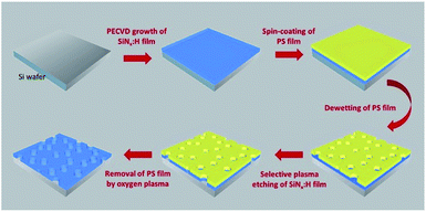
Full area Al-BSF and PERC solar cells were made from (100)-oriented, one-side polished p-type Si wafers with a thickness of 180 μm and resistivity range between 1 and 5 Ω cm. Full area Al-BSF cells were used as references. Both the saw damage removal and surface texturing were preceded at the unpolished side of a wafer using potassium hydroxide solutions. A spin-on dopant source based on phosphoric acid was developed and prepared in-house. Highly phosphorus-doped emitter layers with a sheet resistance of 60 Ω □−1 were formed on the front surface using this phosphorous source followed by diffusion at 900 °C. The junction depth from SIMS (secondary ion mass spectroscopy) analysis is around 600 nm. After that, hydrogenated silicon nitride (SiNx:H) was deposited by plasma enhanced chemical vapor deposition (PECVD) on both front and rear surface (front-side: 75 nm, back-side: 180 nm) and acts as an antireflective coating (ARC), as well as a source of hydrogen for surface passivation.In the case of PERC cells, holey PS films were used for back contact opening. The PS opening technique is sketched in Fig. 1. First, a spin-on PS solution was prepared by dissolving PS powders (Mw = 650 kg mol−1, Mw/Mn = 1.05) in toluene. 50 nm-thick PS films were coated on top of the rear passivation layer via spin-coating of the PS solution. Holey PS films, which serve as etch masks, could be obtained after immersing PS-coated wafers into acetone. The immersion time was adjusted to control the average size of holes and open-area fraction. The circular contact holes through the passivation layers can be formed by etching away exposed SiNx:H layers using Ar/SF6 plasma followed by removal of holey PS films using oxygen plasma, as depicted in Fig. 1. Then, the Ag and Al pastes were screen-printed and co-fired to form the front electrodes and back contacts, separately. The co-firing process step was performed at 800 °C for both full and local Al-BSF cells. The back-side contact exhibits a BSF thickness of approximately 6 μm. The contact resistivity of the back-side contact (∼8.8 × 10⁻³ Ω cm2) was determined using the transfer line method (TLM).18 The reference cell was fabricated as local Al-BSF cells except for rear full Al screen printing without passivation. Fig. S1† shows schematic cross-sections of both PERC and reference cells.
For the characterization, hole formation in the PS films was investigated via a scanning electron microscope (SEM) and an optical microscope (OM). The carrier lifetime was measured by quasi-steady-state photo-conductance (QSSPC) using a WCT-120 silicon wafer lifetime detector (Sinton Consulting Inc.). The illuminated current–voltage (J–V) characteristic of the fabricated solar cells was measured at room temperature under the air mass 1.5 global spectrum. The reflectance and internal quantum efficiency (IQE) of the samples were evaluated using an IPCE (Incident Photon to current Conversion Efficiency) system with a wavelength range of 300 to 1100 nm.
Results and discussion
Ultrathin polymer films on substrates are generally unstable, and their instability could be revealed through dewetting processes by immersion under a liquid solvent, resulting in a decrease in the glass transition temperature and interfacial tension, and thus formation of holes.19,20 In the solvent-driven dewetting, the short range force of polar interactions at the interfaces may be mainly responsible for the film instability instead of the apolar Lifshitz–van der Waals forces.21,22 Therefore, solvent polarity may be an important factor in the solvent-driven dewetting. In this study, the polar poor solvent (such as acetone) was chosen to carry out the dewetting process for two reasons: (1) prevention of rapid dissolution of the polymer during dewetting, and (2) promotion of film instability and dewetting by favorable polar interactions at the interface.20Fig. 2 shows the morphologies of PS films on top of SiNx-passivated Si wafers after dewetting in acetone with an immersion time of between 60 s and 600 s. Dewetting of smooth PS films begins with formation of holes. As shown in Fig. 2(a), the hole nucleation was developed at random locations throughout the surfaces of the PS films within a few seconds of immersion in acetone. The holes grow in size and remain isolated from one another at the early stages. As holes continue to grow, the rims of growing holes eventually contact each other and then the coalescence of holes occurs due to the capillary pressure (see Fig. 2b–d).23 As depicted in Fig. 2, the size distribution of the holes is relatively narrow even after immersion for 600 s, implying that all holes were created nearly simultaneously within a narrow time interval at the initial stage.
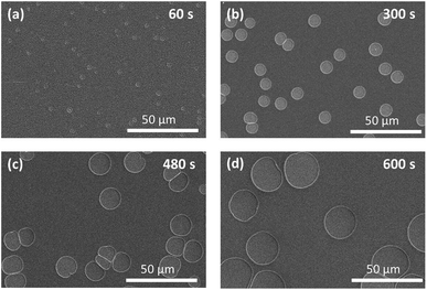 | ||
| Fig. 2 SEM images of holey PS films on top of SiNx-passivated Si wafers after immersion in acetone for (a) 60 s, (b) 300 s, (c) 480 s and (d) 600 s. | ||
The surface roughness of the PS films was evaluated as a function of immersion time by atomic force microscopy (AFM) in terms of root mean square (RMS) roughness. Representative AFM images of the surfaces of PS films before and after immersion in acetone are presented in Fig. S2(a) and (b).† As depicted in Fig. S2(c),† the RMS roughness value remains nearly unchanged after a very early stage of dewetting (immersion time < 60 s), implying that nucleated dewetting is the dominant rupture mechanism since instability amplitude of the spinodal dewetting process would grow over longer timescales and thus lead to a continuous increase in surface roughness.17
A systematic analysis of the dewetting evolution of 50 nm-thick PS films was carried out using ImageJ software. The derived average diameter of holes, hole density and open-area fraction are shown as a function of time in Fig. 3. The average diameter of holes in Fig. 2 was determined by counting at least 200 holes. From Fig. 3(a), it is clearly observed that the average size of holes increases with an increase in dewetting time, while the number of holes would gradually decrease due to coalescence of growing holes. The continued growth and coalescence of holes is also reflected in an increase in the open-area fraction (shown in Fig. 3b).
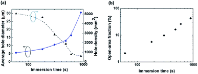 | ||
| Fig. 3 (a) Average diameter and number density of holes, and (b) open-area fraction as a function of immersion time for PS films on top of the SiNx:H passivation layers. | ||
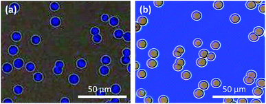
Optical microscopy was used to examine the eligibility of holey PS films serving as etch masks since a high optical contrast between Si and SiNx:H could be obtained. Fig. 4(a) shows a typical OM image of a holey PS film on the SiNx:H layer after immersion in acetone for 300 s. In this study, the thickness of all PS films was kept constant at around 50 nm, which was determined by atomic force microscope (AFM) measurements on the holey films. The holey PS film has advantageous properties as an etch mask since PS is inexpensive and chemically inert, but could be easily attacked by organic solutions and oxygen plasma. Here, the portion of the SiNx:H film not masked by the holey PS film was removed using SF6 plasma with the addition of Ar. The previous study has shown that the sputter yield of PS films by Ar ions is much less than unity after formation of a surface damaged layer with a thickness < 2 nm,24 implying that the holey PS film could serve as an etch mask for Ar/SF6 plasma etching of SiNx:H. After removal of the holey PS film by oxygen plasma, as shown in Fig. 4(b), it can be confirmed that the hole patterns in PS films can be successfully transferred to the SiNx:H layer, which indicates that highly selective etching of SiNx:H with respect to PS could be achieved.
To investigate the surface recombination properties of rear surfaces with local Al-BSF structures fabricated by the hole-patterning technique described in this study, the test wafers were coated by SiNx:H films on both sides followed by LBC fabrication with various metallization areas. Fig. 5(a) shows effective carrier lifetime (τeff) as a function of metallization area fraction (f) which was obtained from QSSPC measurements with an injection level of Δn = 1015 cm−3. The metallization areas are assumed to be the same as the exposed areas of holey PS films since the metallization patterns were defined by holey PS films. The maximum lifetime is around 40 μs for the symmetrically SiNx-passivated sample (f = 0%). In addition, the effective lifetime is gradually reduced with increasing the f value, indicating that the SiNx:H layer could provide a better passivation quality compared to Al-BSF.
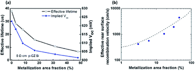 | ||
| Fig. 5 (a) Minority carrier lifetime and implied Voc as a function of metallization area fraction. (b) Effective rear-surface recombination velocity as a function of metallization area fraction. | ||
The surface recombination velocities (SRVs) can be linked to the measured τeff via25,26
 | (1) |
 | (2) |
 | (3) |
The dewetting technique was used to fabricate the LBCs for PERC solar cells with various metallization area fractions. This study concentrates on development of the local metallization technique without optimal designs and fabrication processes to enhance the cell efficiency, such as passivation and firing steps. The illuminated characteristics of fabricated PERC and reference cells (short circuit current density (Jsc), open circuit voltage (Voc), fill factor (FF) and conversion efficiency) are shown in Fig. 6 as a function of the metallization area fraction. Compared to the reference cell, a clear increase in Voc and Jsc of PERC cells could be observed as a result of the improved rear passivation, while the FF decreases with reducing the metallization area fraction, which could be mainly attributed to the parasitic resistive losses. The highest conversion efficiency is achieved from the sample with f = 8%, and its illuminated J–V curve is displayed in Fig. 7(a) and compared to that of the reference cell.
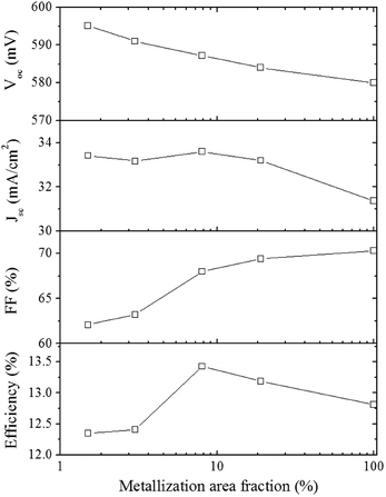 | ||
| Fig. 6 One-sun illuminated cell parameters (Voc, Jsc, FF, and efficiency) of reference (full-area Al-BSF) and PERC solar cells with various rear metallization area fractions. | ||
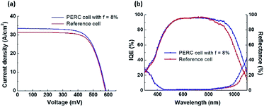 | ||
| Fig. 7 (a) Illuminated J–V characteristics and (b) IQE and reflectance of the reference cell and PERC cell with f = 8%. | ||
In order to evaluate rear-side passivation properties, IQE and reflectance measurements were performed on both the reference and PERC cells. As depicted in Fig. 7(b), the IQE spectra of the reference and the PERC cells under front side illumination overlap from the near ultraviolet to the visible regime, while the distinct difference was measured in the near infrared above 850 nm. The longer wavelength part of the IQE spectrum is sensitive to the quality of rear-side passivation layers which is mainly characterized by the two parameters: rear-side SRV and the light reflectance on the rear.31,32 For the PERC samples, the higher IQE values in the wavelength range between 800 nm and 1000 nm is reflected in a lower rear-side SRV, which is corresponding to the results in Fig. 5(b). In addition to reducing carrier combination, the passivation layers could simultaneously increase internal reflection of the light on rear surface, which results in an increase in the escape reflectance and IQE at wavelengths above 1000 nm. From these experimental results, the improvements in the Voc and Jsc could be ascribed to less recombination losses and the improved rear reflectance of PERC cells. As discussed above, a reduction in the metallization area fraction could decrease the rear surface recombination but increase the series resistance, which in turn increases both Voc and Jsc but lowers the FF. Therefore, the optimal metallization area is determined by trade-off between the surface recombination and resistive losses. In this report, the best PERC cell shows a conversion efficiency of 13.4% with an obvious increase in Voc and Jsc of 7 mV and 2.1 mA cm−2, respectively, leading to a gain of 0.6% absolute in efficiency compared to the reference cell. From the previous studies, the laser-based PERC processes could result in an improvement in cell efficiency ranging between 0.6% and 1%,33–36 implying that the dewetting technique could be a promising approach for PERC fabrication while the reported cell results were based on preliminary, non-optimal fabrication processes. Further improvement in process parameters (firing, diffusion and doping conditions, etc.) is likely to enhance the cell performance, as well as the efficiency gain.
Conclusions
In this report, we have investigated the feasibility of dewetting of PS films as an approach to fabricate local metal–semiconductor contacts for Si PERC solar cells. Dewetting of PS films on dielectric-passivated Si wafers could lead to the formation of circular holes in PS films, which were served as etch masks to create local contact patterns after plasma etching. The metallization area could be well-controlled by adjusting the dewetting time. Furthermore, this simple patterning technique could effectively minimize surface damage during the metallization process. Compared to the fully area BSF cell, an apparent increase in efficiency of up to 0.6% could be achieved due to better rear passivation and higher rear internal reflectance, indicating that the dewetting technique is well suited for implementing the local contact patterns and has the promising potential for application in fabrication of PERC cells.Conflicts of interest
There are no conflicts to declare.Acknowledgements
This work was supported by the Ministry of Science and Technology of Taiwan under grant numbers 107-2221-E-008-008, 107-2622-E-008-018-CC3 and 108-3116-F-008-008.References
- A. W. Blakers, A. Wang, A. M. Milne, J. Zhao and M. A. Green, Appl. Phys. Lett., 1989, 55, 1363–1365 CrossRef CAS.
- R. Preu, S. W. Glunz, S. Schäefer, R. Lcdemann, W. Wettling and W. Pfleging, Proc. 16th Eur. Photovoltaic Sol. Energy Conf., 2000, pp. 1181–1184 Search PubMed.
- G. Agostinelli, J. Szlufcick, P. Choulat and G. Beaucarne, Proc. 20th Eur. Photovoltaic Sol. Energy Conf., 2005, pp. 942–945 Search PubMed.
- E. Schneiderlochner, R. Preu, R. Lüdemann and S. W. Glunz, Prog. Photovoltaics Res. Appl., 2002, 10, 29–34 CrossRef CAS.
- E. Lohmüller, B. Thaidigsmann, M. Pospischil, U. Jäger, S. Mack, J. Specht, J. Nekarda, M. Retzlaff, A. Krieg, F. Clement, A. Wolf, D. Biro and R. Preu, IEEE Electron Device Lett., 2011, 32, 1719–1721 Search PubMed.
- B. Vermang, H. Goverde, A. Uruena, A. Lorenz, E. Cornagliotti, A. Rothschild, J. John, J. Poormans and R. Mertens, Sol. Energy Mater. Sol. Cells, 2012, 101, 204–209 CrossRef CAS.
- C. H. Hsu, C. H. Yang, Y. H. Wang, C. W. Huang, S. Y. Lien, C. Y. Kung and J. C. Lou, Materials, 2016, 9, 549 CrossRef PubMed.
- Z. R. Du, N. Palina, J. Chen, F. Lin, M. H. Hong and B. Hoex, 27th Eur. Photovolt Sol. Energy Conf., 2012, pp. 1230–1233 Search PubMed.
- J. M. Yacob Ali, V. Shanmugam, B. Lim, A. G. Aberle and T. Mueller, Sol. Energy, 2018, 164, 287–291 CrossRef CAS.
- K. Jacobs and S. Herminghaus, Langmuir, 1998, 14, 965–969 CrossRef CAS.
- R. Seemann, S. Herminghaus and K. Jacobs, J. Phys.: Condens. Matter, 2001, 13, 4925–4938 CrossRef CAS.
- L. J. Xue and Y. C. Han, Prog. Polym. Sci., 2011, 36, 269–293 CrossRef CAS.
- A. Sehgal, V. Ferreiro, J. F. Douglas, E. J. Amis and A. Karim, Langmuir, 2002, 18, 7041–7048 CrossRef CAS.
- Z. X. Zhang, Z. Wang, R. B. Xing and Y. C. Han, Polymer, 2003, 44, 3737–3743 CrossRef CAS.
- D. Julthongpiput, W. Zhang, J. F. Douglas, A. Karim and M. J. Fasolka, Soft Matter, 2007, 3, 613–618 RSC.
- A. Verma and A. Sharma, Adv. Mater., 2010, 22, 5306–5309 CrossRef CAS PubMed.
- G. Amarandei, C. O'Dwyer, A. Arshak and D. Corcoran, Soft Matter, 2013, 9, 2695–2702 RSC.
- D. L. Meier and D. K. Schroder, IEEE Trans. Electron Devices, 1984, 31, 647–653 Search PubMed.
- L. Xu, A. Sharma and S. W. Joo, Macromolecules, 2012, 45, 6628–6633 CrossRef CAS.
- L. Xu, A. Sharma, S. W. Joo, H. Liu and T. Shi, Langmuir, 2014, 30, 14808–14816 CrossRef CAS PubMed.
- A. Sharma and A. T. Jameel, J. Colloid Interface Sci., 1993, 161, 190–208 CrossRef CAS.
- A. Sharma and R. Khanna, Phys. Rev. Lett., 1998, 81, 3463–3466 CrossRef CAS.
- A. Sharma and G. Reiter, J. Colloid Interface Sci., 1996, 178, 383–399 CrossRef CAS.
- J. J. Végh, D. Nest, D. B. Graves, R. Bruce, S. Engelmann, T. Kwon, R. J. Phaneuf, G. S. Oehrlein, B. K. Long and C. G. Willson, Appl. Phys. Lett., 2007, 91, 233113 CrossRef.
- K. L. Luke and L. J. Cheng, J. Appl. Phys., 1987, 6, 2282–2293 CrossRef.
- A. B. Sproul, J. Appl. Phys., 1994, 76, 2851–2854 CrossRef CAS.
- J. Müller, K. Bothe, S. Gatz, F. Haase, C. Mader and R. Brendel, J. Appl. Phys., 2010, 108, 124513 CrossRef.
- R. H. Cox and H. Strack, Solid-State Electron., 1967, 10, 1213–1218 CrossRef.
- M. Rahman, J. Appl. Phys., 1997, 82, 2215–2224 CrossRef CAS.
- N. G. Stoffel, S. A. Schwartz, M. A. A. Pudensi, K. Kash, L. T. Florez, J. P. Harbison and B. J. Wilkens, Appl. Phys. Lett., 1992, 60, 1603–1605 CrossRef CAS.
- M. Schaper, J. Schmidt, H. Plagwitz and R. Brendel, Prog. Photovoltaics Res. Appl., 2005, 13, 381–386 CrossRef CAS.
- J. H. Lai, A. Upadhyaya, S. Ramanathan, A. Das, K. Tate, V. Upadhyaya, A. Kapoor, C. W. Chen and A. Rohatgi, IEEE J. Photovolt., 2011, 1, 16–21 Search PubMed.
- K. Wijekoon, F. Yan, Y. Zheng, D. Wang, H. Mungekar, L. Zhang and H. Ponnekanti, Int. J. Photoenergy, 2013, 368403 Search PubMed.
- H. Yang, E. Wang, H. Wang and W. Guo, Energy Procedia, 2016, 88, 389–393 CrossRef CAS.
- E. Wang, H. Wang and H. Yang, Int. J. Photoenergy, 2016, 8982376 Search PubMed.
- A. Kumar, M. Bieri, T. Reindl and A. G. Aberle, Energy Procedia, 2017, 130, 43–49 CrossRef.
Footnote |
| † Electronic supplementary information (ESI) available. See DOI: 10.1039/c9ra10457g |
| This journal is © The Royal Society of Chemistry 2020 |

