
 Open Access Article
 This Open Access Article is licensed under a Creative Commons Attribution-Non Commercial 3.0 Unported Licence
Effect of co-sensitization of InSb quantum dots on enhancing the photoconversion efficiency of CdS based quantum dot sensitized solar cells
T. Archanaa,
K. Vijayakumara,
G. Subashinib,
A. Nirmala Graceb,
M. Arivanandhan *a and
R. Jayavela
*a and
R. Jayavela
aCentre for Nanoscience and Technology, Anna University, Chennai-600025, Tamil Nadu, India. E-mail: arivucz@gmail.com; Tel: +91 44 22359114
bCentre for Nanotechnology Research, Vellore Institute of Technology, Vellore-632014, Tamil Nadu, India
First published on 14th April 2020
Abstract
The effect of co-sensitization of CdS and InSb Quantum Dots (QDs) on the enhancement of efficiency of Quantum Dots Sensitized Solar Cells (QDSSCs) has been investigated. InSb is synthesized by a facile solvothermal method using indium metal particles and antimony trichloride as precursors. From TEM images the average particle size of InSb was found to be less than 25 nm. The I–V data showed photoconversion efficiency (PCE) of 0.8% using InSb QDs as a sensitizer layer for QDSSC. However, co-sensitization of InSb QDs and CdS QDs on the TiO2 photoanode in QDSSCs showed an enhanced PCE of 4.94% compared to that of CdS sensitized solar cells (3.52%). The InSb QD layer broadens the light absorption range with reduced spectral overlap causing an improvement in light harvesting along with suppression of surface defects which reduced the recombination losses. As a result, co-sensitized TiO2/CdS/InSb QDSSC exhibits a greatly improved PCE of 4.94%, which is 40% higher than that of TiO2/CdS (3.52%) based QDSSCs due to improved light absorption with low recombination losses.
1. Introduction
Dye sensitized solar cells (DSSCs) (Gratzel cells) and quantum dot sensitized solar cells (QDSSCs) are promising solar cell technologies as they utilize dye and quantum dots (QDs) as light sensitizing materials.1–7 DSSCs have several limitations such as poor stability of the dye molecules, high cost of dyes, and single wavelength absorption which restricts their applications,8 whereas QDs exhibit excellent properties like tunable bandgap, multiple carrier generation and high absorption coefficient. Therefore, QDs based sensitized solar cells are more promising compared to DSSCs. However, the QDSSCs fall behind in conversion efficiency compared to DSSCs.9,10 The QDs are semiconductor nanoparticles having dimensions less than their exciton bohr radius. However, the exciton bohr radius of widely used semiconductor QDs such as CdS (3.4 nm), CdSe (6.1 eV) and PbS (20 nm) are less than 20 nm. So, the tunability of their properties within the confinement regime is difficult. Moreover, most of QDs (CdS, PbS, CdSe) used for sensitized solar cells are active in the visible region.11The low efficiency of QDSSCs are partially associated with the performance of sensitizer materials which are mostly active only in the visible regime of solar light spectrum and hence light absorption get confined at wavelength less than 700 nm.12,13 For improved light absorption with wider coverage of solar spectrum, co-sensitization of QDs can be a promising approach in the field of QDSSCs. Hence the strategy to improve light absorption apart from visible regime could possibly enhance the photoconversion efficiency of QDSSCs.14–16 In this aspects, Xueyi Guo et al. reported co-sensitization of N719 dye with Ag2Se QDs showed an efficiency of 3.23%.15 Yibing Lin et al. reported co-sensitization of CdS and CdSe QDs with an improved efficiency of 4.2.16 Dong Liu et al. reported 3.95%, PCE for the co-sensitization of CdS and CdSe QDs on a comparative study using Pt and CuS counter electrode.17 Hwang et al. reported the significant improvement of photocurrent density (27.6 mA) of QDSSC by co-sensitization of Ag2S with CdS QDs.18 From the literature, it is obvious that the co-sensitization is a promising approach compared to single sensitizer (CdS or PbS or CdSe) for improving the performance of QDSSCs.19 Tung et al. reports on control on recombination achieved by co-sensitized structure.20,21 Most of the literatures highlight on UV-Vis active material as co-sensitizer for sensitized solar cells with an objective to improve the efficiency. Whereas, the visible (44%) and infrared (53%) radiations dominate the solar spectrum which covers from 280 to 2700 nm.22–24 Therefore, effective utilization of IR region by means of IR active QDs could enhance the efficiency of the QDSSC. However, co-sensitization of IR active QD material with visible active material for solar cell applications are rarely investigated.
Indium antimonide (InSb) is one of the narrow band gap (0.17 eV) semiconductors with large exciton bohr radius of 68.5 nm. Therefore, the properties of InSb QDs can be tuned by changing its size in the confinement regime.15 Moreover, InSb has been reported to be an efficient IR active material as it possesses narrow band gap. InSb QDs are notable for their promising ability to efficiently harvest the near infrared region of solar spectrum and therefore achieving more coverage of solar spectrum.25 Co-sensitization of InSb with visible active QDs could enhance the quantum efficiency of QDSSC. However, co-sensitization of InSb QDs with other semiconducting QDs are not reported in the literature.26–28 Henceforth InSb can be studied as viable sensitizer material for QDSSC applications.
Hitherto InSb QDs and its applications are scarcely ever considered as they are highly reactive towards air and moisture due to co-valent nature of group III–V elements.29–32 Most of works reported on in situ growth and deposition of InSb thin films.33–36 Only few works have been reported on the synthesis of InSb QDs.37,38 Therefore, in the present work, the growth conditions for the formation of InSb QDs were initially optimized and examined its suitability as a photo sensitizer for different QDSSC cell structures with and without co-sensitization of CdS. The co-sensitized TiO2/CdS/InSb QDSSC exhibits a greatly improved PCE of 4.94%, which is 40% higher than that of TiO2/CdS (3.52%) based QDSSC.
2. Experimental
2.1 Synthesis of InSb quantum dots
High purity indium particles (99.99%) (Merck), antimony trichloride (SbCl3) (TCI Chemicals), xylene (Alfa Aesar) and ethanol (Honeywell) were procured and used as source materials without further purification.InSb QDs were synthesised by solvothermal self-reduction method using high purity In metals and SbCl3 as precursors. In and SbCl3 were taken in a molar ratio of 1![[thin space (1/6-em)]](https://www.rsc.org/images/entities/char_2009.gif) :2 and dissolved in 100 ml of xylene in polypropylene lined (PPL) vessel filled to 70% of the total volume with xylene. The vessel was sealed into a stainless-steel tank and maintained at 280 °C for 15 h. After completion of solvothermal reaction, autoclave was allowed to cool to room temperature and resulted product was filtered off, washed with double distilled water and absolute ethanol. The resulted blackish brown product was isolated by centrifugation at 8000 rpm and transferred to Petri dish and vacuum dried at 80 °C for 3 h.38–40 The obtained InSb nanostructures were characterized for morphological and structural analysis.
:2 and dissolved in 100 ml of xylene in polypropylene lined (PPL) vessel filled to 70% of the total volume with xylene. The vessel was sealed into a stainless-steel tank and maintained at 280 °C for 15 h. After completion of solvothermal reaction, autoclave was allowed to cool to room temperature and resulted product was filtered off, washed with double distilled water and absolute ethanol. The resulted blackish brown product was isolated by centrifugation at 8000 rpm and transferred to Petri dish and vacuum dried at 80 °C for 3 h.38–40 The obtained InSb nanostructures were characterized for morphological and structural analysis.
2.2 Characterization of InSb quantum dots
The structural properties of the InSb samples obtained by solvothermal synthesis at were examined by X-ray diffraction (XRD) analysis using X-ray diffractometer (Bruker D8 advance diffractometer) with Cu Kα (1.54 Å) radiation. The X-ray diffraction pattern was recorded in the range of 2θ from 10 to 80 with a stepwise increment of 0.02 and a count time of 5 s. Morphology of vacuum dried InSb samples were investigated using high resolution scanning electron microscope with energy-dispersive X-ray analysis (HR SEM-FEI Quanta FEG 200). Further, the shape and size of InSb sample were analysed by high resolution transmission electron microscopy (HRTEM; JEOL TEM 2400). The UV-Vis-NIR absorption spectrum of InSb was recorded using PerkinElmer Optima 5300 DV UV-Vis-NIR spectrophotometer. XPS analysis of prepared samples was carried out by Shimadzu ESCA 3400 X-ray photoelectron spectrophotometer. Electrochemical impedance spectra (EIS) of the prepared electrodes were recorded by CHI electrochemical workstation (CHI 1106C) at frequency ranging from 10 MHz to 100 kHz and impedance spectra were analyzed with EC lab software.2.3 Fabrication of QDSSC
Titanium tetraisopropoxide (Sigma Aldrich), nitric acid (Alfa Aesar), ethanol (Honeywell), acetic acid (Alfa Aesar), FTO glass slides (7 Ω resistance, Sigma Aldrich), chloroplatinic acid (Sigma Aldrich), ethyl cellulose (TCI Chemicals), alpha-terpinol (TCI Chemicals), acetone, cadmium chloride (Alfa Aesar), sodium sulphide (TCI Chemicals), copper acetate (Alfa Aesar) were procured and used as source materials without further purification.The paste was coated over conducting side of FTO glass plate for area of 0.16 cm2. The coated glass slide was dried at 100 °C for 30 minutes and calcined at 450 °C for 15 minutes and slowly cooled down to room temperature.
3. Results and discussions
3.1 Structural and morphological analysis
The X-ray diffraction (XRD) pattern of InSb QDs is shown in Fig. 1. The diffraction pattern is well matched with cubic zinc blende structure of InSb, in addition with a few low intensity peaks of Sb. The obtained cell parameter (a = 6.4781) is in good agreement with the standard JCPDS data (card no. 6-208). From XRD pattern (Fig. 1), the size of the crystallites of InSb QDs was calculated to be 37.16 nm using Scherrer equation.33,45,46,54 Morphology of InSb QDs was studied by FESEM and shown in Fig. 2a. Spherical morphology of the InSb QDs can be seen from FESEM images and Fig. 2b shows EDS spectrum of the sample. The strong peaks corresponding to In and Sb are clearly observed. The composition of the prepared InSb is confirmed by EDS spectrum.30,31 | ||
| Fig. 1 XRD pattern of InSb quantum dots. | ||
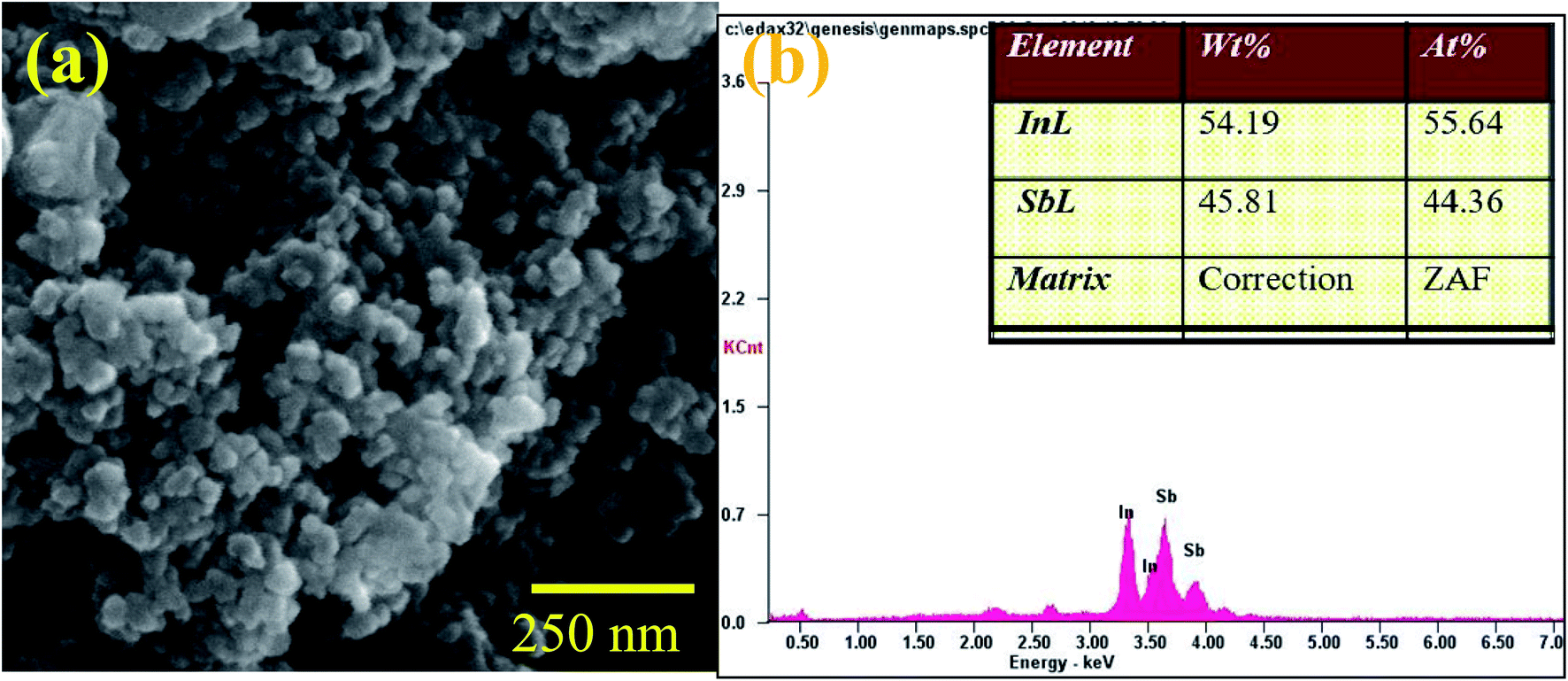 | ||
| Fig. 2 (a) SEM image (b) EDAX spectrum of InSb QDs. | ||
Typical HRTEM images of the InSb samples are shown in Fig. 3a and b. The size and morphology of QDs can be clearly identified using TEM images. The nanocrystalline InSb had plate-like and spherical morphology as shown in Fig. 3a and b. The average size of InSb nanocrystals was found to be less than 25 nm which confirms the formation of InSb QDs as the size is less than its exciton bohr radius (68.5 nm). The HRTEM image (Fig. 3c) of InSb QDs shows the clear lattice fringes which confirm its crystalline nature. The interplanar spacing of InSb QDs was measured at two different places as 0.38 nm and 0.32 nm corresponds to (111) and (200) lattice planes, respectively.
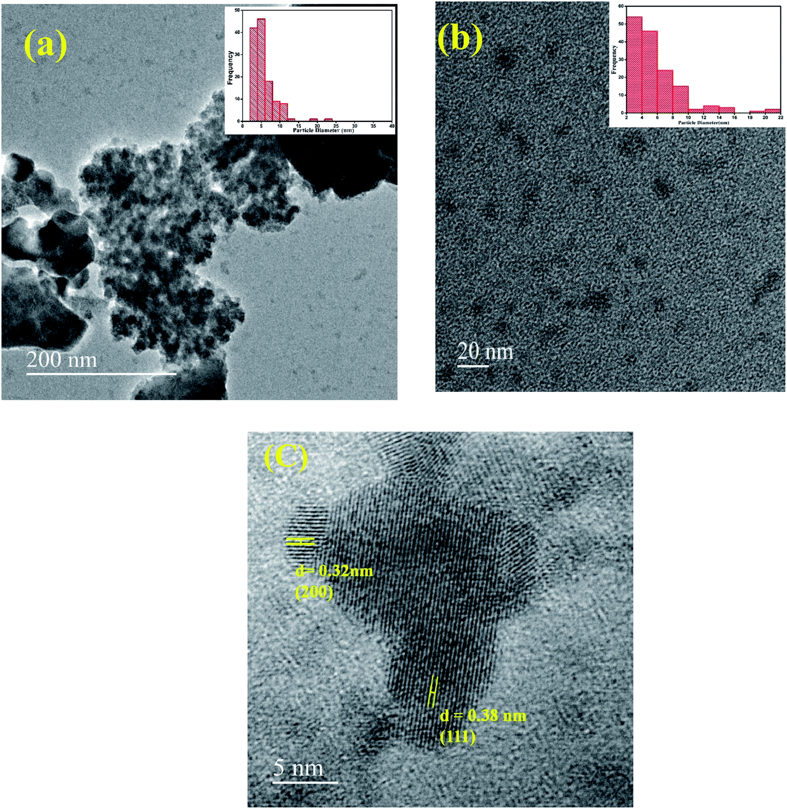 | ||
| Fig. 3 (a and b) TEM images of InSb QDs (inset of (a) and (b) are histogram for particle size distribution) (c) HRTEM image of InSb QDs. | ||
3.2 XPS analysis
The XPS spectra of InSb QDs are shown in Fig. 4a and b. The core level spectrum of In (Fig. 4a) shows the doublet peaks of In 3d5/2 and In 3d3/2 at 445.57 and 453.22 eV, respectively. The doublet peaks are separated with the binding energy of 7 eV which arises from spin–orbit-splitting. Fig. 4b shows the core level spectrum of antimony shows two peaks at 532.08, and 540.8 eV respectively. XPS further confirms the formation of InSb. Semiquantitative analysis of the peaks gave the ratio of In to Sb as 52.3:47.7.38,48
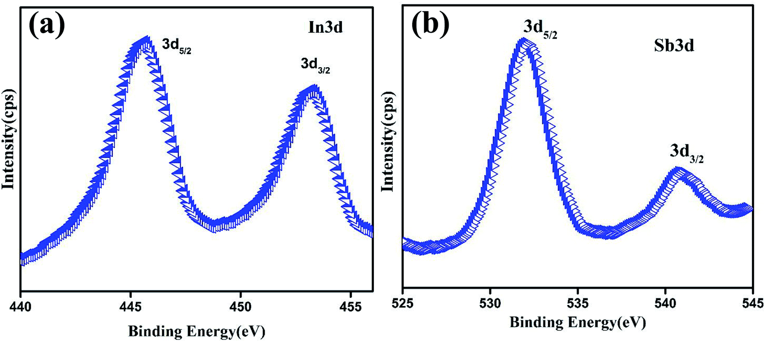 | ||
| Fig. 4 XPS spectra of (a) In 3d and (b) Sb 3d of InSb quantum dots. | ||
3.3 Optical studies
Fig. 5 shows the optical absorption spectrum of InSb QDs which reveals a wide range of absorption in the near IR region. From the UV-Vis-NIR spectrum, absorption maximum can be seen to be at 870 nm and slightly decreasing towards high wavelength. On plotting Tauc plot the estimated bandgap energy is found to be 1.01 eV (inset of Fig. 5). The band gap for InSb QDs seems to be widened from 0.17 eV to 1.01 eV because of the quantum confinement effect.44 Optical absorption of InSb QDs shift towards near-infrared thereby significantly enhance current density by reducing UV absorption loss which occurs during light absorption and thus favouring conduction process under light illumination.12–14,23,31,42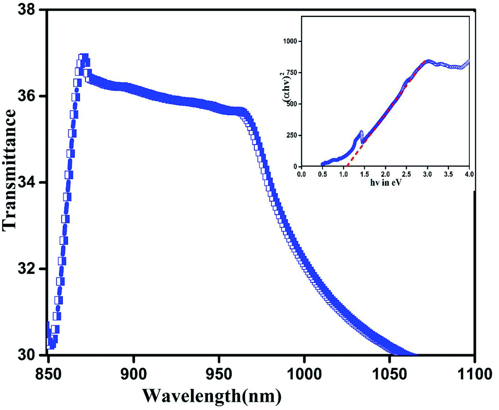 | ||
| Fig. 5 UV-Vis-NIR absorption spectrum (inset-Tauc plot) of InSb QDs. | ||
3.4 Photoanode characterization
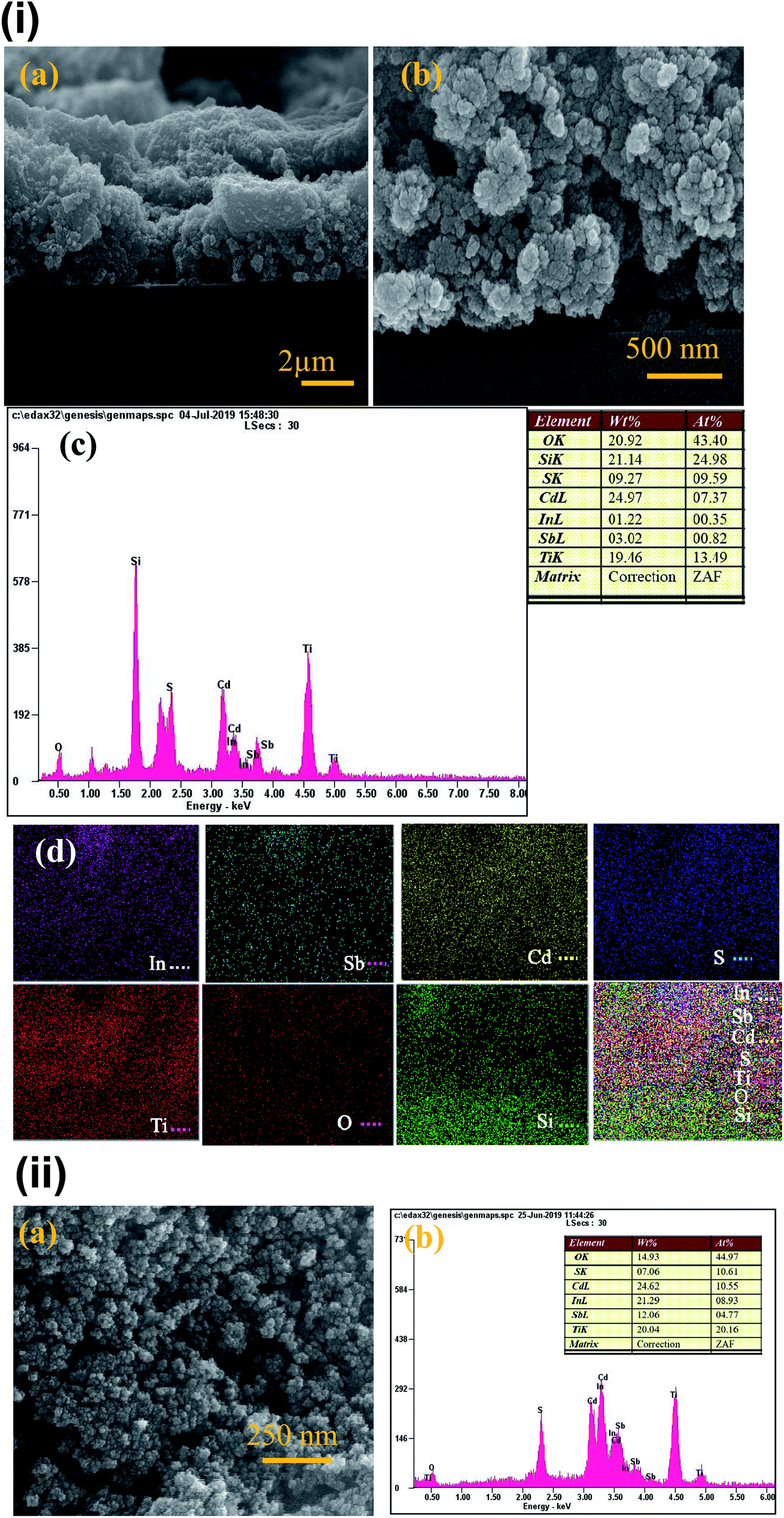 | ||
| Fig. 6 (i) (a and b) FESEM images, (c) EDAX with elemental composition and (d) EDAX elemental mapping of cross-sectional surface of co-sensitized InSb/CdS loaded TiO2 photoanode. (ii) (a) FESEM image (b) EDAX with elemental composition of surface of co-sensitized InSb/CdS loaded TiO2 photoanode. | ||
 | ||
| Fig. 7 (a) UV-Vis-NIR DRS and (b) photoluminescence spectra of CdS and InSb QDs loaded TiO2. | ||
The emission at two different wavelengths is due to difference in band gap of CdS and InSb as seen by difference in absorption occurring at visible and NIR region.52–54 The PL study demonstrated that the emission performance can be enhanced by co-sensitization of QDs and thus recombination of surface trapped electrons can be relatively suppressed. The PL peaks of TiO2/CdS/InSb photoanode are relatively boarder, which may be due to the band matching. The band alignment favours the transfer of electrons from the InSb and CdS QD sensitizer layers towards photoanode layer, inducing reduced charge recombination.
3.5 EIS analysis of photoanodes
Electrochemical impedance spectroscopy (EIS) analysis is used to evaluate the internal resistance and charge transfer kinetics of fabricated photoanodes. Fig. 8(i) shows the Nyquist plots of TiO2/CdS and TiO2/CdS/InSb photoanodes. The plots were analysed using EC lab software with an equivalent circuit. From EIS data, it is clear that the TiO2/CdS electrode shows relatively higher series resistance compared to TiO2/CdS/InSb co-sensitized photoanode. From EIS spectra, it is also confirmed that the TiO2/CdS/InSb co-sensitized photoanode shows low charge transfer resistance compared to TiO2/CdS electrode which favors for high performance of QDSSC with co-sensitized photoanodes. The inset table shows the measured series resistance and charge transfer resistance of the electrodes. The low series resistance and charge transfer resistance of the co-sensitized photoanodes are originated from the narrow band gap InSb QDs.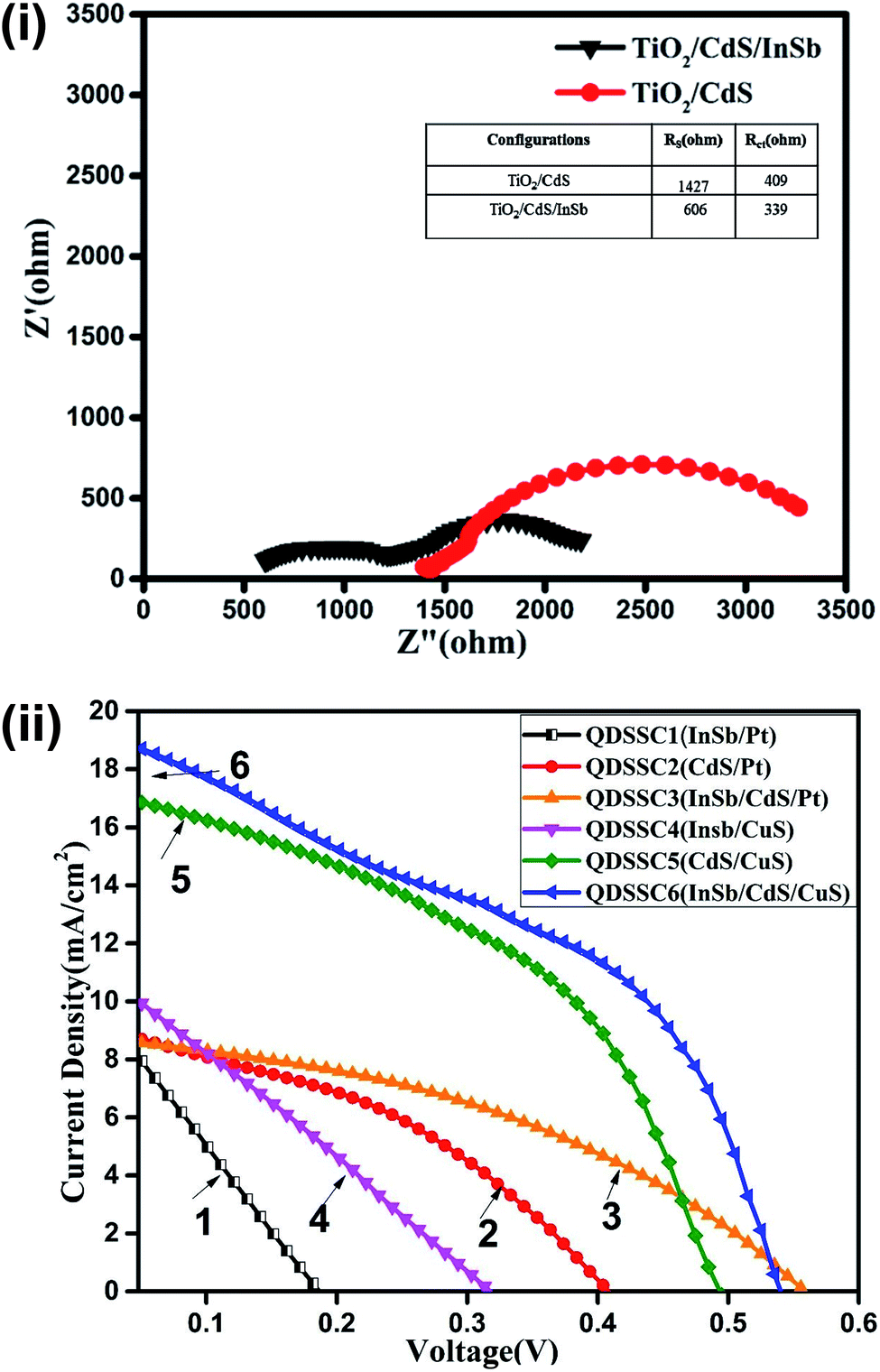 | ||
| Fig. 8 (i) Nyquist plot of QDSSC cells with platinum counter electrode. (ii) I–V characteristics of fabricated QDSSCs with different configurations. | ||
3.6 I–V measurement
The I–V characteristics of fabricated QDSSCs were analysed using a standard (AM1.5) Solar Simulator (Oriel Class AAA) under 1 sun illumination condition. The obtained cell parameter values are shown in Table 1. Fig. 8(ii) shows the I–V curves of bare InSb QDs, CdS QDs and InSb/CdS co-sensitized QDs based QDSSCs fabricated using TiO2 as photoanodes and platinum and CuS as counter electrodes. As can be seen from Fig. 8(ii), the QDSSC with CuS counter electrode showed relatively better performance compared to Pt counter electrodes for all the cell configurations. This is obviously because of better compatibility of polysulphide electrolyte with CuS counter electrode than that with platinum counter electrode. High electrocatalytic activity of CuS electrode reduces charge transfer resistance at electrolyte/electrode interface and thus not only reduces internal resistance but also enhances cell performance.47 From the I–V curves, it can be inferred that the QDSSC fabricated using InSb QDs with platinum counter electrode have shown an efficiency of 0.51% and the cell with CuS counter electrode shows the efficiency of 0.8%. While I–V characteristics of CdS based QDSSCs shows an efficiency of 1.25% for platinum and 3.52% for CuS counter electrode.| Cell | Cell configuration | Voc (V) | Jsc (mA cm−2) | Fill factor (%) | Efficiency (%) |
|---|---|---|---|---|---|
| QDSSC1 | TiO2/InSb/Pt | 0.186 | 10.96 | 24.80 | 0.51 |
| QDSSC2 | TiO2/CdS/Pt | 0.367 | 8.83 | 38.39 | 1.25 |
| QDSSC3 | TiO2/CdS/InSb/Pt | 0.516 | 8.63 | 39.76 | 1.77 |
| QDSSC4 | TiO2/InSb/CuS | 0.287 | 10.71 | 26.24 | 0.81 |
| QDSSC5 | TiO2/CdS/CuS | 0.454 | 16.98 | 45.68 | 3.52 |
| QDSSC6 | TiO2/CdS/InSb/CuS | 0.533 | 18.58 | 49.88 | 4.94 |
Co-sensitization of CdS and InSb in QDSSC with CuS counter electrode showed an efficiency (4.94%), which is significantly enhanced compared to all other cell structures (Table 1). Further the I–V curves demonstrated the relative enhancement of photocurrent density (Jsc) (18.58 mA cm−1) and fill factor (0.49) on co-sensitization which may be originated from the broadened light absorption spectrum of co-sensitizers as seen from UV-Vis-NIR spectra (Fig. 7a). Wide solar spectrum coverage provides opportunities for more electronic excitation of QDs at different energy levels thereby generating multiple excitons. The band matching achieved by each QD layer without spectral overlap favours electron hopping at a faster rate towards the photoanode which improved photocurrent density.
The open circuit voltage (Voc) of the QDSSC has been improved for the co-sensitizer compared to single sensitizer based QDSSCs. In general Voc is mainly affected by the recombination losses that can deliberately downturn excitonic life time of charge carries. A significant improvement in Voc is observed for co-sensitization of IR active InSb with visible active CdS QDSSCs illustrated the low recombination losses in co-sensitized QDSSCs. InSb QDs act as an efficient light absorber and passivating layer for SILAR deposited CdS in the photoanodes thereby decreasing the surface trap sites as seen from PL spectra in Fig. 7b. In addition, the InSb layer prevents retention of electrolyte towards sensitizer and hence much better control on recombination process was resulted.39 Furthermore, the TiO2/CdS/InSb photoanodes shows relatively low charge transfer resistance and low series resistance as observed from EIS spectras (Fig. 8(i)) which ease the charge transport in the fabricated QDSSCs. Therefore, the InSb co-sensitized QDSSC shows high efficiency of 4.94%. The obtained efficiency is relatively higher than that of reported co-sensitized QDSSC.16,17 The experimental results demonstrated that the co-sensitization of IR active InSb QDs with CdS is a promising approach to improve the performance of QDSSC.
4. Conclusions
InSb QDs has been successfully synthesized by solvothermal method. The structural, morphological and optical properties of InSb QDs were investigated. To improve the efficiency of QDSSC, the IR active InSb QDs were effectively co-sensitized with CdS QDs and studied their I–V characteristics. The I–V results indicated that the InSb QD co-sensitized QDSSC shows relatively higher efficiency of 4.94% compared to CdS QD based QDSSC (3.5%). Moreover, the co-sensitization of InSb QDs, effectively improved the current density, Jsc (18.57 mA cm−2) and open circuit voltage, Voc (533 mV) of QDSSC which resulted the high efficiency. The co-sensitization of InSb QDs improved the absorption of solar energy and suppressed the recombination losses which improved the cell performance. Therefore, the present study emphasizes the potential of co-sensitization of InSb QDs for QDSSC applications.Conflicts of interest
There is no conflict to declare.Acknowledgements
The author (T. A.) is grateful to Department of Science & Technology for grant (SR/WOS-A/ET-40/2017(G)) under Women Scientists Scheme A (WOS-A). Authors also acknowledge the financial support of DST-SERB under ECR award (ECR/2015/000575) and EMR (EMR/2016/007550).References
- O. Ellabban, H. Abu-Ru and F. Blaabjerg, Renewable Sustainable Energy Rev., 2014, 39, 748–764 CrossRef.
- Z. Ning, H. Dong, Q. Zhang, O. Voznyy and H. Edward Sargent, ACS Nano, 2014, 8(10), 10321–10327 CrossRef CAS PubMed.
- A. Lennon, J. Colwell and K. P. Rodbell, Prog. Photovoltaics Res. Appl., 2019, 27, 67–97 CrossRef CAS.
- A. Mohammad Bagher, Am. J. Optic. Photon., 2015, 3, 94 CrossRef.
- M. A. Green and S. P. Bremner, Nat. Mater., 2016, 16, 23–34 CrossRef PubMed.
- M. Law, L. E Greene, J. C. Johnson, R. Saykally and P. Yang, Nat. Mater., 2005, 4(6), 455 CrossRef CAS PubMed.
- A. Kojima, K. Teshima, Y. Shirai and T. Miyasaka, J. Am. Chem. Soc., 2009, 131, 6050–6051 CrossRef CAS PubMed.
- X. Ye, M. Wen, J. Wang, N. Iocozzia, C. Zhang and Z. Lin, Mater. Today, 2015, 18, 155–162 CrossRef.
- C. Xiang, X. Zhao, L. Tan, J. Ye, S. Wu, S. Zhang and L. Sun, Nano Energy, 2019, 55, 269–276 CrossRef CAS.
- X. Zhang, X. Huang, Y. Yang, S. Wang, Y. Gong, Y. Luo, D. Li and Q. Meng, ACS Appl. Mater. Interfaces, 2013, 5, 5954–5960 CrossRef CAS PubMed.
- S. Kumar, M. Nehra, A. Deep, D. Kedia, N. Dilbaghi and K. H. Kim, Renewable Sustainable Energy Rev., 2017, 73, 821–839 CrossRef CAS.
- A. Maurice, M. L. Haro, B. Hyot and P. Reiss, Part. Part. Syst. Char., 2013, 30, 828–831 CAS.
- M. Yarema and M. V. Kovalenko, Chem. Mater., 2013, 25, 1788–1792, DOI:10.1021/cm400320r.
- F. Hatami, S. M. Kim, H. B. Yuen and J. S. Harris, Appl. Phys. Lett., 2006, 89, 133115 CrossRef.
- Q. Tian, D. Deng, Z. Zhang, Y. Li, Y. Yang and X. Guo, J. Mater. Sci., 2017, 52, 12131–12140 CrossRef CAS.
- Y. Lin, Y. Lin, J. Wu, X. Zhang and B. Fang, Appl. Phys. A: Mater. Sci. Process., 2017, 123, 1–6 Search PubMed.
- D. Liu, J. Liu, J. Liu, S. Liu, C. Wang, Z. Ge, X. Hao, N. Du and H. Xiao, J. Mater. Sci., 2019, 54, 4884–4892 CrossRef CAS.
- I. Hwang, M. Seol, H. Kim and K. Yong, Appl. Phys. Lett., 2013, 103, 023902 CrossRef.
- N. Balis, V. Dracopoulos, K. Bourikas and P. Lianos, Electrochim. Acta, 2013, 91, 246–252 CrossRef CAS.
- D. Wang, F. Yin, Z. Du, D. Han and J. Tang, J. Mater. Chem. A, 2019, 7, 26205–26226 RSC.
- H. T. Tung, N. T. Thao and L. Q. Vinh, Int. J. Photoenergy, 2018, 2018, 8545207 CrossRef.
- M. Panthakkal, A. Muthalif, Y. Lee, C. Damodharan and H. Kim, Appl. Surf. Sci., 2017, 396, 582–589 CrossRef.
- V. Tasco, N. Deguffroy, A. N. Baranov, E. Tournié, B. Satpati, A. Trampert, M. Dunaevski and A. Titkov, J. Cryst. Growth, 2007, 301, 713–717 CrossRef.
- A. T. Vogel, J. De Boor, M. Becker, J. V. Wittemann, S. L. Mensah, P. Werner and V. Schmidt, Nanotechnology, 2011, 22(1), 15605 CrossRef PubMed.
- Z. Pan, H. Zhang, K. Cheng, Y. Hou, J. Hua and X. Zhong, ACS Nano, 2012, 6, 3982–3991 CrossRef CAS PubMed.
- Y. You, X. Tong, W. Wang, J. Sun, P. Yu, H. Ji, X. Niu and Z. M. Wang, Adv. Sci., 2019, 6(9), 1801967 CrossRef PubMed.
- T. Wang, R. Vaxenburg, W. Liu, S. M. Rupich, E. Lifshitz, A. L. Efros, D. V. Talapin and S. J Sibener, ACS Nano, 2014, 9(1), 725–732 CrossRef PubMed.
- W. Sukkabot, Mater. Sci. Semicond. Process., 2014, 27, 51–55 CrossRef CAS.
- D. Li, H. Li, H. Sun and L. Zhao, Nanoscale Res. Lett., 2011, 6(1), 601 CrossRef PubMed.
- M. S. Atoyan, E. M. Kazaryan, B. Z. Poghosyan and H. A. Sarkisyan, Phys. E, 2011, 43, 1592–1596 CrossRef CAS.
- Z. Algarni, D. George, A. Singh, Y. Lin and U. Philipose, J. Nanopart. Res., 2016, 18(12), 361 CrossRef.
- M. Zuhair, A. Manaselyan and H. Sarkisyan, Phys. E, 2009, 41, 1583–1590 CrossRef CAS.
- K. E. Hnida, S. Babler, J. Mech, K. Szaciłowski, R. P. Socha, M. Gajewska, K. Nielsch, M. Przybylski and G. D. Sulka, J. Mater. Chem. C, 2016, 4, 1345–1350 RSC.
- S. G. Pandya and M. E. Kordesch, Nanoscale Res. Lett., 2015, 10, 258 CrossRef PubMed.
- M. Shafa, S. Akbar, L. Gao, M. Fakhar-e-Alam and Z. M. Wang, Nanoscale Res. Lett., 2016, 11, 164 CrossRef PubMed.
- J. Singh and R. Poolla, J. Mater. Sci.: Mater. Electron., 2017, 28, 13716–13726 CrossRef CAS.
- A. T. Vogel, J. de Boor, M. Becker, J. V. Wittemann, S. L. Mensah, P. Werner and V. Schmidt, Nanotechnology, 2010, 22, 015605 CrossRef PubMed.
- Y. Li, Z. Wang, X. Duan, G. Zhang and C. Wang, Adv. Mater., 2001, 145–148 CrossRef CAS.
- S. Khalili and M. Danaie, Superlattices Microstruct., 2018, 120, 796–805 CrossRef CAS.
- A. Y. Chang, W. Liu, D. V. Talapin and R. D. Schaller, ACS Nano, 2014, 8(8), 8513–8519 CrossRef CAS PubMed.
- S. Ito, P. Chen, P. Comte, M. K. Nazeeruddin, L. Paul, P. Péchy and M. Gratzel, Prog. Photovoltaics Res. Appl., 2007, 15, 603–612 CrossRef CAS.
- A. Y. Chang, W. Liu, D. V. Talapin and R. D. Schaller, ACS Nano, 2014, 8, 8513–8519 CrossRef CAS PubMed.
- A. I. Mikhailov, V. F. Kabanov, N. D. Zhukov and E. G. Glukhovskoy, Nanosyst.: Phys., Chem., Math., 2017, 596–599 CAS.
- T. D. Subash, T. Gnanasekaran, C. Divya and J. Jagannathan, Adv. Mater. Sci. Eng., 2014, 2014, 196732 Search PubMed.
- S. Tamang, K. Kim, H. Choi, Y. Kim and S. Jeong, Dalton Trans., 2015, 44, 16923–16928 RSC.
- K. Yaemsunthorn, T. Thongtem, S. Thongtem and C. Randorn, Mater. Sci. Semicond. Process., 2017, 68, 53–57 CrossRef CAS.
- Y. Li, H. Wang, H. Zhang, P. Liu, Y. Wang, W. Fang, H. Yang, Y. Li and H. Zhao, Chem. Commun., 2014, 50, 5569–5571 RSC.
- C. H. Kuo, J. M. Wu and S. J. Lin, Nanoscale Res. Lett., 2013, 8, 1–8 CrossRef PubMed.
- W. Wang, G. Jiang, J. Yu, W. Wang, Z. Pan, N. Nakazawa, Q. Shen and X. Zhong, ACS Appl. Mater. Interfaces, 2017, 9, 22549–22559 CrossRef CAS PubMed.
- J. Li, C. H. Liu, M. N. Banis, D. Vaccarello, Z. F. Ding, S. D. Wang and T. K. Sham, J. Phys. Chem. C, 2017, 121, 24861–24870 CrossRef CAS.
- H. He, K. Yang, S. Ren, T. Liu and N. Wang, J. Nanomater., 2015, 2015, 109865 Search PubMed.
- S. S. Kalanur, S. Y. Chae and O. S. Joo, Electrochim. Acta, 2013, 103, 91–95 CrossRef CAS.
- Y. L. Lee, C. L. Chen, L. W. Chong, C. H. Chen, Y. F. Liu and C. F. Chi, Electrochem. Commun., 2010, 12, 1662–1665 CrossRef CAS.
- Y. Cheng, J. Yang, Q. Jiang, D. He, J. He, Y. Luo, D. Zhang, Z. Zhou, Y. Ren and J. Xin, J. Mater. Chem. A, 2017, 5, 5163–5170 RSC.
| This journal is © The Royal Society of Chemistry 2020 |