 Open Access Article
Gain characteristics of the hybrid slot waveguide amplifiers integrated with NaYF4:Er3+ NPs-PMMA covalently linked nanocomposites
Meiling Zhang a,
Guijun Hu*a,
Shengrui Zhangc,
Dingshan Gaoc,
Yadong Suna and
Fei Wang*b
aCollege of Communication Engineering, Jilin University, Changchun 130012, China. E-mail: zhangmeiling@jlu.edu.cn; hugj@jlu.edu.cn; Fax: +86 4318516 8097
bState Key Laboratory of Integrated Optoelectronics, College of Electronic Science and Engineering, Jilin University, Changchun, 130012, China. E-mail: wang_fei@jlu.edu.cn
cWuhan National Laboratory for Optoelectronics & School of Optical and Electronic Information, Huazhong University of Science and Technology, 1037 Luoyu Road, Wuhan 430074, China
First published on 17th March 2020
Abstract
Waveguide amplifiers based on slot waveguide have enormous capacity due to their ability to confine light strongly to a narrow slot waveguide. NaYF4:Er3+ nanoparticles-polymeric methyl methacrylate covalently linked nanocomposites were synthesized and filled into the slot. The stability and the Er3+ concentration doped in this novel material were improved. The slot waveguide was designed accurately. The rigorous numerical method, full-vector finite difference method, was used to analyze the modal characteristics and optimize the slot combined with the maximum power confinement in the slot and the minimum effective mode area of the slot. A four-level spectroscopic model pumped at 1480 nm was presented. The rate equations and propagation equations were solved and the gain characteristics of the slot waveguide amplifier were numerically simulated. The primary parameters were optimized. A net gain of 5.78 dB was achieved when the signal power was 0.001 mW at 1530 nm, pump power was 20 mW, Er3+ concentration was 1.3 × 1027 m−3, and the waveguide length was 1.5 cm.
Introduction
Silicon photonics have been investigated as the most prospective technology platform for satisfying the high-speed on-chip data communication systems' requirements of low cost, ultra-compactness, and high fabrication compatibility with complementary metal oxide semiconductor (CMOS) technologies.1,2 Benefiting from previous fruitful research developments, various nanophotonic devices have been proposed for numerous application fields, including micro-ring resonators,3,4 optical modulators,5,6 sensors,7,8 and lasers.9,10 Despite the outstanding progress that has been achieved over the past few years, the issue of optical loss tends to limit the performance of the on-chip optical interconnected circuits. Silicon waveguide optical amplifiers are vital components for solving the problem of losses in silicon-based optoelectronic devices and the realization of large-scale integration. However, owing to its indirect band gap, silicon is hardly suitable for achieving optical gain.11 Traditional silicon Raman amplifiers12 and parametric amplifiers13 suffer from high pumping power and non-linear losses. The erbium-doped polymer waveguide amplifier has been proposed as an alternative solution owing to its prominent advantages of simple processing, high bandwidth, low cost, and flexible adjustment of the erbium ion concentration and refractive index.14,15 Silicon mainly provides a low-loss silicon-on-insulator (SOI) waveguide platform and strong index contrast of the SOI optical waveguides in the hybrid integrated optical waveguide amplifier. Silicon nanophotonic slot waveguides have attracted increasing attention in the photonics community owing to their ability to confine light strongly in a very thin region of a low refraction material.16,17 In this design, a narrow slot of a low-refractive-index material was sandwiched by two high-index silicon strip waveguides, comprising a slot.18,19 Owing to the electric displacement continuity boundary condition (D = εE) for the horizontal dielectric interface, the electric field intensity for Quasi-TM polarized light in the vertical medium interface at the sidewall will be modified by the factor of nSi2/nSlot2.20,21 Waveguide amplifiers based on the slot waveguide show enormous capacity. An active polymer is filled into the slot as the core layer. This structure with large optical power in the slot can facilitate interactions between the optical field and the polymer. As a result, the slot waveguide amplifiers can achieve high gain with low threshold pump power owing to their small effective mode area. In recent years, slot waveguide amplifiers based on erbium-doped polymer materials have not been reported and only the Er/Yb silicate slot waveguide amplifier was fabricated and achieved 1.7 dB signal enhancement at 1.53 μm in a waveguide with a 6 mm-long slot pumped at 1476 nm. The Er concentration in the Er/Yb film was confirmed to 1 × 1021 cm−3.22 In this case, the optimization of the slot waveguide and the parameters of the active material was not performed, directly leading to a small relative gain that could not meet the requirements of optical communications.To overcome this issue, accurate optimization must be performed for the slot and the novel active material with a high concentration of Er3+ dopant. In this work, we synthesized α-NaYF4:10% Er3+ nanoparticles (NPs) coated with oleic acid (OA) by a mild hydrothermal process. Then, the NaYF4:Er3+ NPs were copolymerized with methyl methacrylate (MMA) and covalently linked NPs-polymeric methyl methacrylate (PMMA) nanocomposites were synthesized. This material was then filled into the slot as the core layer by spin coating. The modal characteristics, the power confinement, and the minimum effective mode area of the slot were precisely calculated using the full-vector finite difference method. For the slot waveguide with the optimal height of silicon of 250 nm and the width of the silicon and slot length of 222 nm and 100 nm, respectively, the light field confinement factors (ΓS) in the slot region for TE polarization were 0.3805 and 0.3862 at 1530 and 1480 nm, respectively. The effective mode area (Aeff) values were 0.0806 μm2 and 0.0768 μm2 at 1530 and 1480 nm, respectively. A four-level spectroscopic model pumped at 1480 nm was presented. The rate equations and propagation equations were solved, and the gain characteristics of the slot waveguide amplifier were numerically simulated. The primary parameters were optimized. A net gain of 5.78 dB was achieved for a signal power of 0.001 mW at 1530 nm, pump power of 20 mW, Er3+ concentration of 1.3 × 1027 m−3, and waveguide length of 1.5 cm.
Optimization of the slot waveguide
Full-vector finite difference method
The finite element method (FEM) with the intrinsic advantages of restricting individual differences without the need for equipment and environmental variations has been developed into many powerful multi-physical field analysis softwares. Nevertheless, FEM, limited by the difficulty in boundary treatment and the compatibility, has not been well popularized in photonic devices.23 The effective refractive index method (EIM) is easier to implement, though it is less precise. The finite difference method (FDM) is a numerical method widely used for obtaining the mode profiles of the integrated waveguide devices.24 The working principle of the finite-difference method is based on the use of finite discrete points divided from the solution domain with a set of differential equations replacing the original differential equations. The finite difference time domain method (FDTD) is a milestone in the history of the development of FDM, while the computation efficiency and memory consumption issues have become problematic.25 Semi-vectorial finite-difference method (SVFDM) has been used in various numerical analysis studies owing to its simple process and small computational storage requirements but this method ignores the polarization coupling and the conventional difference scheme it is based on is not very suitable for the step-index waveguide. In particular, in the case of a very high difference between the refractive indices of the core layer and the cladding, the mode profile cannot be reflected exactly by the scalar or semi-vector approaches, and the full-vectorial finite-difference method (FVFDM) must be used to solve the vector wave equations.26,27 In summary, the slot waveguide supports several models. In this work, the FVFDM based on the Lagrange interpolation of the field was used. For the dielectric optical waveguide with the refractive index distribution n(x,y), we assume that the magnetic conductivity is uniform. By incorporating the transparent boundary conditions, a reliable electric mode profile and effective refractive index are obtained. The power confined in the slot and the effective mode area were calculated and analysed to optimize the slot waveguide.Optical field distribution of the slot waveguide
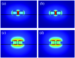
The structure of the slot waveguide with vertical sidewalls is shown in Fig. 1. A schematic of the slot with infinite height is shown in Fig. 1(a) and that of the slot with a finite height is shown in Fig. 1(b). Two Si strip waveguides with the same height (HSi) and width (WH) are separated by a slot on SOI with the width WS. The novel active material NaYF4:Er3+ NPs-PMMA covalently linked nanocomposites are chosen as the core layer. The α-NaYF4:10% Er3+ NPs are first synthesized using a mild hydrothermal method in a water–ethanol–OA mixed solvent system. The surface of NPs is modified by unsaturated functional groups, then copolymerized with methylmethacrylate (MMA). The NPs-PMMA covalently linked nanocomposites are synthesized and embedded into the slot by spin coating. Compared to the active material fabricated using physical doping, the higher concentration of the Er3+ dopant and the better stability are the prominent advantages of the present approach. The thickness of the active material is 3 μm. The modal profile should be simulated at both the signal wavelength λS (1530 nm) and the pump wavelength λP (1480 nm). The refractive index of the core is measured using the ellipsometry method (J. A. Woollam., Co. M 2000). The measured values of the core layer are 1.4853 and 1.4856 at 1530 and 1480 nm, respectively. The refractive indices of Si are 3.4779 and 3.482 at 1530 and 1480 nm, respectively. The refractive indices of SiO2 are 1.4442 and 1.4510 at 1530 and 1480 nm, respectively. When the Si strip waveguide with height HSi = 220 nm, width WH = 250 nm, and gap region width WS = 100 nm, the modal profiles and the effective refractive indices (Neff) of the slot waveguide under the condition of TE polarization are simulated at 1530 and 1480 nm, as depicted in Fig. 2(a) and (b), respectively. The optical field distributions of the slot waveguide under TM polarization in the pump light and signal light wavelengths are shown in Fig. 2(c) and (d).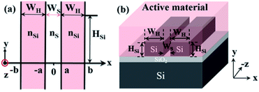 | ||
| Fig. 1 Schematic of slot waveguide. (a) Schematic of vertical slot with infinite height; (b) schematic of vertical slot with finite height. | ||
Optimization of slot waveguide combined with maximum power confinement in the slot
For a more intuitive view of the ability to confine the light field in the slot, we define the light field confinement factors (ΓS) in the slot region for TE and TM polarizations:28,29
 | (1) |
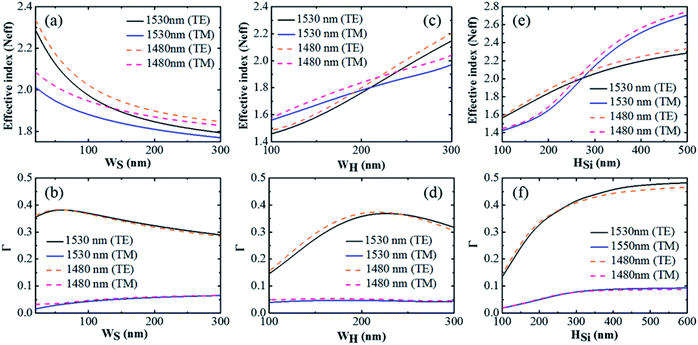
ΓS represents the effective utilization of energy, so we search for a maximum in all the considered cases, which could be used to achieve higher gain. The dependences of Neff and ΓS are simulated at 1530 nm and 1480 nm under TE and TM polarizations on WS for WH = 250 nm and HSi = 250 nm, as shown in Fig. 3(a) and (b). Neff decreases monotonically with increasing WS. Neff at 1480 nm was slightly larger than the Neff at 1530 nm. Neff under TE polarization is larger than that under TM polarization and as WS increased, the Neff under TE polarization decreased faster than that under TM. The confinement factor ΓS in the slot region at 1480 nm is essentially identical to the ΓS at 1530 nm and the ΓS under TE polarization is much higher than the ΓS under TM polarization. Apparently, the slot guiding structure supports a higher confinement in the slot region for the TE mode than for the TM mode. Both the pump and signal light are confined in the slot under TE polarization and their interaction is enhanced in the slot, which will be beneficial for achieving higher gain. Therefore, in this work, only the TE polarization mode is considered and the TM polarization mode is used for comparison only. Under TE polarization, ΓS first increases to the maximum value and then decreases, whereas under the TM mode, the ΓS increases slowly with increasing WS. Neff and ΓS show changes with different trends. For small WS, ΓS increases while Neff decreases because more light is confined in the low refractive index slot area. For WS increasing past maximum ΓS, more light will be limited to a low refractive index but not the slot area, with a majority of this light leaking into the cladding, leading to a decrease in both Neff and ΓS with increasing WS. As mentioned above, the electric field confined in the slot region was enhanced greatly due to the strong electric field coupling resonance at the two interfaces in the nanometer slot. Consequently, the advantage of the slot structure will not be significant with increasing WS and the high electric field intensity cannot be maintained. Similarly, Fig. 3(c) and (d) show Neff and ΓS as functions of WH. The Neff and ΓS values at 1480 nm are close to those at 1530 nm. Neff shows a constant linear increase with increasing WH. In contrast, ΓS first increases instantaneously to the maximum value and then decreases gradually. For small WH, two strip waveguides cannot confine the light slot and the silicon well, and more light leaks into the cladding. With increasing WH, the mode profile leaking into the cladding is gradually assigned to the silicon waveguide and the slot. The WH has an optimal value so that upon a further increase in WH, a fraction of light is distributed in silicon so that Neff increases while ΓS decreases. Since WH does not influence the cross-sectional area of the waveguide, a further increase in WH leads to a slow decrease in ΓS. The relationships of Neff and ΓS with HSi are shown in Fig. 3(e) and (f).
Optimization of slot waveguide combined with minimum effective mode area of the slot
Neff and ΓS increase monotonically with the increase in HSi. When HSi is relatively small, the mode profile at both ends of the slot area has a very high intensity and a majority of the light leaks into the cladding and the substrate. With the increase in HSi, the phenomenon of optical field leakage is alleviated. As the height continues to increase, the weak energy at the boundary is confined in the slot, so ΓS tends to saturate. However, an excessive HSi can lead to an increasing loss in the slot waveguide. To comprehensively consider the performance of erbium doped waveguide amplifiers (EDWA) based on the slot, the effective mode area (Aeff) is considered to optimize the size of the slot waveguide. We define Aeff as:30
 | (2) |
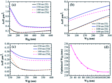
The EDWA based on the slot must have a small effective mode area conducive for achieving gain under low threshold power, where E(x,y) is the electric field in the entire cross-section of the waveguide. The Aeff values under TE and TM polarizations are plotted in Fig. 4 at 1530 nm and 1480 nm, respectively. As stated above, ΓS is predominantly affected by HSi. An increase in HSi of any amount can increase the ΓS value to some extent but a practical slot waveguide is formed with a finite height and an excessive height will give rise to superfluous transmission loss and coupling loss; we therefore carry out combined optimization of HSi and Aeff. Fig. 4(a) shows Aeff as a function of HSi at 1530 nm and 1480 nm under TE and TM polarizations, respectively, when WS is 100 nm and WH is 220 nm. The Aeff at 1480 nm is close to the Aeff value at 1530 nm and the Aeff value under TM polarization is greater than that under TE polarization. The slot under both polarizations has optimal values of HSi. Only the TE mode is considered because of its relatively weak ability to limit the light field and because of the larger Aeff in the TM mode. Then, the height of the slot was optimized for HSi = 250 nm. Fig. 4(b) shows the Aeff at 1530 nm and 1480 nm under TE and TM polarizations versus WS, respectively, when HSi is 250 nm and WH is 220 nm. Aeff increases monotonically as WS increases. Fig. 4(c) shows the Aeff at 1530 nm and 1480 nm under TE and TM polarizations for different WH (HSi = 250 nm, WS = 100 nm), respectively. The variation in Aeff for different WH is analogous to that versus HSi. For HSi = 250 nm, the optimized WH values for different WS values range between 220 nm and 230 nm, as shown in Fig. 4(d). A smaller Aeff is obtained for smaller WS. However, in actual experiments, polymers with small molecular weights can be filled into the narrow slot, while filling the active polymer with macromolecules is difficult. At present, a slot wider than 100 nm can be well filled. The filling ability of the active polymer can be improved by optimizing the diluent and viscosity. As shown in Fig. 3(b), the width of the slot with 100 nm is optimal and the corresponding optimal WH is 222 nm. The light field confinement factors (ΓS) in the slot region for TE polarization are 0.3805 and 0.3862 at 1530 and 1480 nm, respectively. The Aeff of 0.0806 μm2 and 0.0768 μm2 is obtained at 1530 and 1480 nm, respectively.
Gain characteristics of slot waveguide amplifier
Four-level spectroscopic model pumped at 1480 nm
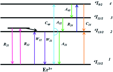
The Er3+-doped low refractive index material is filled into the slot waveguide and the potential gain of the slot waveguide amplifier is investigated. The gain characteristic analysis supported the optimization of the waveguide based on the Er3+-doped four-level system, as shown in Fig. 5 and pumping at 1480 nm was chosen owing to the excessive loss absorption at 980 nm in the silicon layers forming the slot waveguide.31 To achieve a more accurate simulation, the cooperative up-conversion (Cup), cross-relaxation (C14), and non-radiative decays (A43, A32) are involved. The operational principle of the amplifier pumped at 1480 nm is as follows: the Er3+ ions in the ground state absorb the pump energy and then transition from the 4I15/2 level to the higher Stark split sub-levels in the 4I13/2 excited level. Owing to thermal relaxation, Er3+ ions rapidly decay to the lower Stark split sub-levels in the 4I13/2 excited level and remain there longer. When the pump power exceeds the threshold power, population inversion occurs between 4I15/2 and 4I13/2. Then, the Er3+ ions in the 4I13/2 level transition down to the ground level 4I15/2 and emit the photons with the same frequency as that of the signal, so the device realizes the amplification function for the signal. Here, the amplified spontaneous emission (ASE) was neglected. Combined with the analysis of the energy level transitions for Er3+-doped four-level system, using the method of overlap integral, the simplified versions of the rate equations are obtained where N1, N2, N3, and N4 are defined as the concentrations of Er3+ in the 4I15/2, 4I13/2, 4I11/2, and 4I9/2 energy states, respectively. NEr is the total Er3+ ion concentration.Therefore, the rate equations were established and then solved using a formulized iteration method. The rate equations can be expressed by:
 | (3) |
 | (4) |
 | (5) |
 | (6) |
| N1 + N2 + N3 + N4 = NEr | (7) |
Then, the evolution of the signal and the pump power through the propagation length are described by:
 | (8) |
 | (9) |
σ12(vS) and σ21(vS) are the absorption and emission cross-sections of Er3+ for the signal, respectively, σ12(vP) and σ21(vP) are the absorption and emission cross-sections of Er3+ for the pump, respectively, and σ24(vP) is the excited state absorption of Er3+ for the pump. h is the Planck's constant, and αS and αP are the loss coefficients. Under steady-state conditions, the population densities maintain the dynamic balances considered in this system. Combining the signal and the pump propagation equations, the gain characteristics were analyzed using the Runge–Kutta method under the conditions of uniform doping and the steady state. The gain G was defined as follows:32
 | (10) |
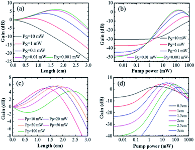
It is difficult to test all the parameters of the active polymer used in the simulation accurately. Incorporating the Judd–Ofelt theory, the absorption and emission spectrum are characterized, the parameter values of NaYF4:Er3+ NP-PMMA covalently linked nanocomposites are calculated as shown in Table 1. The maximum concentration of the Er3+ dopant of this novel material is 1.3 × 1027 m−3. The transmission loss of the slot waveguide filled with the active polymer measured by cutback method is about 9 dB cm−1. The set of atomic rate equations under the boundary conditions are solved using the formulated iteration method. The gain characteristics are obtained using the Runge–Kutta method combined with the propagation equations. First, the input signal power, pump power, and length of the slot waveguide are optimized by analysing the gain curves, as shown in Fig. 6.
| Symbol | Full name | Quantity |
|---|---|---|
| σ12P | Absorption cross section at 1480 nm | 7.53 × 10⁻²⁵ m2 |
| σ21P | Emission cross section at 1480 nm | 0.6 × 10⁻²⁵ m2 |
| σ24 | Excited state absorption cross section | 0.85 × 10⁻²⁵ m2 |
| σ12S | Absorption cross section at 1530 nm | 3.73 × 10⁻²⁵ m2 |
| σ21S | Emission cross section at 1530 nm | 8.62 × 10⁻²⁵ m2 |
| A21 | Spontaneous emission rate of N2 | 120 s−1 |
| A32 | Spontaneous emission rate of N3 | 1 × 10⁵ s−1 |
| A43 | Spontaneous emission rate of N4 | 1 × 10⁷ s−1 |
| Cup | Up-conversion coefficient | 3.2 × 10⁻²⁴ m3 s−1 |
| Loss_S | Transmission loss of the signal laser | 9 dB cm−1 |
| C14 | Cross-relaxation coefficient | 1 × 10⁻²³ m3 s−1 |
| Loss_P | Transmission loss of the pump laser | 9 dB cm−1 |
| NEr | Erbium ion density | 1.3 × 1027 m−3 |
| ΓS | Overlapping factor of the signal laser | 0.38 |
| ΓP | Overlapping factor of the pump laser | 0.386 |
| PP | Pump power | 400 mW |
For the pump power of 30 mW, the gain versus coordinate length of the slot waveguide for different signal powers is shown in Fig. 6(a). Fig. 6(b) indicates gain as the function of pump power at 1480 nm wavelength for different signal power with 1.5 cm slot waveguide. The effects of different input signal power intensities are shown and it can be seen that the gain increases gradually with decreasing signal power. When the signal power is 0.001 mW, the increase in the gain tends to be saturated. Small signal power is desirable and shows the dependence given by eqn (3). With the pump power increasing, the gain increases to the maximum value and then decreases. There is no saturated gain unlike for the pumping at 980 nm, which is mainly because the influence of the ESA occurs in the 4I13/2 level so that when the pump power exceeds the threshold power, the ions in the 4I13/2 level absorb the pump power and transition up, which decreases the impact on the gain. Therefore, the gain has shown the maximum value at the optimal pump power. Fig. 6(c) shows the gain versus the coordinate length of the slot waveguide for different pump power levels. With the input pump power increasing, the gain first increases gradually and then decreases continually, with the optimal pump power of approximately 20 mW. ESA is a detrimental process for amplifier gain and R24 of the material should be reduced. As can be seen, with the length of the slot waveguide increasing at different pump power levels, the gain first increases gradually and then decreases continually, and the length shows an optimum value. When the pump power increases, the gain corresponding to the optimal length also increases. This is because pump power is constantly consumed in the transmission along the waveguide, so after reaching the optimal waveguide length, the pump power is smaller than the threshold power and the amplification shuts off, with transmission loss causing negative gain when the length is too long. On increasing the input pump power, the pump power will reach the threshold power in the farther transmission direction. During this period, the device keeps amplifying the signal light so that the maximum gain is improved. Upon further increase in the pump power, ESA will decrease the gain. Fig. 6(d) shows the gain as a function of pump power at 1480 nm wavelength for different lengths of the slot waveguide for the signal power of 0.001 mW and pump power of 20 mW. The slot waveguide with 1.5 cm is required.
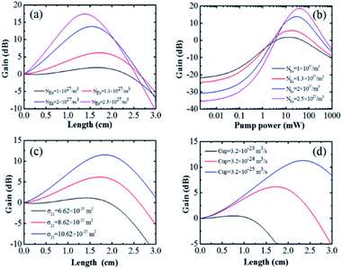
The concentration of Er3+ as a significant parameter directly impacts the gain. Fig. 7(a) shows the gain versus the coordinate length of the slot waveguide for different Er3+ concentrations. Fig. 7(b) shows the gain as a function of pump power at 1480 nm wavelength for different Er3+ concentrations. We can see that the higher the concentration of the material, the larger the gain. When the pump power is 20 mW, the gain increases with increasing Er3+ concentration and the optimal length decreases with it. When the length of the waveguide is 1.5 cm, the gain increases with increasing Er3+ concentration and the threshold pumping power also increases. This is because the threshold pumping power represents the minimum pump power for the occurrence of population inversion between the metastable energy level and the ground state energy level. Higher pump power is desired with increasing Er3+ concentrations. Then, a shorter length is needed for constant pump power. The Er3+ concentration of 1.3 × 1027 m−3 is chosen, the corresponding optimal length is approximately 1.5 cm, and the optimal pump power is 20 mW, both of which are in agreement with the values obtained by the above-described optimization. The higher Er3+ concentration is still expected and the novel active material NaYF4:Er3+ NP-PMMA allows the concentration of the Er3+ dopant an order of magnitude higher compared to the material obtained by physical doping, while the beneficial Er3+ concentration presents an interesting improvement in the synthesis of the active material. Fig. 7(c) shows the gain plotted versus the coordinate length of the slot waveguide for different signal emission cross-sections. The intensity of the signal emission cross-sections plays a highly important role in the amplification of signal light and for a small change in the emission cross-section of the signal photons, the gain could be highly depleted. In our work, the emission cross-section calculated by Judd–Ofelt theory is 8.62 × 10⁻²⁵ m2. The active material with larger emission cross-section is expected. Fig. 7(d) shows the gain as a function of pump power at 1480 nm wavelength for different up-conversion coefficients. The physical mechanism of the up-conversion is as follows: an excited ion in 4I13/2 gives its energy to another excited ion in the same state level and excites it to the higher energy level 4I19/2. A significant depopulation of the ions in 4I13/2 occurs, breaking the population inversion and reducing the gain. We can see from Fig. 7(d) that the gain decreases greatly with increasing up-conversion coefficient. The conversion coefficient is proportional to the Er3+ concentration. The doping of high Er3+ concentration will cause large conversion coefficient. When the pump power is constant, the optimal length decreases with increasing up-conversion coefficient. A homogeneous distribution of Er3+ can be useful in reducing the up-conversion.
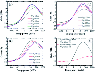
The gain versus coordinate pump power for different heights of silicon, widths of silicon, and widths of the slot were calculated using the optimized parameters, as shown in Fig. 8(a)–(c). When the width of silicon was 220 nm, the slot waveguide amplifier achieved the maximum gain. The height of the silicon was still the determining factor for the gain. Larger gain was achieved for greater height of silicon. The supererogatory transmission loss was not considered. A narrower slot is beneficial for acquiring larger gain with lower threshold pump power, while not considering the difficulty involved in the filling of the active material. The simulation results were consistent with the results of the above-described optimization. The slot waveguide amplifier achieved 5.78 dB net gain under TE polarization in a 1.5 cm waveguide when the height of silicon was 250 nm, the width of silicon was 220 nm, and the width of the slot was 100 nm. The propagation loss of the slot waveguide will be reduced by optimizing the fabrication technology and the net gain will be improved to a higher value.
Conclusions
In conclusion, NaYF4:Er3+ NPs-PMMA covalently linked nanocomposites were synthesized by copolymerization of NaYF4:Er3+ nanoparticles with methyl methacrylate. The stability and the concentration of the Er3+ dopant have been improved. This material was filled into the slot as the core layer. The full-vector finite difference method was demonstrated for the optimization of the slot waveguide by the precise analysis of power confinement and the minimum effective mode area of the slot. The modal characteristics under TE and TM polarizations were described. The slot guiding structure supported a higher TE mode confined in the slot region compared to the TM mode. When the slot waveguide had an optimal silicon height of 250 nm, a silicon width of 222 nm, and a slot width of 100 nm, the light field confinement factors (ΓS) in the slot region for TE polarization were 0.3805 and 0.3862 at 1530 and 1480 nm, respectively. The effective mode area (Aeff) values were 0.0806 μm2 and 0.0768 μm2 at 1530 and 1480 nm, respectively. A four-level spectroscopic model pumped at 1480 nm was presented. The rate equations and propagation equations were solved, and the gain characteristics of the slot waveguide amplifier were numerically simulated. The primary parameters were optimized. A net gain of 5.78 dB was achieved for the signal power of 0.001 mW at 1530 nm, pump power of 20 mW, Er3+ concentration of 1.3 × 1027 m−3, and waveguide length of 1.5 cm.Conflicts of interest
The authors declare no competing interests.Acknowledgements
This work was supported in part by the grant from the National Natural Science Foundation of China (NSFC) (61575078 and 61905088), Science and Technology Innovation Development Plan of Jilin City (201830793) and in part by Jilin Provincial Science and Technology Department (20190302014GX).Notes and references
- G. Stefano and M. Francesco, Nat. Commun., 2015, 6, 8182 CrossRef PubMed.
- A. Pospischil, M. Humer, M. M. Furchi, D. Bachmann, R. Guider, T. Fromherz and T. Mueller, Nat. Photonics, 2013, 7, 892–896 CrossRef CAS.
- A. Pospischil, M. Humer, M. M. Furchi, D. Bachmann, R. Guider, T. Fromherz and T. Mueller, Opt. Express, 2013, 21, 18236–18248 CrossRef PubMed.
- A. Biberman, M. J. Shaw, E. Timurdogan, J. B. Wright and M. R. Watts, Opt. Lett., 2012, 37, 4236 CrossRef CAS PubMed.
- R. Palmer, S. Koeber, D. L. Elder, M. Woessner, W. Heni, D. Korn, M. Lauermann, W. Bogaerts, L. Dalton, W. Freude, J. Leuthold and C. Koos, J. Lightwave Technol., 2014, 32, 2726–2734 CAS.
- E. Timurdogan, C. M. Sorace-Agaskar, J. Sun, E. Shah Hosseini, A. Biberman and M. R. Watts, Nat. Commun., 2014, 5, 4008 CrossRef CAS PubMed.
- Z. R. Tu, D. S. Gao, M. L. Zhang and D. M. Zhang, Opt. Express, 2017, 25, 20911–20922 CrossRef CAS PubMed.
- C. Caër, S. F. Serna-Otálvaro, W. W. Zhang, X. L. Roux and E. Cassan, Opt. Lett., 2014, 39, 5092–5794 CrossRef PubMed.
- D. Liang and J. E. Bowers, Nat. Photonics, 2010, 4, 511–517 CrossRef CAS.
- P. Pintus, S. Faralli and D. F. Pasquale, J. Lightwave Technol., 2011, 29, 1206–1212 CAS.
- E. D. Valdeiglesias, W. W. Zhang, A. Noury and C. A. Ramos, IEEE Trans. Nanotechnol., 2016, 15, 583–589 Search PubMed.
- A. R. Liu, H. S. Paniccia, M. Cohen and O. H. Dani, Opt. Express, 2004, 12, 4261 CrossRef PubMed.
- M. A. Foster, A. C. Turner, J. E. Sharping, B. S. Schmidt, M. Lipson and A. L. Gaeta, Nature, 2006, 441, 960–963 CrossRef CAS PubMed.
- M. L. Zhang, W. W. Zhang, F. Wang, D. S. Zhao, C. Y. Qu, X. B. Wang, Y. J. Yi, E. Cassan and D. M. Zhang, Sci. Rep., 2016, 6, 36729 CrossRef CAS PubMed.
- P. C. Zhao, M. L. Zhang, T. J. Wang, X. Y. Liu, X. S. Zhai, G. S. Qin, W. P. Qin, F. Wang and D. M. Zhang, J. Nanomater., 2014, 4, 153028 Search PubMed.
- S. Serna, P. Colman, W. W. Zhang, X. L. Roux, C. Caer, L. Vivien and E. Cassan, Sci. Rep., 2016, 6, 26956 CrossRef CAS PubMed.
- A. Spott, T. Baehr-Jones, R. Ding, Y. Liu, R. Bojko, T. O'Malley, A. Pomerene, C. Hill, W. Reinhardt and M. Hochberg, Opt. Express, 2011, 19, 10950–10958 CrossRef CAS PubMed.
- K. Debnath, A. Z. Khokhar, G. T. Reed and S. Saito, IEEE Trans. Nanotechnol., 2017, 29, 1269–1272 CAS.
- V. R. Almeida, Q. F. Xu, C. A. Barrios and M. Lipson, Opt. Lett., 2004, 29, 1209–1211 CrossRef PubMed.
- K. Gehlotand and A. Sharmal, Opt. Express, 2016, 24, 4722–4729 CrossRef PubMed.
- T. H. C. Hoang, W. W. Zhang, S. Serna, C. Caer, X. Le Roux, L. Vivien and E. Cassan, 17th International Conference on Transparent Optical Networks, 2015, vol. 1, pp. 1–4 Search PubMed.
- R. M. Guo, B. Wang, X. J. Wang, L. Wang, L. J. Jiang and Z. P. Zhou, Opt. Lett., 2012, 37, 1427–1429 CrossRef CAS PubMed.
- B. M. A. Rahman, IEEE Trans. Nanotechnol., 1995, 10, 187–216 Search PubMed.
- L. Liang, C. T. Zheng, Y. F. Yan, X. Q. Sun, F. Wang, C. S. Ma and D. M. Zhang, J. Mod. Opt., 2012, 59, 1084–1091 CrossRef CAS.
- D. M. Sullivan, Electromagnetic simulation using the FDTD method, John Wiley & Sons, 2013 Search PubMed.
- K. Bierwirth, N. Schulz and F. Arndt, IEEE Trans. Microwave Theory Tech., 1986, 34, 1104–1114 CrossRef.
- J. Xiao and X. Sun, Opt. Express, 2012, 20, 21583–21597 CrossRef PubMed.
- Y. J. Yi, H. R. Wang, Y. Liu and M. H. Jiang, IEEE Photonics Technol. Lett., 2015, 27, 2411–2413 CAS.
- S. A. Vázquez-Córdova, M. Dijkstra, E. H. Bernhardi, F. Ay, K. Worhoff, J. L. Herek, S. M. García-Blanco and M. Pollnau, Opt. Express, 2014, 22, 25993–26004 CrossRef PubMed.
- K. Saitoh, S. Makino, Y. Ishizaka, T. Fujisawa and K. Saitoh, J. Opt. Soc. Am. B, 2015, 32, 1245–1251 CrossRef.
- S. Serna, W. W. Zhang, X. Leroux, D. S. Gao, D. M. Zhang, L. Vivien and E. Cassan, J. Opt. Soc. Am. B, 2014, 31, 2021–2027 CrossRef CAS.
- G. F. R. Chen, X. Zhao, Y. Sun, C. He, M. C. Tan and D. T. H. Tan, Sci. Rep., 2017, 7, 3366 CrossRef PubMed.
| This journal is © The Royal Society of Chemistry 2020 |

