 Open Access Article
Electronic, magnetic and optical properties of MnPX3 (X = S, Se) monolayers with and without chalcogen defects: a first-principles study†
Juntao Yangab,
Yong Zhoua,
Qilin Guoa,
Yuriy Dedkov *a and
Elena Voloshina
 *ac
*ac
aDepartment of Physics, Shanghai University, 99 Shangda Road, 200444 Shanghai, P. R. China. E-mail: dedkov@shu.edu.cn; voloshina@shu.edu.cn
bSchool of Science, Hubei University of Automotive Technology, 167 Checheng West Road, Shiyan City, 442002 Hubei, P. R. China
cInstitute of Physical and Organic Chemistry, Southern Federal University, 344090 Rostov on Don, Russia
First published on 2nd January 2020
Abstract
Based on density functional theory (DFT), we performed first-principles studies on the electronic structure, magnetic state and optical properties of two-dimensional (2D) transition-metal phosphorous trichalcogenides MnPX3 (X = S and Se). The calculated interlayer cleavage energies of the MnPX3 monolayers indicate the energetic possibility to be exfoliated from the bulk phase, with good dynamical stability confirmed by the absence of imaginary contributions in the phonon spectra. The MnPX3 monolayers are both Néel antiferromagnetic (AFM) semiconductors with direct band gaps falling into the visible optical spectrum. Magnetic interaction parameters were extracted within the Heisenberg model to investigate the origin of the AFM state. Three in-plane magnetic exchange parameters play an important role in the robust AFM configuration of Mn ions. The Néel temperatures (TN) were estimated by means of Monte Carlo simulations, obtaining theoretical TN values of 103 K and 80 K for 2D MnPS3 and MnPSe3, respectively. With high spin state Mn ions arranged in honeycomb lattices, the spin-degenerated band structures exhibit valley polarisation and were investigated in different biaxial in-plain strains, considering the spin-orbital coupling (SOC). 2D MnPX3 monolayers show excellent performance in terms of the optical properties, and the absorption spectra were discussed in detail to find the transition mechanism. Different amounts and configurations of chalcogen vacancies were introduced into the MnPX3 monolayers, and it was found that the electronic structures are heavily affected depending on the vacancy geometric structure, leading to different magnetic state and absorption spectra of defected MnPX3 systems.
1 Introduction
Two-dimensional (2D) van der Waals materials have been recently extensively explored,1–5 owing to their unique electronic structures and interesting physical and chemical properties, since the first experiments on the demonstration of the extraordinary transport properties of graphene.6,7 For several decades, the family of 2D crystals has grown considerably with new additions such as boron nitride (BN),8 black phosphorus (BP)9 and transition metal dichalcogenides (TMDs).10 Recently, a series of 2D transition metal trichalcogenides (TMTs) MPX3 (M = V, Cr, Mn, Fe, Co, Ni and Zn; X = Se and Se) has gained many investigations over their synthesis and optical and electrical properties connected with weak interlayer van der Waals interactions.11–17 Bulk 3D MPX3 compounds can be prepared via chemical vapour deposition (CVD)14 and chemical vapour transport (CVT)18 methods with high crystal quality. By mechanical exfoliation and chemical intercalation, the 2D monolayers of MPX3 can be obtained with intermediate band gaps ranging from 1.3 eV to 3.5 eV,18 making them the ideal candidates for exfoliated 2D magnets and indicating their enhanced light absorption efficiency.18,19 DFT calculations predict that 2D MPX3 monolayers exhibit a large variety of magnetic behaviours, including ferromagnetic (FM) metal, antiferromagnetic (AFM) semiconductors and nonmagnetic (NM) insulators or metals, which can be effectively modulated via doping or lattice strain effects.20 These various magnetic functionalities of 2D MPX3 can be employed for low dimensional spintronic and magnetoelectronic applications. The wide range of band gaps indicate that 2D MPX3 compounds can also be considered as promising candidates for optoelectronic and clean energy generation and related water splitting applications.21,22Among the 2D MPX3 family, AFM phase MnPX3 compounds are the most interesting and widely focused materials due to the prediction of some exciting properties, such as visible-light catalytic activity,23 the possibility of use in valleytronics,24 doping-induced half-metallicity,25 etc. Their magnetic structure and spin ordering and control through doping and strain effects have been theoretically investigated.25–27 Notably, considering the treatment of spin-orbital coupling, 2D MnPX3 monolayers have been predicted with a spontaneous valley polarisation with degenerate spins.24 The magnetic behaviour and valley polarisation of 2D MnPX3 monolayers can be controlled by transition metal substitutions and electronic coupling via heterostructures, resulting in FM, half-metallic and bipolar magnetic semiconductors.28–30 These strategies offers a practical avenue for exploring novel valleytronic devices which can be fabricated from 2D MnPX3 monolayers.
It is well know that defects (dopants, vacancies, interstitial atoms, etc.) play a significant role in tailoring of 2D materials and controllable modifications can lead to drastic changes of their electronic, magnetic, optical and transport properties. Although many density functional theory (DFT) calculations have been carried out on the electronic and magnetic properties, the optical properties of 2D MnPX3 and the influence of chalcogen vacancies in these materials has been rarely investigated. Herein, we present an explicit investigation of the electronic structure of MnPX3 monolayers in order to gain insight into the magnetic and optical properties in detail. The influence of chalcogen vacancies on the electronic structure and magnetic and optical properties are also systemically studied and discussed in this work.
2 Computational details
Spin-polarised DFT calculations based on plane-wave basis sets of 500 eV cutoff energy were performed with the Vienna ab initio simulation package (VASP).31–33 The Perdew–Burke–Ernzerhof (PBE) exchange–correlation functional34 was employed. The electron–ion interaction was described within the projector augmented wave (PAW) method35 with Mn (3p, 3d, 4s), P (3s, 3p), S (3s, 3p) and Se (4s, 4p) states treated as valence states. The Brillouin-zone integration was performed on Γ-centred symmetry reduced Monkhorst–Pack meshes using a Gaussian smearing with σ = 0.05 eV, except for the calculation of total energies and densities of states (DOSs). For those calculations, the tetrahedron method with Blöchl corrections36 was employed. The 12 × 12 × 4 and 24 × 24 × 1 k-meshes were used for the studies of bulk and monolayer MnPX3, respectively, and the 12 × 12 × 1 k-mesh was used for the 2 × 2 × 1 supercells consisting of 4-fold unit monolayers in case of vacancy studies. In the case of 2D MnPX3, to ensure decoupling between periodically repeated layers, a vacuum space of 20 Å was used. The convergence criteria for energy and force were set to 10−6 eV and 0.005 eV Å−1, respectively.The PBE + U scheme37 was adopted to properly describe the strongly correlated system of Mn 3d orbitals with the effective on-site Coulomb interaction parameter U = 5 eV.24,38 The HSE06 hybrid functional39 was also used for some systems with a 12 × 12 × 1 k-mesh in order to get more accurate band gaps. Dispersion interactions were considered adding a 1/r6 atom–atom term as parameterised by Grimme (“D2” parameterisation).40
The single layer lattice dynamical stability was determined using the first principles phonon calculations code PHONOPY41 applying the finite displacement method42 within PBE + U. These phonon calculations were performed in 4 × 4 × 1 supercells and very tight convergence criteria of 10−8 eV for energy and 0.1 meV Å−1 for force were used with a 6 × 6 × 1 k-mesh. Monte-Carlo simulations were performed within the Metropolis algorithm43 to estimate the TN value, using periodic boundary conditions with a series of superlattices containing different amounts of magnetic sites. The optical spectra were calculated from the frequency dependent dielectric matrix after the electronic ground state had been determined.44 The PYPROCAR code was used to plot the spin-textures.45 Crystal structures and charge densities were visualised by VESTA.46
3 Results and discussions
3.1 Electronic and magnetic structure of 3D MnPX3
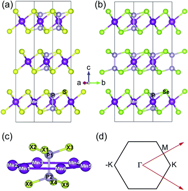
The three-dimensional (3D) bulk MnPS3 crystallises in the C2/m space group,47 while MnPSe3 in R![[3 with combining macron]](https://www.rsc.org/images/entities/char_0033_0304.gif) .48 Both of them can be represented in hexagonal unit cells as shown in Fig. 1(a) and (b), respectively (for details, see ESI,† Structural data for bulk MnPS3 and Structural data for bulk MnPSe3). Every unit cell contains three MnPX3 single layers which have D3d symmetry, despite the different 3D bulk space groups. The 2D MPX3 layer is composed of two Mn2+ ions which form a hexagonal honeycomb lattice and one [P2X6]4− bipyramid built from a P–P dimer connected with two sulphur/selenium trimers. The P–P dimer locates vertically across the centre of each honeycomb plane, with an in-plane twist of 60° between the top and bottom trimers as shown in Fig. 1(c). The lattice parameters a = b and c of 3D MnPX3 were fully relaxed in NM, FM and AFM magnetic states and they are listed in Table 1 with the respective total and relative energies. The energy difference ΔE = EAFM − EFM is −164 meV for 3D MnPS3 and −110 meV for 3D MnPSe3, demonstrating that MnPX3 bulk prefers the AFM state rather than the FM state. In particular, the NM states of 3D MnPX3 crystals show much higher energies than that of the AFM one (ΔE > 25 eV), revealing that the NM state is strongly unfavourable in energy. The AFM ground state lattice parameters are in a good agreement with the experimental values.47,48 Clearly, each lattice parameter and monolayer thickness d of MnPSe3 are larger than the corresponding values of MnPS3, caused by a larger ion radius of selenium compared to that of sulphur.
.48 Both of them can be represented in hexagonal unit cells as shown in Fig. 1(a) and (b), respectively (for details, see ESI,† Structural data for bulk MnPS3 and Structural data for bulk MnPSe3). Every unit cell contains three MnPX3 single layers which have D3d symmetry, despite the different 3D bulk space groups. The 2D MPX3 layer is composed of two Mn2+ ions which form a hexagonal honeycomb lattice and one [P2X6]4− bipyramid built from a P–P dimer connected with two sulphur/selenium trimers. The P–P dimer locates vertically across the centre of each honeycomb plane, with an in-plane twist of 60° between the top and bottom trimers as shown in Fig. 1(c). The lattice parameters a = b and c of 3D MnPX3 were fully relaxed in NM, FM and AFM magnetic states and they are listed in Table 1 with the respective total and relative energies. The energy difference ΔE = EAFM − EFM is −164 meV for 3D MnPS3 and −110 meV for 3D MnPSe3, demonstrating that MnPX3 bulk prefers the AFM state rather than the FM state. In particular, the NM states of 3D MnPX3 crystals show much higher energies than that of the AFM one (ΔE > 25 eV), revealing that the NM state is strongly unfavourable in energy. The AFM ground state lattice parameters are in a good agreement with the experimental values.47,48 Clearly, each lattice parameter and monolayer thickness d of MnPSe3 are larger than the corresponding values of MnPS3, caused by a larger ion radius of selenium compared to that of sulphur.
| X | State | ΔE | a | c | d | Mn–X | Mn–Mn |
|---|---|---|---|---|---|---|---|
| a Ref. 47.b Ref. 48. | |||||||
| S | NM | 25.582 | 5.789 | 18.991 | 3.065 | 2.44 | 3.34 |
| FM | 0.165 | 6.070 | 19.899 | 3.314 | 2.63 | 3.50 | |
| AFM | 0 | 6.064 | 19.893 | 3.313 | 2.62 | 3.51 | |
| Expta | 6.077 | 20.388 | |||||
| Se | NM | 26.201 | 6.144 | 19.286 | 3.379 | 2.56 | 3.55 |
| FM | 0.113 | 6.303 | 20.086 | 3.491 | 2.76 | 3.69 | |
| AFM | 0 | 6.398 | 20.082 | 3.487 | 2.76 | 3.69 | |
| Exptb | 6.387 | 19.996 | |||||
An interesting magnetic property for the bulk state is the interlayer magnetic coupling between monolayers in the unit cell. The energy differences between different inter-layer magnetic coupling ΔEint = EAFMint − EFMint are 0.5 meV and −0.27 meV for bulk MnPS3 and MnPSe3, respectively. Consequently, the FM inter-layer coupling is preferred for bulk MnPS3, but AFM is preferred for bulk MnPSe3. The different signs of ΔEint can be attributed to the different monolayer arrangement for the two bulks in different space groups. The small ΔEint is due to the large distance of about 7 Å between adjacent Mn honeycomb layers, and the neighbouring chalcogen atoms cannot act as a media bridge to mediate the long-range superexchange interactions across the large van der Waals gap, thus, the total energy is not sensitive to the inter-layer magnetic coupling, as in FePS3.49
Now the electronic structure of 3D MnPX3 is briefly discussed. The band structure and DOS obtained by the PBE + U method are shown in Fig. 2(a, b) and (c, d) for 3D MnPS3 and MnPSe3, respectively. The band structures are spin-degenerated in the AFM state, showing similar features for both bulk MnPX3 materials. The upper valence bands (VBs) at E − EF > −1.0 eV are mainly formed by S/Se p and partly by Mn 3d orbitals; the lower conduction bands (CBs), at E − EF < 3.5 eV for 3D MnPS3 and E − EF < 2.5 eV for MnPSe3, are mostly composed of S/Se p and the partial contributions from P p orbitals are almost equal to that of the Mn 3d states. The band gaps and the magnetic moments of Mn ions were extracted and are listed in Table 2. The GGA-PBE results give indirect band gaps of 1.31 eV for 3D MnPS3 and 1.08 eV for 3D MnPS3, respectively. As is well known, the GGA approximation usually underestimates the semiconductor band gap, thus, the PBE + U and HSE06 methods were further used to evaluate the band structure and resulting direct band gaps at the K point of the Brillouin Zone (BZ). The band gaps obtained by the PBE + U method are 2.37 eV for bulk MnPS3 and 1.81 eV for bulk MnPSe3. Moreover, the HSE06 functional predicts more accurate band gaps for the bulk systems with values of 3.08 eV and 2.50 eV for MnPS3 and MnPSe3, which shows good agreement with the experimental values of 3.0 eV and 2.5 eV,18 respectively. The magnetic moments of Mn ions calculated with the PBE + U method are 4.60 μB for both 3D MnPS3 and MnPSe3 (Table 2) and they are larger than that obtained with other functionals. These calculated values are in good agreement with the one obtained in the neutron diffraction experiments: 4.40 μB50 for MnPS3 and 4.74 μB48 for MnPSe3, revealing the high spin state of Mn2+ ions.
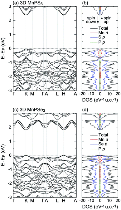 | ||
| Fig. 2 Band structures and total and partial DOS of (a and b) 3D MnPS3 and (c and d) 3D MnPSe3, obtained with PBE + U. | ||
3.2 Exfoliation energy and dynamical stability of 2D MnPX3
In order to evaluate the possibility of 2D MnPX3 monolayer mechanical exfoliation from the bulk, the cleavage energy was calculated by Ecl = (E(d0→∞) − E0)/A, where A is the in-plane area and d0 is the van der Waals gap of bulk crystals. The theoretical value of Ecl is 0.12 J m−2 for MnPS3 and 0.23 J m−2 for MnPSe3. The two Ecl values are smaller than the experimentally estimated cleavage energy in graphite (0.37 J m−2),51 indicating that the exfoliation of bulk MnPX3 is feasible in experiments. The Ecl = 0.23 J m−2 value for MnPSe3 is consistent with the previous theoretical results of 0.24 J m−2,52 whereas the Ecl = 0.12 J m−2 value for MnPS3 is much lower than the previous calculated value about of 0.26 J m−2.18 In other words, the Ecl value for MnPS3 is approximately twice smaller than the value calculated for MnPSe3 as can be explained by two factors. The dominant one is that the Se ions offer larger van der Waals force than the S ions, and it can be also confirmed by the comparison between the Ecl values for FePS3 (0.27 J m−2) and R![[3 with combining macron]](https://www.rsc.org/images/entities/char_0033_0304.gif) FePSe3 (0.38 J m−2).18 The second one is the different monolayer arrangement in the bulks between two bulk MnPX3 compounds and can be proved by the Ecl value of 0.16 J m−2 for fully relaxed MnPS3 in the R
FePSe3 (0.38 J m−2).18 The second one is the different monolayer arrangement in the bulks between two bulk MnPX3 compounds and can be proved by the Ecl value of 0.16 J m−2 for fully relaxed MnPS3 in the R![[3 with combining macron]](https://www.rsc.org/images/entities/char_0033_0304.gif) space group and 0.21 J m−2 for MnPSe3 in the C2/m space group.
space group and 0.21 J m−2 for MnPSe3 in the C2/m space group.
To estimate the dynamical stability of MnPX3 monolayers, the phonon spectra were calculated within the finite displacement method and the respective phonon dispersions are presented in Fig. 3 along the high-symmetry directions of the hexagonal BZ. Importantly, no imaginary modes in the phonon dispersions are observed, confirming the dynamical stability of 2D MnPX3, thus, they can be isolated in the experiments as freestanding layers. According to the phonon DOS given in right-hand side of the figure, the low frequency phonon bands below 8 THz for MnPX3 are dominated by Mn–S/Se interactions, whereas the middle and high frequency branches above 8 THz originate from the internal molecular vibrations of the [P2X6] group, consistent with the previous results.53 According to the fact that the radius and mass of selenium atoms are larger compared to that of sulphur, and that the bond length of Mn–Se is longer than that of Mn–S, the phonon bands of MnPSe3 are shifted to lower frequencies compared to those of MnPS3.
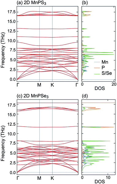 | ||
| Fig. 3 Phonon dispersion spectra and the corresponding DOS for (a and b) 2D MnPS3 and (c and d) 2D MnPSe3. | ||
3.3 Magnetic properties of 2D MnPX3
Four possible magnetic configurations were investigated to evaluate the ground state of 2D MnPX3 monolayers. The different spin configurations are FM, AFM-Néel, AFM-zig-zag and AFM-stripy (ESI, Fig. S1†). To extract the total energies of different magnetic structures, we used four ordered spin states defined using a 2 × 1 × 1 supercell. The total energies of different spin configurations and the relative energy differences with respect to the AFM-Néel configuration calculated within the PBE + U method are listed in Table 3. It can be seen that the lowest total energy is the AFM-Néel state for the 2D MnPX3 monolayer. In addition, NM configurations were also calculated, showing NM MnPX3 monolayers are in a semi-metallic state. Similar to that of 3D bulk unit systems, the NM state of 2D MnPX3 monolayers also shows much larger energies compared to the AFM ground state by 8.78 eV for MnPS3 and by 8.87 eV for MnPSe3, demonstrating that the MnPX3 monolayers persist with AFM magnetism similar to the 3D bulk system. Accordingly, the Mn ions magnetic moments of 2D MnPX3 are comparable to values for the 3D bulk state, listed in Table 2. Therefore one can conclude that 2D MnPX3 is a robust intrinsic AFM monolayer.To extract the exchange interaction parameters between Mn ions spins, the Heisenberg Hamiltonian was considered
 is the total spin magnetic moment of the atomic site and i, Jij are the exchange coupling parameters between two local spins. Considering one central Mn atom interacting with three nearest neighbouring (NN, J1), six next-nearest neighbouring (2NN, J2), and three third-nearest neighbouring (3NN, J3) Mn atoms. Here, the long-range magnetic exchange parameters (J) can be obtained by26
where S is the calculated magnetic moment of the Mn ion and EFM, EAFM-Néel, EAFM-zz and EAFM-str are the total energies in FM, AFM-Néel, AFM-zigzag and AFM-stripy magnetic configurations, respectively.
Using the presented results one gets J1 = 0.65 meV, J2 = 0.037 meV and J3 = 0.20 meV for 2D MnPS3 and J1 = 0.47 meV, J2 = 0.03 meV and J3 = 0.19 meV for 2D MnPSe3, which are in excellent agreement with the results from previous studies.26 With all positive exchange parameters J, these results indicate that both MnPS3 and MnPSe3 monolayers are in a robust AFM-Néel phase. The significant exchange interaction values indicate that the 2NN J2 and 3NN J3 exchange couplings make important contributions to the ground magnetic state, besides NN J1. The NN exchange J1 state comes from the competition between NN Mn–Mn direct exchange and Mn–X–Mn superexchange. The direct Mn–Mn interaction is always AFM according to the d orbital overlaps, while the Mn–X–Mn superexchange is always FM due to the Mn–X–Mn angle which is close to 90° (84.26° for MnPS3 and 84.03° for MnPSe3), as can be understandable from the well-known Goodenough–Kanamori–Anderson (GKA) rules.55–57 Because of the high spin Mn2+ d5 state and the short Mn–Mn distance (3.51 Å for MnPS3 and 3.69 Å for MnPSe3), the AFM direct exchange wins the competition and dominates the value of J1. The 2NN J2 and 3NN J3 exchange coupling parameters can be considered as super–superexchange interactions mediated by Mn–X⋯X–Mn bridges, and the strong hybridisation between X np orbitals and Mn 3d orbitals (see below) resulting in AFM interactions. According to the monolayer geometry, J3 involves a Mn–X1⋯X3–Mn bridge with two X ions located in the same chalcogen sub-layer and it is stronger than J2 with Mn–X1⋯X5–Mn with X ions located in separate sub-layers. In general, the AFM-Néel ground state is mostly from strong AFM direct exchanges between the Mn2+ ions for monolayer MnPX3.
On basis of the Ising model, Monte Carlo simulations with periodic boundary conditions were performed to estimate the Néel temperatures of MnPX3 monolayers. The three exchange parameters J1, J2 and J3 were used in a series of superlattices L × L (L = 16, 32, 64) containing a large amount of magnetic sites to accurately evaluate the value. Upon the heat capacity Cv(T) = (〈E2〉 − 〈E〉2)/kBT2 reaching the equilibrium state at a given temperature, the TN value can be extracted from the peak of the specific heat profile. The specific heat capacites per spin as a function of temperature are plotted in Fig. 4. From the simulated Cv(T) curves, one can find the peak ascent steepening as the lattice size increases. The accurately estimated TN value is 103 K for 2D MnPS3 and 80 K for 2D MnPSe3, which is in excellent agreement with the experimental values of 100 K (ref. 54) evaluated from the susceptibility data for MnPS3 and 74 K (ref. 48) revealed by neutron diffraction experiments for MnPSe3 in the bulk phase.
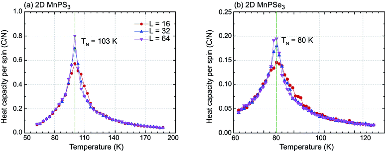 | ||
| Fig. 4 Specific heat capacity with respect to temperature for (a) 2D MnPS3 and (b) 2D MnPSe3 for different lattice sizes used in the Monte Carlo simulations. | ||
3.4 Electronic structures of 2D MnPX3
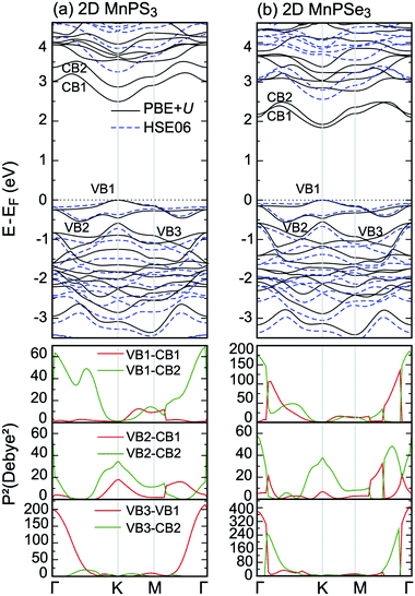
Having studied the magnetic ground state, the electronic properties of 2D MPX3 were investigated. The band structures calculated by PBE + U and the HSE06 method are presented in Fig. 5(a) and (b) for 2D MnPS3 and MnPSe3, respectively. As expected, both monolayers demonstrate semiconductor behaviour. The band gaps calculated by different functionals are given in Table 2. With a value of 3.25 eV for 2D MnPS3 and 2.56 eV for 2D MnPSe3 obtained by HSE06 functional, the gap is little larger than the corresponding value of the 3D bulk due to the quantum confinement effect when going from 3D to 2D. For 2D systems, the pure PBE functional gives direct band gaps at K point in a contrast to the other considered approaches (PBE + U and HSE06). As a consequence, 2D MPX3 can act as good candidates for 2D magnet semiconductors with a localised magnetic moment on the Mn ions.The upper VBs (above −0.5 eV) are composed of two bands, obtained by PBE + U, which almost overlap those of the HSE06 results. The other HSE06 VBs move towards a lower energy range compared to those of the PBE + U bands. One can see that the HSE06 CBs all move up to a higher energy range compared to that of the PBE + U bands, thus the HSE06 band gaps show the best consistency with the experimental values. However, the band dispersion of HSE06 is almost similar to that of PBE + U, that is to say, the main characters of the band structures are almost correctly described by the PBE + U method. Therefore, we focused on the total DOS and partial DOS of 2D MnPX3 obtained within the PBE + U method.
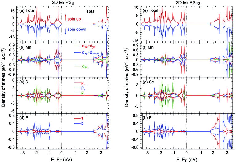
The total DOS and partial DOS are shown in Fig. 6: (a) for MnPS3 and (e) 2D MnPSe3, respectively. Due to the AFM ground state, the DOS is identical for spin up and spin down channels. Since the trigonal anti-prismatic MnX6 octahedron is under D3d symmetry in both monolayers, the Mn 3d orbitals can be decomposed into a single a1 (dz2) orbital and two 2-fold degenerate e1 (dxz, dyz) and e2 (dxy, dx2−y2) orbitals. The five d electrons occupy only one spin channel, leading to the high spin state of Mn ions, due to the strong crystal field effect. The top of the valence band VB is mainly dominated by the hybridisation between Mn d–e1, S/Se px and py orbitals, as shown in Fig. 6(b, c) and (f, g). Moreover, the strong hybridisation between Mn d–e1, e2 orbitals and S/Se px, py orbitals can be clearly seen in the whole energy range, confirming the superexchange interactions between the Mn d orbitals mediated by the S/Se p orbitals. The bottom of the conduction band CB is derived from Mn d–e1, e2, S/Se px, py and P p, s orbitals. Compared with that of 2D MnPS3, the contributions from the P s orbitals to the two lower CBs are stronger than those of P p states for 2D MnPSe3, as shown in Fig. 6(d) and (h), respectively. Clearly, a 0.25 eV sub-gap appears at 2.6 eV in CBs for MnPSe3 above the two lower CBs. In addition, from −0.5 eV to the Fermi level of the upper VBs, the hybridisation effect between Mn 3d and S p orbitals of 2D MnPS3, as reflected by one main sharp peak, is stronger than that of 2D MnPSe3 where two main sharp peaks are observed, resulting in more localised electron properties for MnPS3 than that for MnPSe3.
The different electronic structures of MnPX3 monolayers can be attributed to two factors: (i) the stronger crystal field effect in MnS6 octahedrons compared to that of MnSe6 due to the larger atomic radius and bond lengths of Se ions compared to those of S ions, as listed in Table 1; (ii) S ions have stronger electronegativity than Se ions, thus, the onsite energy of Se p and s orbitals is closer to that of Mn d states compared to the S ions. As a consequence, the d–p hybridisation in MnPS3 is stronger than that of MnPSe3, resulting in the larger band gap and more itinerant electrons of MnPS3 compared to those of MnPSe3. Moreover, the two factors can lead to stronger Mn–X⋯X–Mn mediated super–superexchange interactions in MnPS3 compared to those in MnPSe3, which can clarify that MnPS3 has higher a TN value than MnPSe3.
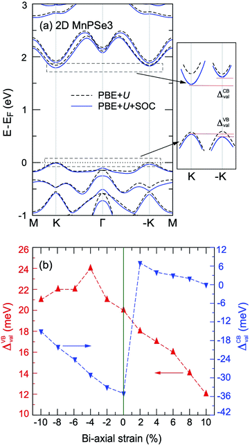
As a Néel AFM semiconductor is constructed with a honeycomb lattice, a spontaneous valley polarisation along with degenerate spins can be realised in 2D MnPX3 monolayers.24 In order to study the valley polarisation, 2D MnPX3 band structures were further investigated taking into account the spin-orbital coupling (SOC) (Fig. S2 in ESI†). The valley polarisation of 2D MnPSe3 is more significant than that of 2D MnPS3 (discussed below), herein we only present the band structure of the MnPSe3 monolayer with SOC taken into account (Fig. 7(a)). The respective valley polarisation can be estimated by the energy differences between the uppermost VB and lowest CB at the K and −K points of the BZ, defined as ΔCB/VBval = ECB/VBK − ECB/VB−K. The spontaneous valley degeneracy splittings of about ΔCB/VBval = 7/−3 meV for MnPS3 and 20/−35 meV for MnPSe3 appear for the uppermost VB band and lowest CB bands, respectively, which are consistent with previous studies.24,30 Due to the valley polarisation, the band gap slightly reduces to 2.49 eV for 2D MnPS3 and 1.80 eV for 2D MnPSe3, but remains direct at the K point. Caused by the SOC effect, the upper VBs show large energy-splittings of about 0.2 eV at the Γ point, compared to those of PBE + U bands, which demonstrate the twofold energy-degeneracy for the occupied VBs. Except for the Γ point, the SOC band dispersion shows similar features as that of PBE + U with small energy shifts along the high symmetry k-path. Due to the time-reversal symmetry, the total magnetic moments are 0 μB for any direction spin components for both 2D MnPX3 monolayers, as demonstrated by the SOC bands which do not show any spin-splitting in the momentum space.
Here, we also studied the effect of the biaxial in-plane strain in the MnPSe3 monolayer on the valley polarisation. The results of ΔVBval and ΔCBval with respect to the strain are plotted in Fig. 7(b) with positive and negative strains representing tensile and compressive effects, respectively. The tensile strain will enlarge the Mn–Mn bonds length while the compressive effect will enlarge the d–d direct AFM interactions. It is found that the tensile strains reduce valley polarisation ΔVBval, whereas the compressive strains slightly increase the value. For ΔCBval, both tensile and compressive strains reduce the absolute value, and interestingly the tensile strain will change the ΔCBval sign from negative to positive. As a result, the SOC band gap remains direct character under compressive strain but changes to indirect feature under tensile effect (uppermost VB at K point band and lowest CB at −K point). The strain effect to the band gap of SOC can be evaluated as ΔEg = Eg(K) − Eg(−K) = |ΔCBval| + |ΔVBval|. The estimated maximum value of ΔEg is 55 meV in the equilibrium state. That is to say, the valley polarisation of pristine MnPSe3 monolayers is most easily to be detected in experiment without in-plane strain which offers an undesirable influence on the valley polarisation.
3.5 Optical properties of 2D MnPX3
Besides the interesting magnetic properties, the 2D MnPX3 monolayers also show significant optical performance with band gaps in the fundamental range. The linear optical properties can be obtained from the frequency-dependent complex dielectric function as ε(ω) = ε1(ω) + iε2(ω), where ε1(ω) and ε2(ω) are the real and imaginary parts, respectively, of the dielectric function at the photon energy ω.44 To describe the decay of light intensity spreading in unit distance in medium, the absorption coefficient α(ω) can be calculated from the dielectric function as23,58Since the point group of the Néel AFM state is D3d, 2D MnPX3 monolayers process inversion symmetry which will introduce parity–forbidden transitions between VBs and CBs.59 In order to investigate the effect of symmetry-induced parity–forbidden transitions to the optical absorption properties, the transition dipole moment (TDM) defined by the electric dipole moment were calculated. For a single, non-relativistic particle of mass m, the TDM can be denoted in terms of the momentum operator p,60
It is well known that the optical properties strongly depend on the band structures. As mentioned above, the band structures obtained by the PBE + U method show the main features as those of the HSE06 functional. Herein, we paid our attentions to the optical properties of 2D MnPX3 evaluated by the PBE + U method. The lower panels of Fig. 5(a) and (b) show the curves for P2 with transitions from VB(1,2,3) to CB(1,2) (VB1 means the top VB and VB2 the second top VB, etc.; see upper panels of Fig. 5) along the high symmetry k-path according to the band structures. The absorption coefficient spectra α(ω) in a wide energy range are presented in Fig. 8 (a) for 2D MnPS3 and (b) for 2D MnPSe3.
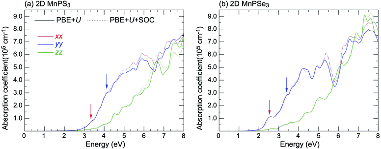 | ||
| Fig. 8 The absorption spectra of (a) 2D MnPS3 and (b) 2D MnPSe3 considered with and without a SOC effect within the PBE + U method. | ||
The curves of α(ω) for the two MnPX3 monolayers demonstrate some similar character in the whole energy range due to their similar band structures. All the spectra exhibit anisotropic character between in-plane xx (yy) components and out-plane zz components, corresponding to the 2D monolayer anisotropy. The threshold energy of the absorption spectra occurs at around 2.50 eV and 1.84 eV for 2D MnPS3 and 2D MnPSe3, respectively, according to their direct band gaps as fundamental absorption edge. However, the P2 spectra shows a zero value at the K point, it means a forbidden transition between the direct band edge. Additionally, the value of the P2 spectra between VB1 and CB1 is not very large, especially for 2D MnPS3, therefore, the absorption coefficient starts to increase very slowly at the fundamental band gap threshold. Nevertheless, with a higher energy phonon incidence, the α(ω) spectra increases sharply when the associated matrix elements are large and the transitions are allowed. For instance, around the Γ point, P2 spectra show the largest values for transitions from VB3 to VB1, and the α(ω) spectra increase rapidly around the corresponding energy of about 3.8 eV for 2D MnPS3 while a sharp peak at 2.6 eV for 2D MnPSe3 is shown. According to the different band gaps, it is evident that the P2 spectra of 2D MnPSe3 show much larger values than those of MnPS3 in the corresponding transitions and k points (Fig. 8). For example, with 3.2 eV photon induced, the absorption coefficient α(ω) shows a value of 2 × 105 cm−1 for 2D MnPSe3, which is four times larger than 0.5 × 105 cm−1 for 2D MnPS3. As a consequence, the 2D MnPSe3 monolayer is a stronger absorption efficiency material than 2D MnPS3, especially in the fundamental optical range.
The α(ω) spectra of these two compounds were further calculated taking into account SOC (see Fig. 8) and the obtained curves demonstrate the similar features as the spectra calculated on the basis of the initial PBE + U approach. In the low energy range under ∼5.0 eV, the absorption spectra calculated with PBE + U + SOC and PBE + U almost overlap each other, while showing some difference above ∼5.0 eV. Noticeably, the peaks marked by red and blue arrows at 2.6 eV and 3.4 eV reduce apparently with comparison to the PBE + U spectra for MnPSe3 SOC-α(ω), this is owing to the large energy-splitting for the SOC-VBs at the Γ point, leading to the descending of transition probabilities. Accordingly, the SOC bands of 2D MnPS3 do not show apparent energy-splitting at the Γ point (Fig. 7 and ESI, Fig. S2†), and the peaks marked by arrows at 3.4 eV and 4.2 eV do not exhibit much difference between SOC-α(ω) and PBE + U-α(ω) spectra. In addition, the marked peak at 2.6 eV for 2D MnPSe3 can be attributed to the electron transitions between the two highest bands of VBs and two lowest bands of CBs, and it is followed by a down-step absorption caused by the 0.25 eV sub-gap between 2.5 eV and 2.75 eV in the CBs. Meanwhile, the marked peak at 3.4 eV is followed by an up-step for αxx(ω) of MnPS3, and it can be attributed to the low DOS for the unoccupied orbitals between 3.2 eV and 3.4 eV.
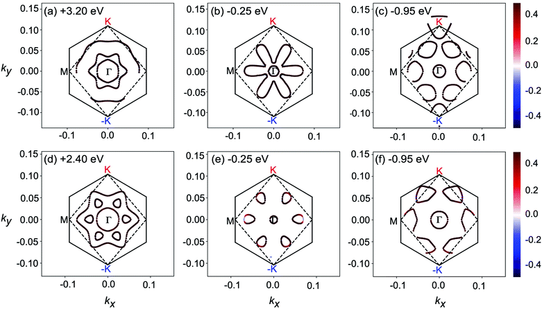
To further explore the underlying electron transition mechanism of 2D MnPX3, the kx–ky constant energy cuts of spin-textures were extracted from the calculated band structures as shown in Fig. 9 (the chosen energies for the cuts are marked for every panel and the energy differences between the low and high values are almost equal to the energy of the typical peaks in the absorption spectra mentioned above). All spin-textures are spin degenerated, caused by the robust intrinsic AFM state for both studied materials. Most importantly, the spin-textures show various circles, indicating the existence of electron pockets in the energy space for 2D MnPX3, which will benefit the electron transitions. For simplicity, we discussed the spin-textures of MnPSe3 monolayers to explore the transition possess. For 2D MnPSe3, the centre electron pocket at the Γ point belongs to VB1 at −0.25 eV, the six pockets located along the Γ–M path belong to VB2 at −0.25 eV and VB3 at −0.95 eV, whereas the empty pockets at +2.4 eV belong to both CB1 and CB2. Particularly, the six unoccupied pockets connected together as a whole big pocket for CB2. As shown in Fig. 5, the PVB2–CB22 spectrum exhibits a maximum peak at the Γ point, the PVB2–CB12 and PVB2–CB22 present some extreme values along the Γ–M path. Moreover, both PVB3–CB12 and PVB3–CB22 show much larger values along the Γ–M path. The combination of the abundant electron pockets and large value of P2 is advantageous to the electron transitions between the occupied VBs and empty CBs, leading to the marked peaks for the absorption coefficient of 2D MnPSe3 as discussed. According to the similar spin-textures, this mechanism can also be applied for the description of the electron transitions in 2D MnPS3. The optical absorption and electronic structures indicate that 2D MnPX3 monolayers would exhibit good performance for photocatalytic water splitting as shown in the previous study.23
3.6 Vacancy defects in 2D MnPX3
The effect of sulphur and selenium vacancies on the magnetic and optical properties of 2D MnPX3 is also investigated. In all considered vacancy systems, a 2 × 2 × 1 supercell was built to avoid the interaction between two defects or defect-pairs with the distance more than 10 Å. Three different amounts and geometric configurations of defects are discussed (Fig. 10): (a) one vacancy at the X1 site, named as VS@1L or VSe@1L with a defect concentration about 4.2%; (b) two neighbouring vacancies at sites X2 and X3 of the same chalcogen sub-layer named as VS2@1L or VSe2@1L with a concentration about 8.3%; (c) two neighbouring vacancies at sites X1 and X4 of different chalcogen sub-layers named VS2@2L or VSe2@2L (see Fig. 10(c)). The S/Se vacancy formation energy was calculated to evaluate the energetic stability:61 , where n is the defect number and Evac and EMnPX3 are the energies of relaxed vacancy system and pristine cell, respectively. The chemical potential energy is calculated from the most stable state of chalcogen crystal, as μS = −4.13 eV with the P2/c space group and μSe = −3.50 eV with the P21/c space group. The vacancy formation energies are presented in Table 4. All Ef values for S/Se vacancies are small, which implies easy defect formation in experiments. According to the different electronegativity of sulphur and selenium, it is found that Ef(VS) > Ef(VSe) in the corresponding systems, and Ef(VX2@1L) > Ef(VX2@2L) with the same defect account, revealing that the Se vacancy is more energetically favourable to produce than the S one, whereas a pair of vacancies is energetically unfavourable to produce in the same layer as VX2@1L rather than in the different layers as VX2@2L.
| Vacancy | Ef | MMn1/MMn6 | MMn2/MMn5 | MMn3/MMn4 | Ms/Mp/Md | Mtot | Eupg/Edowng |
|---|---|---|---|---|---|---|---|
| VS@1L | 1.41 | −4.584/4.583 | 4.583/−4.583 | −4.587/4.587 | −0.001/0.003/−0.001 | 0.001 | 2.39/2.38 |
| VS2@1L | 1.65 | −4.584/4.584 | 4.593/−4.592 | −4.587/4.586 | −0.001/0.003/0.000 | 0.002 | 1.62/1.63 |
| VS2@2L | 1.47 | −4.587/4.587 | 4.579/−4.579 | −4.587/4.587 | 0.000/0.000/0.000 | 0.000 | 2.26/2.26 |
| VSe@1L | 1.18 | −4.588/4.588 | 4.583/−4.583 | −4.588/4.587 | −0.001/0.003/−0.001 | 0.001 | 1.79/1.79 |
| VSe2@1L | 1.50 | −4.586/4.586 | 4.596/−4.595 | −4.593/4.592 | −0.001/0.003/0.000 | 0.002 | 1.26/1.26 |
| VSe2@2L | 1.26 | −4.593/4.593 | 4.579/−4.579 | −4.593/4.593 | 0.000/0.000/0.000 | 0.000 | 1.75/1.75 |
The magnetic moments M of different Mn ions, and total M of s, p or d orbitals are listed in Table 4 for 2D vacancy MnPX3 systems. Upon the vacancy defects induced, the 1X@1L and 2X@1L defect systems are all driven into a ferrimagnetic state with tiny net Mtotal values of about 0.001 μB and 0.002 μB, respectively, whereas the 2X@2L vacancy systems remain in an AFM state without a net magnetic moment. The different magnetic properties can result from the changed system symmetry of vacancy systems. All the vacancy systems have a bilateral-symmetry axis along the direction, while the 2X@2L system has one more inversion symmetry in the same direction. Accordingly, the Mn honeycomb lattice in a defect supercell shows some deformations with different M values for each Mn ion, as listed in Table 4. The total magnetic moments derived from different orbitals are also presented, and it should be noted that the net magnetic moment is dominated by the S/Se p orbitals around defects. However, with such a slight net Mtotal, the influence of chalcogen defects on the 2D MnPX3 monolayer can be almost neglected. In other words, the negligible Mtotal of vacancy MnPX3 further demonstrate the strong AFM interactions between the Mn ions in the honeycomb lattice.
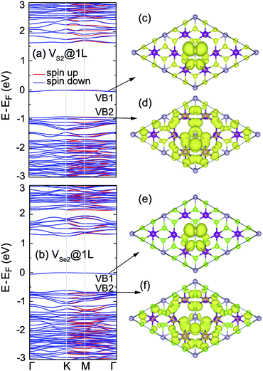
In order to seek the influence of chalcogen vacancies on the electronic properties of the 2D MnPX3, band structure, total and partial DOS of different defect-derived systems were then calculated (see ESI, Fig. S3†). According to the crystal symmetry change and net magnetic moment, the bands show a small spin-split along the K–M–Γ path, but remain spin degenerate along the Γ–K path for VX@1L and VX2@1L systems, while the band structures remain spin degenerate along the whole high-symmetry k-paths for VX2@2L systems. Strikingly, there is no isolated defect state generated within the band gap in the band structure for VX@1L and VX2@2L derived systems, but such a state appears in the band structure of the VX2@1L vacancy system (Fig. 11). These defect states appear as flat bands and they are mostly derived from the chalcogen and phosphorus p orbitals, as shown in the partial DOS. Herein, the partial charge density plots of VB1 and VB2 are illustrated in Fig. 11(c) and (d) for VS2@1L and Fig. 11(e) and (f) for VSe2@1L, respectively. As the chalcogen vacancy pair locates at X2 and X3 sites, the charge distribution mostly concentrates at neighbouring P1 and X1 ions, and partly at X5 and X6 sites for the mid-gap bands, all displaying p-like features, confirming the p orbital contribution to the defect state. For the VB2 states, the electron distributions locate at vacancy-neighbouring ions more than on the other ions, revealing that there are some defect states locating just under the Fermi level. Due to the defect states, the band gaps of vacancy systems are smaller than those of pristine monolayers, as listed in Table 4.
Without mid-gap bands generated, the uppermost VBs apparently show some flat band behaviours for VX@1L and VX2@2L monolayers, as shown for their band structures (ESI, Fig. S3†). It also can be further confirmed by the partial electron distribution which localises around the vacancies (ESI, Fig. S4†). As a consequence, the defect states are mainly located just under the Fermi level for the vacancy MnPX3 system without a mid-gap state. From comparison, the defect states of the 2D MnPS3 vacancy monolayer are more localised than those of the corresponding 2D MnPSe3 monolayer. Due to the defect states, the band gaps of vacancy systems are smaller than those of pristine monolayers, as listed in Table 4.
Vacancy defects strongly influence the optical properties of the host material. Herein, the absorption spectra of defected MnPX3 monolayers were investigated and the xx components of α(ω) are plotted in Fig. 12. The α(ω)xx spectra of vacancy systems show similar characteristics compared to those of pristine monolayers in the whole energy range except for the new defect-related peaks. The extreme values of absorption spectra alternate between the different systems with the continuous incident photon energy, revealing almost equal absorption efficiency for both pristine and defected systems. Some new features for the absorption spectra of vacancy systems should be noticed. Caused by the reduced band gaps, the α(ω) spectra threshold shifts to lower energy for the vacancy systems, compared with the α(ω)xx spectra of pristine monolayers. Particularly, a significant defect-peak appears at 1.70 eV for VS2@1L and 1.40 eV for VSe2@1L system, attributed to the direct transitions between the VB1 states to the lower part of the CBs of these n-type semiconductors. Similarly, the defect induced peaks in the energy range from 2.5 (2.0) eV to 3.0 (2.5) eV for MnPS3 (MnPSe3) vacancy systems also show significant width, although the defect states form flat bands under the Fermi level for VX@1L and VX2@2L systems. The SOC effect on the absorption spectra were also considered in the vacancy systems. For simplicity, only the xx component α(ω) spectra of VX2@1L systems are presented. As with that of pristine monolayers, the SOC-α(ω) spectra also show more smoothly than that of thr PBE + U-α(ω) spectra. Absorption spectra usually can be used as criteria to assess the crystal quality of the monolayers. Here, only the VX2@1L vacancy can be easily assessed with a new peak within the band gap for the absorption spectra. In addition, both VX@1L and VX2@1L vacancies could be probed by circularly polarised light due to the spin-splittings, as determined by the different transition dipole moments which show large splits between the spin up and spin down channels (Fig. 13). However, the VX2@2L defects cannot be easily detected because of the absence of both in-gap absorption peak and spin-splittings. From the discussion above, some further theoretical and experimental studies on the chalcogen vacancy defects should be carried out, such as circular polarisation, bound exciton and net magnetic detection, to identify the defect states and influence on the optical and magnetic properties of 2D MnPX3 monolayers.
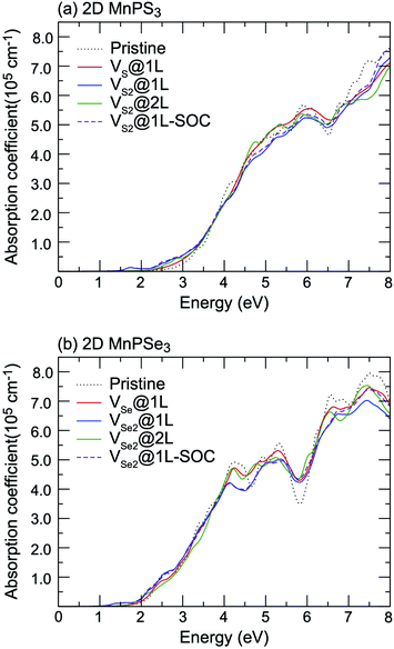 | ||
| Fig. 12 The xx component of the absorption coefficient α(ω) as a function of energy for pristine and defected (a) 2D MnPS3 and (b) 2D MnPSe3 systems. | ||
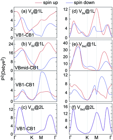 | ||
| Fig. 13 The square of transition dipole moment matrix for 2D MnPS3 (left panels) and 2D MnPSe3 (right panels) defected systems. | ||
4 Conclusions
A systematic first-principles study on the electronic, magnetic and optical properties of 2D transition-metal phosphorous trichalcogenide MnPX3 (X = S, Se) was carried out based on density functional theory. The bulk MnPS3 in the C2/m space group and MnPSe3 in the R![[3 with combining macron]](https://www.rsc.org/images/entities/char_0033_0304.gif) space group show AFM semiconductor behaviour with a direct band gap. For both materials, the monolayer form is energetically favourable and these layers can be exfoliated from the bulk phase with small cleavage energies, 0.12 J m−2 for MnPS3 and 0.23 J m−2 for MnPSe3, which are much lower than the 0.37 J m−2 of graphite. Confirmed by the phonon spectrum with no imaginary dispersion, MnPX3 monolayers show a good dynamical stability. The 2D MnPX3 monolayers are Néel AFM semiconductors with a direct band gap value of 2.37 eV (PBE + U) or 3.08 eV (HSE06) for 2D MnPS3 and 1.84 eV (PBE + U) or 2.56 eV (HSE06) for 2D MnPSe3 at the K point, in excellent agreement with the experimental data. The NN, 2NN and 3NN exchange parameters are all positive, revealing the AFM-Néel ground state of 2D MnPX3. Using periodic boundary conditions, Monte Carlo simulations gave theoretical TN values of 103 K and 80 K for 2D MnPS3 and MnPSe3, respectively. With high spin state Mn ions arranged in a honeycomb lattice, 2D MnPX3 shows valley polarisation with spin-degeneracy in the band structure if the spin-orbital coupling is considered. Moreover, in-plane strain offers an undesirable effect for the valley polarisation. With direct band gaps falling into the visible optical spectrum, MnPX3 monolayers have good performance for optical absorption which were investigated based on the electronic structures and transition dipole moment matrix. The influence of single and a pair of chalcogen vacancies on the electronic, magnetic and optical properties of MnPX3 were also investigated, and the effect is strongly correlated with the vacancy structure configurations. Two vacancies in the same chalcogen sublayer will introduce mid-gap state and spin-splitting, whereas two vacancies in different chalcogen sublayers show no mid-gap states and no spin-splitting. From the absorption spectra of vacancy systems, it is proposed that optical absorption spectra cannot be used as an ideal criteria to determine the crystal quality of the 2D MnPX3 monolayers.
space group show AFM semiconductor behaviour with a direct band gap. For both materials, the monolayer form is energetically favourable and these layers can be exfoliated from the bulk phase with small cleavage energies, 0.12 J m−2 for MnPS3 and 0.23 J m−2 for MnPSe3, which are much lower than the 0.37 J m−2 of graphite. Confirmed by the phonon spectrum with no imaginary dispersion, MnPX3 monolayers show a good dynamical stability. The 2D MnPX3 monolayers are Néel AFM semiconductors with a direct band gap value of 2.37 eV (PBE + U) or 3.08 eV (HSE06) for 2D MnPS3 and 1.84 eV (PBE + U) or 2.56 eV (HSE06) for 2D MnPSe3 at the K point, in excellent agreement with the experimental data. The NN, 2NN and 3NN exchange parameters are all positive, revealing the AFM-Néel ground state of 2D MnPX3. Using periodic boundary conditions, Monte Carlo simulations gave theoretical TN values of 103 K and 80 K for 2D MnPS3 and MnPSe3, respectively. With high spin state Mn ions arranged in a honeycomb lattice, 2D MnPX3 shows valley polarisation with spin-degeneracy in the band structure if the spin-orbital coupling is considered. Moreover, in-plane strain offers an undesirable effect for the valley polarisation. With direct band gaps falling into the visible optical spectrum, MnPX3 monolayers have good performance for optical absorption which were investigated based on the electronic structures and transition dipole moment matrix. The influence of single and a pair of chalcogen vacancies on the electronic, magnetic and optical properties of MnPX3 were also investigated, and the effect is strongly correlated with the vacancy structure configurations. Two vacancies in the same chalcogen sublayer will introduce mid-gap state and spin-splitting, whereas two vacancies in different chalcogen sublayers show no mid-gap states and no spin-splitting. From the absorption spectra of vacancy systems, it is proposed that optical absorption spectra cannot be used as an ideal criteria to determine the crystal quality of the 2D MnPX3 monolayers.
Conflicts of interest
There are no conflicts to declare.Acknowledgements
This work was supported by the National Natural Science Foundation of China (Grant No. 21973059). Y. J. thanks the support from the Natural Science Foundation of Hubei Province (Grant No. 2018CFB724) and from the Education Department (Grant No. D20171803). E. V. thanks the support by the Ministry of Education and Science of Russian Federation within the framework of the State Assignment for Research, Grants no. 4.6759.2017/8.9.References
- A. Geim, Science, 2009, 324, 1530–1534 CrossRef CAS PubMed.
- S. Z. Butler, S. M. Hollen, L. Cao, Y. Cui, J. A. Gupta, H. R. Gutierrez, T. F. Heinz, S. S. Hong, J. Huang, A. F. Ismach, E. Johnston-Halperin, M. Kuno, V. V. Plashnitsa, R. D. Robinson, R. S. Ruoff, S. Salahuddin, J. Shan, L. Shi, M. G. Spencer, M. Terrones, W. Windl and J. E. Goldberger, ACS Nano, 2013, 7, 2898–2926 CrossRef CAS PubMed.
- A. K. Geim and I. V. Grigorieva, Nature, 2014, 499, 419–425 CrossRef PubMed.
- G. R. Bhimanapati, Z. Lin, V. Meunier, Y. Jung, J. Cha, S. Das, D. Xiao, Y. Son, M. S. Strano, V. R. Cooper, L. Liang, S. G. Louie, E. Ringe, W. Zhou, S. S. Kim, R. R. Naik, B. G. Sumpter, H. Terrones, F. Xia, Y. Wang, J. Zhu, D. Akinwande, N. Alem, J. A. Schuller, R. E. Schaak, M. Terrones and J. A. Robinson, ACS Nano, 2015, 9, 11509–11539 CrossRef CAS PubMed.
- Z. Lin, Y. Lei, S. Subramanian, N. Briggs, Y. Wang, C.-L. Lo, E. Yalon, D. Lloyd, S. Wu, K. Koski, R. Clark, S. Das, R. M. Wallace, T. Kuech, J. S. Bunch, X. Li, Z. Chen, E. Pop, V. H. Crespi, J. A. Robinson and M. Terrones, APL Mater., 2018, 6, 080701–080721 CrossRef.
- A. K. Geim and K. S. Novoselov, Nat. Mater., 2007, 6, 183–191 CrossRef CAS PubMed.
- K. Novoselov, Rev. Mod. Phys., 2011, 83, 837–849 CrossRef CAS.
- K. Zhang, Y. Feng, F. Wang, Z. Yang and J. Wang, J. Mater. Chem. C, 2017, 5, 11992–12022 RSC.
- L. Li, Y. Yu, G. J. Ye, Q. Ge, X. Ou, H. Wu, D. Feng, X. H. Chen and Y. Zhang, Nat. Nanotechnol., 2014, 9, 372–377 CrossRef CAS PubMed.
- G. H. Han, D. L. Duong, D. H. Keum, S. J. Yun and Y. H. Lee, Chem. Rev., 2018, 118, 6297–6336 CrossRef CAS PubMed.
- C.-T. Kuo, M. Neumann, K. Balamurugan, H. J. Park, S. Kang, H. W. Shiu, J. H. Kang, B. H. Hong, M. Han, T. W. Noh and J.-G. Park, Sci. Rep., 2016, 6, 20904 CrossRef CAS PubMed.
- S. Lee, K.-Y. Choi, S. Lee, B. H. Park and J.-G. Park, APL Mater., 2016, 4, 086108 CrossRef.
- M. A. Susner, M. Chyasnavichyus, M. A. McGuire, P. Ganesh and P. Maksymovych, Adv. Mater., 2017, 29, 1602852 CrossRef PubMed.
- F. Wang, T. A. Shifa, P. Yu, P. He, Y. Liu, F. Wang, Z. Wang, X. Zhan, X. Lou, F. Xia and J. He, Adv. Funct. Mater., 2018, 28, 1802151 CrossRef.
- R. N. Jenjeti, R. Kumar, M. P. Austeria and S. Sampath, Sci. Rep., 2018, 8, 8586 CrossRef PubMed.
- S. Y. Kim, T. Y. Kim, L. J. Sandilands, S. Sinn, M.-C. Lee, J. Son, S. Lee, K.-Y. Choi, W. Kim, B.-G. Park, C. Jeon, H.-D. Kim, C.-H. Park, J.-G. Park, S. J. Moon and T. W. Noh, Phys. Rev. Lett., 2018, 120, 136402 CrossRef PubMed.
- R. Gusmão, Z. Sofer, D. Sedmidubský, S. Huber and M. Pumera, ACS Catal., 2017, 7, 8159–8170 CrossRef.
- K.-z. Du, X.-z. Wang, Y. Liu, P. Hu, M. I. B. Utama, C. K. Gan, Q. Xiong and C. Kloc, ACS Nano, 2016, 10, 1738–1743 CrossRef CAS PubMed.
- D. Mukherjee, P. M. Austeria and S. Sampath, ACS Energy Lett., 2016, 1, 367–372 CrossRef CAS.
- B. L. Chittari, Y. Park, D. Lee, M. Han, A. H. MacDonald, E. Hwang and J. Jung, Phys. Rev. B, 2016, 94, 184428 CrossRef.
- J. Chu, F. Wang, L. Yin, L. Lei, C. Yan, F. Wang, Y. Wen, Z. Wang, C. Jiang, L. Feng, J. Xiong, Y. Li and J. He, Adv. Funct. Mater., 2017, 27, 1701342 CrossRef.
- C.-F. Du, Q. Liang, R. Dangol, J. Zhao, H. Ren, S. Madhavi and Q. Yan, Nano-Micro Lett., 2018, 10, 67 CrossRef PubMed.
- X. Zhang, X. Zhao, D. Wu, Y. Jing and Z. Zhou, Adv. Sci., 2016, 3, 1600062 CrossRef PubMed.
- X. Li, T. Cao, Q. Niu, J. Shi and J. Feng, Proc. Natl. Acad. Sci. U. S. A., 2013, 110, 3738–3742 CrossRef CAS PubMed.
- X. Li, X. Wu and J. Yang, J. Am. Chem. Soc., 2014, 136, 11065–11069 CrossRef CAS PubMed.
- N. Sivadas, M. W. Daniels, R. H. Swendsen, S. Okamoto and D. Xiao, Phys. Rev. B: Condens. Matter Mater. Phys., 2015, 91, 235425 CrossRef.
- Q. Pei, X.-C. Wang, J.-J. Zou and W.-B. Mi, Front. Phys., 2018, 13, 666 Search PubMed.
- L. Zhong, X. Chen and J. Qi, Phys. Chem. Chem. Phys., 2017, 19, 15388–15393 RSC.
- Q. Pei, Y. Song, X. Wang, J. Zou and W. Mi, Sci. Rep., 2017, 7, 9504 CrossRef PubMed.
- Q. Pei and M. Wenbo, Phys. Rev. Appl., 2019, 11, 014011 CrossRef CAS.
- G. Kresse and J. Hafner, J. Phys.: Condens. Matter, 1994, 6, 8245–8257 CrossRef CAS.
- G. Kresse and J. Furthmuller, Comput. Mater. Sci., 1996, 6, 15–50 CrossRef CAS.
- G. Kresse and D. Joubert, Phys. Rev. B: Condens. Matter Mater. Phys., 1999, 59, 1758–1775 CrossRef CAS.
- J. Perdew, K. Burke and M. Ernzerhof, Phys. Rev. Lett., 1996, 77, 3865–3868 CrossRef CAS PubMed.
- P. E. Blöchl, Phys. Rev. B: Condens. Matter Mater. Phys., 1994, 50, 17953–17979 CrossRef PubMed.
- P. E. Blöchl, O. Jepsen and O. Andersen, Phys. Rev. B: Condens. Matter Mater. Phys., 1994, 49, 16223–16233 CrossRef PubMed.
- S. L. Dudarev, G. A. Botton, S. Y. Savrasov, C. J. Humphreys and A. P. Sutton, Phys. Rev. B: Condens. Matter Mater. Phys., 1998, 57, 1505–1509 CrossRef CAS.
- C. Franchini, R. Podloucky, J. Paier, M. Marsman and G. Kresse, Phys. Rev. B: Condens. Matter Mater. Phys., 2007, 75, 2573 CrossRef.
- J. Heyd, G. E. Scuseria and M. Ernzerhof, J. Chem. Phys., 2003, 118, 8207 CrossRef CAS.
- S. Grimme, J. Comput. Chem., 2006, 27, 1787–1799 CrossRef CAS PubMed.
- A. Togo and I. Tanaka, Scr. Mater., 2015, 108, 1–5 CrossRef CAS.
- S. Baroni, S. de Gironcoli, A. Dal Corso and P. Giannozzi, Rev. Mod. Phys., 2001, 73, 515–562 CrossRef CAS.
- N. Metropolis, A. W. Rosenbluth, M. N. Rosenbluth, A. H. Teller and E. Teller, J. Chem. Phys., 1953, 21, 1087–1092 CrossRef CAS.
- M. Gajdoš, K. Hummer, G. Kresse, J. Furthmuller and F. Bechstedt, Phys. Rev. B: Condens. Matter Mater. Phys., 2006, 73, 764 CrossRef.
- U. Herath, P. Tavadze, X. He, E. Bousquet, S. Singh, F. Muñoz and A. H. Romero, 2019, arXiv:1906.11387.
- K. Momma and F. Izumi, J. Appl. Crystallogr., 2011, 44, 1272–1276 CrossRef CAS.
- G. Ouvrard, R. Brec and J. Rouxel, Mater. Res. Bull., 1985, 20, 1181–1189 CrossRef CAS.
- A. Wiedenmann, J. Rossat-Mignod, A. Louisy, R. Brec and J. Rouxe, Solid State Commun., 1981, 40, 1067–1072 CrossRef CAS.
- X. Wang, K. Du, Y. Y. F. Liu, P. Hu, J. Zhang, Q. Zhang, M. H. S. Owen, X. Lu, C. K. Gan, P. Sengupta, C. Kloc and Q. Xiong, 2D Materials, 2016, 3, 1–9 CAS.
- K. Kurosawa, S. Saito and Y. Yamaguchi, J. Phys. Soc. Jpn., 1983, 52, 3919–3926 CrossRef CAS.
- R. Zacharia, H. Ulbricht and T. Hertel, Phys. Rev. B: Condens. Matter Mater. Phys., 2004, 69, 155406 CrossRef.
- X. Li, X. Wu and J. Yang, J. Am. Chem. Soc., 2014, 136, 11065–11069 CrossRef CAS PubMed.
- A. Hashemi, H.-P. Komsa, M. Puska and A. V. Krasheninnikov, J. Phys. Chem. C, 2017, 121, 27207–27217 CrossRef CAS.
- C. C. Mayorga-Martinez, Z. Sofer, D. Sedmidubský, Š. Huber, A. Y. S. Eng and M. Pumera, ACS Appl. Mater. Interfaces, 2017, 9, 12563–12573 CrossRef CAS PubMed.
- J. B. Goodenough, Phys. Rev. B: Condens. Matter Mater. Phys., 1955, 100, 564–573 CrossRef CAS.
- J. Kanamori, J. Appl. Phys., 1960, 31, S14–S23 CrossRef.
- P. W. Anderson, Phys. Rev., 1959, 115, 2–13 CrossRef CAS.
- V. Wang, W. Xiao, D. M. Ma, R. J. Liu and C. M. Yang, J. Appl. Phys., 2014, 115, 043708 CrossRef.
- W. Meng, X. Wang, Z. Xiao, J. Wang, D. B. Mitzi and Y. Yan, J. Phys. Chem. Lett., 2017, 8, 2999–3007 CrossRef CAS PubMed.
- V. Wang, N. Xu, J. C. Liu, G. Tang and W. T. Geng, 2019, arXiv:1908.08269.
- R. Ovcharenko, E. Voloshina and J. Sauer, Phys. Chem. Chem. Phys., 2016, 18, 25560–25568 RSC.
Footnote |
| † Electronic supplementary information (ESI) available. See DOI: 10.1039/c9ra09030d |
| This journal is © The Royal Society of Chemistry 2020 |

