
 Open Access Article
 This Open Access Article is licensed under a Creative Commons Attribution-Non Commercial 3.0 Unported Licence
Effects of substrates on proton irradiation damage of graphene
Weixin Wangab,
Shufen Wangac,
Siwei Zhanga,
Wei Wanga,
Xiang Ji *a and
Chunjing Li*a
*a and
Chunjing Li*a
aKey Laboratory of Neutronics and Radiation Safety, Institute of Nuclear Energy Safety Technology, Chinese Academy of Sciences, Hefei, Anhui 230031, China. E-mail: xiang.ji@fds.org.cn; chunjing.li@fds.org.cn; Tel: +86 551 6559-3681
bUniversity of Science and Technology of China, Hefei, Anhui 230026, China
cDepartment of Chemical and Materials Engineering, Hefei University, Hefei, 230601, China
First published on 25th March 2020
Abstract
In this paper, the irradiation damage of graphite sheets and monolayer graphene on Cu and Ni substrates after the proton irradiation with High Intensity D–T Fusion Neutron Generator (HINEG) were studied. The microstructure evolution of graphite sheets and monolayer graphene on different substrates was analyzed using Raman spectroscopy, X-ray photoelectron spectroscopy (XPS), and transmission electron microscopy (TEM). Results showed that the peak area ratio of carbon-oxides (C–O, C![[double bond, length as m-dash]](https://www.rsc.org/images/entities/char_e001.gif) O) in graphene was reduced after irradiation. 2–50 nm nanopores were produced in monolayer graphene on both Cu and Ni substrates. The results of Raman spectroscopy showed that the relationship between D and G peak intensity ratios (ID/IG) of irradiated graphene on diverse substrates was ID/IG(Cu) < ID/IG(Ni) < ID/IG(graphite), which indicated that the proton irradiation damage of graphene on the Cu substrate was the lightest. The reason for this could be speculated to be that different substrates had different damage self-repairing capabilities.
O) in graphene was reduced after irradiation. 2–50 nm nanopores were produced in monolayer graphene on both Cu and Ni substrates. The results of Raman spectroscopy showed that the relationship between D and G peak intensity ratios (ID/IG) of irradiated graphene on diverse substrates was ID/IG(Cu) < ID/IG(Ni) < ID/IG(graphite), which indicated that the proton irradiation damage of graphene on the Cu substrate was the lightest. The reason for this could be speculated to be that different substrates had different damage self-repairing capabilities.
1. Introduction
Graphene, two-dimensional (2D) carbon sheets arranged in a honeycomb lattice, is an outstanding material with various applications, due to its big theoretical specific surface area (2630 m2 g−1), high intrinsic mobility (200![[thin space (1/6-em)]](https://www.rsc.org/images/entities/char_2009.gif) 000 cm2 V−1 s−1), Young's modulus (∼1.0 TPa), thermal conductivity (∼5000 W m−1 K−1) and optical transmittance (∼97.7%).1–3 Nanoporous graphene (NPG), a kind of defective graphene with nano-scale pores on a two-dimensional base surface, is formed by removing the carbon atoms from the crystal lattice or transferring ones to the surface leaving a vacancy.4 The size of NPG can be grouped into micropores (<2 nm), mesopores (2–50 nm) and macropores (>50 nm).5 Therefore, compared to the inert perfect graphene surface, NPG not only retains the excellent properties, but its material transport efficiency also gets improved, especially for the separation of isotopes with little physicochemical difference. Lozada-Hidalgo et al.6 used the two-dimensional membranes of monolayer graphene to separate H+ from D+ successfully, with a separation factor up to 10 at room temperature. In addition, NPG has a pronounced application prospect in single-molecule sequencing, gas separation, seawater desalination, energy storage, and so on.
000 cm2 V−1 s−1), Young's modulus (∼1.0 TPa), thermal conductivity (∼5000 W m−1 K−1) and optical transmittance (∼97.7%).1–3 Nanoporous graphene (NPG), a kind of defective graphene with nano-scale pores on a two-dimensional base surface, is formed by removing the carbon atoms from the crystal lattice or transferring ones to the surface leaving a vacancy.4 The size of NPG can be grouped into micropores (<2 nm), mesopores (2–50 nm) and macropores (>50 nm).5 Therefore, compared to the inert perfect graphene surface, NPG not only retains the excellent properties, but its material transport efficiency also gets improved, especially for the separation of isotopes with little physicochemical difference. Lozada-Hidalgo et al.6 used the two-dimensional membranes of monolayer graphene to separate H+ from D+ successfully, with a separation factor up to 10 at room temperature. In addition, NPG has a pronounced application prospect in single-molecule sequencing, gas separation, seawater desalination, energy storage, and so on.
The research of NPG production mainly focuses on how to obtain high quality and high throughput array holes. Lots of techniques, like the mask-based lithography, chemical vapor deposition and particle beam irradiation, have been proposed in the recent years to produce NPG and control its structure. However, particle beam irradiation has higher energy transfer efficiency than mask-based lithography and chemical vapor deposition.7 The irradiation damages of graphene with particle beams had been widely carried out. Drndić et al.8 first fabricated nanometer-scale pores (∼3.5 nm) in multilayer graphene suspended on SiNx film under irradiation by transmission electron microscope (TEM) with the focused electron beam (200 kV). They got NPG with stable structures but have had no improvement so far. Similarly, scientists also studied the irradiation damage of graphene by other particle beams. For example, irradiation with Ar+, Ga+ and He2+ ion beams produced nanopores with diameters of 80 nm, 10 nm and 1.3 nm in graphene, respectively.9–11
In addition, some research studies on the irradiation damage of graphene by proton beams have also been reported. Ko et al.12 irradiated few-layer graphene on a SiO2/Si substrate by 5 MeV proton beams and found that high-energy proton irradiation could cause point defect damage in graphene. Mathew et al.13 studied the impact of the substrate and layer number on the stability of graphene by using 2 MeV proton beams to irradiate the graphene set in SiO2/Si substrate. The damage threshold of graphene samples was discovered to present a layer number-dependent effect and behave the same when using a substrate to support the graphene layer. Yang et al.14 researched the effect of doses on proton-irradiation damage of graphene by using various protons doses extending from 1 × 1016 cm−2 to 3 × 1016 cm−2 to irradiate monolayer graphene set in SiO2/Si substrate. The result showed that as the irradiation doses of proton beams increased, the monolayer graphene damages increased gradually. Lee15 and Zhang et al.16 both studied the effect of proton energy on damage formation in graphene by using protons with a different energy to irradiate monolayer graphene set in SiO2/Si substrate. They detected that the irradiation damage decreased as the proton energy increased. Combining experiments and simulations, they thought it was due to the low energy transfer of higher energy protons to graphene. Most of the current reports demonstrated the effects of graphene layer number, proton beam dose and energy on the irradiation damage of graphene on SiO2/Si substrates, while few have focused on the effect of substrates on proton irradiation damage of graphene. However, the researches of Compagnini et al.17 showed that when the graphene defect density was increased to exceed a certain threshold, the graphene ripples were suppressed intensely and the defective crystal adapted its shape to the substrate so as to maintain the thermodynamic stability. They also indicated that the reason of why monolayer graphene has a higher disorder than bilayer and multi-layer graphene is that they interact with the substrate differently. Therefore, it is quite necessary to explore the effects of substrates on proton irradiation damage of graphene.
In this paper, the effects of substrates on proton irradiation damage of graphene were investigated by proton beam irradiation. This work would play a crucial part in guiding the production of NPG through particle beam irradiation to graphene.
2. Experimental details
The Cu foil (100 × 100 mm), Cu and Ni substrates (Φ = 25 mm, d = 1 mm, purity: 99.99%) were all commercially obtained from Hefei Vigon Material Technology Co., Ltd (Hefei, China). The graphite sheets (Φ = 25 mm, d = 1 mm) were purchased from Dongteng Company. Poly (methyl methacrylate) (PMMA), chlorobenzene and acetone for the transfer of graphene were all purchased from Alfa Asha.The graphene was transferred from Cu foil to Cu and Ni substrates with the wet-transfer method as shown in Fig. 1. Firstly, graphene was grown on Cu foil through the technique of chemical vapor deposition (CVD). The graphene film grown on Cu foil has been analyzed with Raman spectra in Fig. 2. The results show that the intensity ratio of IG/I2D is lower than 1, and the 2D peak has a perfect single Lorentz peak type. It indicates that the prepared graphene is monolayer.13,16 Secondly, the graphene on Cu foil was spin-coated with a 6 wt% PMMA solution at 3600 rad s−1 and formed with a PMMA/graphene/Cu foil structure. Subsequently, we floated the PMMA/graphene/Cu foil structure on a Cu etchant (volume ratio of copper sulfate:hydrochloric acid:water = 1:5:5) for 30 min to form a PMMA/graphene structure. Then the PMMA/graphene structure was shifted onto a Cu or Ni substrate and the PMMA layer was removed by using acetone. Finally, the monolayer graphene/Cu and graphene/Ni substrate was prepared.
 | ||
| Fig. 1 The specific process of transferring the graphene on Cu foil to the Cu and Ni substrates by wet-transfer method. | ||
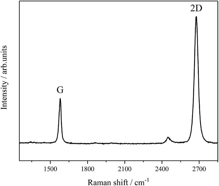 | ||
| Fig. 2 Raman spectra of the monolayer graphene film on Cu foil by CVD. | ||
As-prepared samples were irradiated with proton beam generated by a High Intensity D–T Fusion Neutron Generator (HINEG)18,19 under vacuum conditions. The parameters are shown in Table 1.
| Group | Ions energy (keV) | Beam intensity (mA) | Irradiation time (min) | Irradiation fluence (p cm−2) |
|---|---|---|---|---|
| A | 100 | 1 | 10 | 5.58 × 10¹⁶ |
| B | 250 | 1 | 10 | 5.58 × 10¹⁶ |
| C | 250 | 0.35 | 30 | 5.86 × 10¹⁶ |
Raman spectroscopy is an important method for quickly and non-destructively characterizing the crystal structure of graphene.20,21 The samples were measured by Raman spectra to investigate the disorder of the graphene. The samples were measured at room temperature with a Micro Raman spectrometer (Renishaw in Via Reflex, UK) of which the wavelength is 532 nm, the incident power is 5 mW (to avoid laser-induced heating and sample damage), and the spot size is about 2 μm. The C element's chemical states in samples were analyzed by Escalab 250Xi X-ray photoelectron spectroscopy (XPS) using the excitation source of Al-Kα. The binding energy of C element was determined at the pass energy of 100 eV, with an energy step of 1 eV. The Tecnai G2 F20 200 keV transmission electron microscope (TEM) has also been used as an indispensable instrument in the study of the structures of samples.
3. Results and discussions
3.1 Raman spectroscopy analysis
Due to the characteristic response to any variation in carbon hybridization state and defects or foreign species introduction, the Raman spectroscopy had been highly favored as the most important spectroscopic technique in studying the carbon-based materials all the time. Fig. 3 shows the development of Raman spectra of different samples non-irradiated and irradiated with the irradiation parameters of Group-A in Table 1. | ||
| Fig. 3 Raman spectra of different samples before and after irradiation. (a) Monolayer graphene on Cu substrate; (b) monolayer graphene on Ni substrate; (c) graphite sheets. | ||
Two typical characters of the monolayer graphene before irradiation are the G peak at 1580 cm−1 (with E2g symmetry, in-plane vibration of sp2 carbon atoms) and the 2D peak at 2690 cm−1 (two-phonon double-resonance Raman scattering process).20,21 The characteristics of pristine monolayer graphene used in the experiment are confirmed by three features: (1) the full-width-at-half-maximum (FWHM) of the 2D peak of graphene on Cu and Ni substrates are 34.8 cm−1 and 36.2 cm−1, respectively. (2) The intensity ratio of G peak and 2D peak of the graphene on Cu and Ni substrates are lower than 1. (3) The 2D peaks of the graphene on Cu and Ni substrates both have a perfect single Lorentz peak type.13,16,22,23 Also, the D peaks at ∼1350 cm−1 reflect that the presence of Raman active defects is weak enough to be ignored. There are also three characteristic peaks of D, G and 2D around 1350 cm−1, 1580 cm−1, and 2710 cm−1 in the graphite sheets. The graphite sheets could be considered as the multilayer graphene on graphite substrate due to a FWHM of ∼80.1 cm−1, IG/I2D > 1, and a 2D peak of a plurality of single Lorentz peak type. Meanwhile, the D peak of pristine graphite sheets is also very weak.
After the proton beam irradiation, the Raman spectra of different samples are all greatly changed. The 2D peaks are significantly broadened and their intensities are reduced so that they almost disappeared. The G peaks also appear to be significantly broadened, and their intensities are reduced to varying degrees. More importantly, for the disordered D peaks, their intensities are enhanced and their FWHM are also significantly increased. Therefore, a Raman spectrum similar to graphene oxide is formed because the D and the G peaks significantly overlap.24
It has been demonstrated that measuring the D peak intensity helps quantitatively analyze the defect density of graphene.25 The ratio of the intensity of the D–G peaks (ID/IG) is often used as an important parameter to characterize the defect density of graphene.21 Studies showed that the following relationship exists between ID/IG, the average distance between defects (LD), laser wavelength (λL, 532 nm) and defect density (nD).26
 | (1) |
 | (2) |
The calculation results are shown in Table 2. It could be seen that under the same irradiation condition, from the monolayer graphene on Cu substrate, the monolayer graphene on Ni substrate to the graphite sheets, the intensity ratio of D–G peaks (ID/IG) is sequentially increased, the average distance between defects (LD) is sequentially decreased, and the defect density (nD) is sequentially increased.
| Substrates | ID/IG | Average distance between defects LD (nm) | Defect density nD (cm−2) |
|---|---|---|---|
| Cu | 0.641 | 14.85 ± 2.10 | (1.44 ± 0.40) × 1011 |
| Ni | 0.914 | 12.44 ± 1.76 | (2.05 ± 0.57) × 1011 |
| Graphite | 0.967 | 12.09 ± 1.71 | (2.17 ± 0.60) × 1011 |
After irradiating graphene with proton beams of the same irradiation condition, what could be known from Table 2 is: ID/IG(Cu) < ID/IG(Ni) < ID/IG(graphite), LD(Cu) > LD(Ni) > LD(graphite), nD(Cu) < nD(Ni) < nD(graphite). It could be found that after the proton beam irradiation of graphene on different substrates under the same irradiation condition, graphene on different substrates have different irradiation damages: the monolayer graphene on the Cu substrate produces the least damage, the monolayer graphene on the Ni substrate produces the second damage, and the graphene on the graphite substrate (graphite sheets) produces the highest damage.
3.2 XPS analysis
As described in Section 3.1, the D peak and G peak of the graphene form a Raman spectrum similar to graphene oxidation. The C element's chemical states in samples unirradiated and irradiated are both dissected by XPS so as to check the oxidative degree of graphene. Fig. 4 shows the development of XPS spectra of the C 1s of different samples non-irradiated and irradiated by the parameters of Group-A in Table 1. | ||
| Fig. 4 XPS spectra of different samples' C 1s before and after irradiation (a) monolayer graphene on Cu substrate; (b) monolayer graphene on Ni substrate; (c) graphite sheets. | ||
The C 1s core peaks are divided into three symmetric Gaussian curves: a predominant sp2 C–C (binding energy EB = 284.6 eV), C–O (EB = 286.4 eV), CO (EB = 288.5 eV).27 As shown in Fig. 4(a)–(c), the peak area ratios of carbon-oxide-related (C–O and CO) are reduced from 25.16%, 33.78% and 29.81% to 19.67%, 32.34% and 28.42%, respectively. After proton beam irradiation, the peak area ratios of C–O and CO in graphene on Cu, Ni, and graphite substrates are reduced to different degrees, which are reduced by 5.49%, 1.44%, and 1.39%, respectively. During the irradiation process, the samples are all in a vacuum state and the peak area ratio of C–O and CO is low. There are two possible reasons for the reduction: (1) when graphene is bombarded by the proton beam, protons are combined with oxygen atoms to reduce carbon oxides. (2) The irradiation process raises the temperature of the graphene samples, boosting the thermal reduction of the carbon oxide. Therefore, the Raman spectrums are not formed by graphene oxide but by the damages of graphene after proton beam irradiation.
3.3 TEM analysis
According to the analysis in Section 3.1 and 3.2, after proton beam irradiation, damages are generated in graphene. The microscopic morphology of damages in graphene could be observed by TEM. After proton beam irradiation with the parameters of Group-A in Table 1, the monolayer graphene on Cu and Ni substrates were transferred to 200 mesh TEM copper grids by the wet-transfer method. Fig. 5 displays the microstructure of graphene after irradiation. | ||
| Fig. 5 TEM images of different samples after irradiation (a) monolayer graphene on Cu substrate; (b) monolayer graphene on Ni substrate. | ||
It could be seen from the TEM images that the nanopores (circled in red) are generated in the monolayer graphene on the Cu and the Ni substrates. In Fig. 5(a), a small number of nanopores (pore density: 1–3 nanopores/2.5 × 103 nm2) with similar pore sizes are observed in the monolayer graphene on Cu substrate. In Fig. 5(b), a large number of nanopores with higher pore density (pore density: 3–6 nanopores/2.5 × 103 nm2) with different pore sizes are observed in the monolayer graphene on Ni substrate. Pore density of the graphene on the Ni substrate is higher than that of the graphene on the Cu substrate, which is consistent with the difference of defect densities (nD(Ni) > nD(Cu)) in Table 2. Although the pore sizes of the nanopores produced in graphene on different substrates are different, their pore sizes are in the same range of 2–50 nm, which belong to mesopores.5
3.4 Reliability of experimental results
In order to verify the experimental data and the consistency of results, experiments under two other different irradiation conditions of Groups B and C of Table 1 were carried out. The samples before and after irradiation were also analyzed by Raman spectroscopy in Fig. 6. | ||
| Fig. 6 Raman spectra of different samples before and after irradiation (a) monolayer graphene on Cu substrate; (b) monolayer graphene on Ni substrate; (c) graphite sheets. | ||
After the proton beam irradiation with parameters of Group-B and Group-C in Table 1, the obvious Raman spectra changes of the graphene on different substrates are the same as that of Fig. 3. The 2D peaks of graphene on different substrates have been significantly broadened and their intensities are reduced. The G peaks also appear to be significantly broadened and their intensities are reduced to varying degrees. The intensities of the disordered D peaks are enhanced and their FWHM are significantly increased. The LD and nD were both calculated by formulas (1) and (2) and the calculation results are shown in Table 3.
| Group | Substrate | ID/IG | Average distance between defects LD (nm) | Defect density nD (cm−2) |
|---|---|---|---|---|
| B | Cu | 0.456 | 17.61 ± 2.49 | (1.02 ± 0.29) × 1011 |
| Ni | 0.755 | 13.68 ± 1.94 | (1.70 ± 0.47) × 1011 | |
| C | 0.942 | 12.25 ± 1.74 | (2.12 ± 0.59) × 1011 | |
| C | Cu | 0.679 | 14.43 ± 2.04 | (1.53 ± 0.42) × 1011 |
| Ni | 0.977 | 12.03 ± 1.70 | (2.20 ± 0.61) × 1011 | |
| C | 1.008 | 11.84 ± 1.68 | (2.27 ± 0.63) × 1011 |
Comparing results of Group-A in Table 2 with that of Group-B in Table 3, it could be found that for graphene on the same substrate (Cu or Ni or graphite), at the same beam intensity (1 mA), irradiation time (10 min) and irradiation fluence (5.58 × 10¹⁶ p cm−2), the greater the ions energy of the proton beam, the smaller the damages produced in graphene. This conclusion is consistent with the study of Zhang et al.16 Comparing results of Group-B with Group-C in Table 3, it could be found that for graphene on the same substrate (Cu or Ni or graphite), at the same ionic energy (250 keV), the damages of graphene are increased as the irradiation fluence increased and this conclusion is consistent with the study of Zeng et al.28 The above comparison of Group-A with Group-B and Group-B with Group-C shows that the data measured by Raman spectroscopy in three irradiation conditions is reliable. In Table 3, under different irradiation conditions of Group-B and Group-C, changes are the same for graphene on different substrates: ID/IG(Cu) < ID/IG(Ni) < ID/IG(graphite), LD(Cu)> LD(Ni) > LD(graphite), nD(Cu) < nD(Ni) < nD(graphite). The results show that different irradiation damages are produced in graphene on different substrates after proton beam irradiation under the same irradiation condition. The order of irradiation damage is: Cu < Ni < graphite. This conclusion is completely consistent with the conclusions obtained in Section 3.1.
3.5 Discussion
The reason of why graphene on different substrates has different damages after irradiation under the same proton irradiation condition may be that different substrates have different effects on self-repairing property of damages in graphene.The energy loss of protons in irradiated graphene was simulated by the particle transport software SRIM.29 The range of incident proton energy was designed varying from 10 keV to 10 MeV, and the carbon density was 1.8 g cm−3. The simulation results are shown in Fig. 7(a). The theoretical thickness of monolayer graphene is only 0.335 nm. It could be seen from the calculation that the energy loss of proton with 100 keV is about 44.25 eV and this energy is mainly transferred to the kinetic energy of the detached carbon ions. At the same time, the penetration depth of carbon ions in Cu, Ni and graphite were imitated by SRIM and the consequences are shown in Fig. 7(b). With the same incident energy of carbon ions, the immersion depth of carbon ions in graphite is the largest, while the depth in Cu and Ni are almost the same but smaller than that in graphite.
 | ||
| Fig. 7 Curve of SRIM simulation calculation. (a) Curve of energy loss proton in carbon material; (b) curve of projected range carbon ions in Cu, Ni and graphite. | ||
The microscopic process of irradiating the graphene on a substrate by proton beam is shown in Fig. 8. The carbon atoms in graphene are directly bombarded by proton beam to form detached carbon ions with a certain kinetic energy. Then the detached carbon ions are infiltrated into the substrate. The detached carbon ions in the substrate would be precipitated to the surface of the substrate due to their low solubility. Finally, the precipitated carbon ions are combined with the C atoms in the vicinity of the nanopores to form a C–C bond to repair the nanopores in graphene produced by the proton beam irradiation.
 | ||
| Fig. 8 Microscopic process figure of graphene on a substrate by proton beam irradiation. | ||
Under the same irradiation condition, the detached carbon ions produced by proton beam bombardment of graphene on different substrates have the same amount. Then, the detached carbon ions with a certain kinetic energy are permeated into Cu, Ni and graphite substrates at the same amount. The solubility of the detached carbon ions in Cu is much smaller than that in Ni and graphite.30,31 And the detached carbon ions penetrate almost the same depth in Cu and Ni, which is smaller than the penetration depth in graphite. The capability of the detached carbon ions to precipitate from the Cu substrate to its surface is the strongest due to the minimal carbon solubility and small penetration depth of Cu substrate. The capability of the detached carbon ions to precipitate from the graphite substrate to its surface is the weakest due to the maximal carbon solubility and the largest penetration depth of graphite substrate. The greater the capability of detached carbon ions to precipitate from the substrate to the surface, the more carbon ions are precipitated; the better the self-repairing property of damage in graphene, the smaller the damages are produced in graphene after proton beam irradiation.
The reason of why irradiation damages of graphene on different substrates are different after proton beam irradiation under the same irradiation conditions is that different substrates have different capabilities for the damage self-repairing in graphene. The greater the capabilities of different substrates, the smaller the damages of graphene are produced after irradiation. The capability from large to small is: Cu > Ni > graphite. Therefore, the damage of graphene on different substrates after irradiation from small to large is: Cu < Ni < graphite.
4. Conclusions
Proton beam irradiation has been used to introduce nanopores into graphene in the way of controllability. The joint use of Raman spectroscopy, XPS and TEM allow to verify the mechanisms of different damages formed in graphene on different substrates and to observe the microscopic morphology of damages. The defect densities (nD) of graphene on different substrates are nD(Cu) = (1.44 ± 0.40) × 1011 cm−2, nD(Ni) = (2.05 ± 0.57) × 1011 cm−2, nD(graphite) = (2.17 ± 0.60) × 1011 cm−2, respectively. It indicates that the graphene on the Cu substrate after proton beam irradiation suffered the least damages and the graphite sheets suffered the most. Different damages couldn't be completely ascribed to damages, stemming from the direct proton–C collisions. It's also because different substrates have different self-repairing capabilities of damages in graphene, which is demonstrated by the simulation results of SRIM and the different solubility of detached carbon ions in substrates. The self-repairing capability of damages in graphene of Cu substrate is the strongest among Cu, Ni and graphite. The graphite substrate has the weakest capability.Conflicts of interest
There are no conflicts to declare.Acknowledgements
This research was supported by grants from the National Natural Science Foundation of China (Grant No. 21773250 and 51802308). Thanks to the members of the FDS team for their help.References
- K. S. Novoselov, A. K. Geim, S. V. Morozov, D. Jiang, Y. Zhang and S. V. Dubonos, et al., Electric field effect in atomically thin carbon films, Science, 2004, 306(5696), 666–669 CrossRef CAS PubMed.
- A. K. Geim, Graphene: Status and Prospects, Science, 2009, 324(5934), 1530–1534 CrossRef CAS PubMed.
- T. S. Yang, H. Lin, X. R. Zheng, K. P. Loh and B. H. Jia, Tailoring pores in graphene-based materials: from generation to applications, J. Mater. Chem. A, 2017, 5(32), 16537–16558 RSC.
- S. Blankenburg, M. Bieri, R. Fasel, K. Mullen, C. A. Pignedoli and D. Passerone, Porous Graphene as an Atmospheric Nanofilter, Small, 2010, 6(20), 2266–2271 CrossRef CAS PubMed.
- M. E. Davis, Ordered porous materials for emerging applications, Nature, 2002, 417(6891), 813–821 CrossRef CAS PubMed.
- M. Lozada-Hidalgo, S. Hu, O. Marshall, A. Mishchenko, A. N. Grigorenko and R. A. W. Dryfe, et al., Sieving hydrogen isotopes through two-dimensional crystals, Science, 2016, 351(6268), 68–70 CrossRef CAS PubMed.
- X. Wu, F. Mu and H. Zhao, Synthesis and potential applications of nanoporous graphene: a review, Proceedings of the Nature Research Society, 2018, 2(02003), 1–13 CAS.
- M. D. Fischbein and M. Drndić, Electron beam nanosculpting of suspended graphene sheets, Appl. Phys. Lett., 2008, 93(11), 1–3 CrossRef.
- K. Tada, J. Haruyama, H. X. Yang, M. Chshiev, T. Matsui and H. Fukuyama, Graphene magnet realized by hydrogenated graphene nanopore arrays, Appl. Phys. Lett., 2011, 99(18), 1–3 CrossRef.
- D. Emmrich, A. Beyer, A. Nadzeyka, S. Bauerdick, J. C. Meyer and J. Kotakoski, et al., Nanopore fabrication and characterization by helium ion microscopy, Appl. Phys. Lett., 2016, 108(16), 1–4 CrossRef.
- A. Hemamouche, A. Morin, E. Bourhis, B. Toury, E. Tarnaud and J. Mathé, et al., FIB patterning of dielectric, metallized and graphene membranes: a comparative study, Microelectron. Eng., 2014, 121, 87–91 CrossRef CAS.
- G. Ko, H. Kim, F. Ren, S. J. Pearton and J. Kim, Electrical Characterization of 5 MeV Proton-Irradiated Few Layer Graphene, Electrochem. Solid-State Lett., 2010, 13(4), K32–K34 CrossRef CAS.
- S. Mathew, T. K. Chan, D. Zhan, K. Gopinadhan, A. R. Barman and M. B. H. Breese, et al., The effect of layer number and substrate on the stability of graphene under MeV proton beam irradiation, Carbon, 2011, 49(5), 1720–1726 CrossRef CAS.
- G. Yang, B. J. Kim, K. Kim, J. W. Han and J. Kim, Energy and dose dependence of proton-irradiation damage in graphene, RSC Adv., 2015, 5(40), 31861–31865 RSC.
- S. Lee, J. Seo, J. Hong, S. H. Park, J.-H. Lee and B.-W. Min, et al., Proton irradiation energy dependence of defect formation in graphene, Appl. Surf. Sci., 2015, 344, 52–56 CrossRef CAS.
- N. Zhang, X. Zhang, A. X. Yang, D. D. Ba, Z. Z. Feng and Y. F. Chen, et al., Damage effects of proton beam irradiation on single layer graphene, Acta Phys. Sin., 2017, 66(2), 297–301 Search PubMed.
- G. Compagnini, F. Giannazzo, S. Sonde, V. Raineri and E. Rimini, Ion irradiation and defect formation in single layer graphene, Carbon, 2009, 47(14), 3201–3207 CrossRef CAS.
- Y. Wu, Development of high intensity D-T fusion neutron generator HINEG, Int. J. Energy Res., 2018, 42(1), 68–72 CrossRef CAS.
- Y. Wu, C. Liu, G. Song, Y. Wang, T. Li and J. Jiang, et al., Development of High Intensity D-T fusion NEutron Generator (HINEG), EPJ Web Conf., 2017, 03006 CrossRef.
- A. C. Ferrari and J. Robertson, Interpretation of Raman spectra of disordered and amorphous carbon, Phys. Rev. B: Condens. Matter Mater. Phys., 2000, 20(61), 14095–14107 CrossRef.
- X. Q. Fan and L. P. Wang, Graphene with outstanding anti-irradiation capacity as multialkylated cyclopentanes additive toward space application, Sci. Rep., 2015, 5(1), 12734 CrossRef CAS PubMed.
- S. P. Surwade, S. N. Smirnov, I. V. Vlassiouk, R. R. Unocic, G. M. Veith and S. Dai, et al., Water desalination using nanoporous single-layer graphene, Nat. Nanotechnol., 2015, 10(5), 459–464 CrossRef CAS PubMed.
- Y. Zhu, D. K. James and J. M. Tour, New routes to graphene, graphene oxide and their related applications, Adv. Mater., 2012, 24(36), 4924–4955 CrossRef CAS PubMed.
- W. Z. Liang, X. Y. Chen, Y. Sa, Y. M. Feng, Y. Wang and W. Lin, Graphene oxide as a substrate for Raman enhancement, Appl. Phys. A: Mater. Sci. Process., 2012, 109(1), 81–85 CrossRef CAS.
- S. J. Zhao, J. M. Xue, Y. G. Wang and S. Yan, Effect of SiO2 substrate on the irradiation-assisted manipulation of supported graphene: a molecular dynamics study, Nanotechnology, 2012, 23(28), 285703–285710 CrossRef PubMed.
- L. G. Cancado, A. Jorio, E. H. M. Ferreira, F. Stavale, C. A. Achete and R. B. Capaz, et al., Quantifying Defects in Graphene via Raman Spectroscopy at Different Excitation Energies, Nano Lett., 2011, 11(8), 3190–3196 CrossRef CAS PubMed.
- L. P. Wang, X. Q. Fan, W. Li, H. Li, M. H. Zhu and J. B. Pu, et al., Space irradiation-induced damage to graphene films, Nanoscale, 2017, 9(35), 13079–13088 RSC.
- J. Zeng, J. Liu, H. J. Yao, P. F. Zhai, S. X. Zhang and H. Guo, et al., Comparative study of irradiation effects in graphite and graphene induced by swift heavy ions and highly charged ions, Carbon, 2016, 100, 16–26 CrossRef CAS.
- J. F. Ziegler, M. D. Ziegler and J. P. Biersack, SRIM - the stopping and range of ions in matter, Nucl. Instrum. Methods Phys. Res., Sect. B, 2010, 268(11–12), 1818–1823 CrossRef CAS.
- A. Cagliani, D. M. A. Mackenzie, L. K. Tschammer, F. Pizzocchero, K. Almdal and P. Boggild, Large-area nanopatterned graphene for ultrasensitive gas sensing, Nano Res., 2014, 7(5), 743–754 CrossRef CAS.
- Y. Zhu, S. Murali, W. Cai, X. Li, J. W. Suk and J. R. Potts, et al., Graphene and Graphene Oxide: Synthesis, Properties, and Applications, Adv. Mater., 2010, 22(46), 3906–3924 CrossRef CAS PubMed.
| This journal is © The Royal Society of Chemistry 2020 |