
 Open Access Article
 This Open Access Article is licensed under a Creative Commons Attribution-Non Commercial 3.0 Unported Licence
Minimising damage in high resolution scanning transmission electron microscope images of nanoscale structures and processes†
Daniel
Nicholls
 *a,
Juhan
Lee
ab,
Houari
Amari
ab,
Andrew J.
Stevens
cd,
B. Layla
Mehdi
abe and
Nigel D.
Browning
abce
*a,
Juhan
Lee
ab,
Houari
Amari
ab,
Andrew J.
Stevens
cd,
B. Layla
Mehdi
abe and
Nigel D.
Browning
abce
aDepartment of Mechanical, Materials and Aerospace Engineering and Department of Physics, University of Liverpool, Liverpool, L69 3GH, UK. E-mail: d.nicholls@liverpool.ac.uk
bThe Faraday Institution, Quad One, Harwell Science and Innovation Campus, Didcot OX11 0RA, UK
cSivananthan Laboratories, 590 Territorial Drive, Bolingbrook, IL 60440, USA
dOptimalSensing LLC, Southlake, TX 76092, USA
ePhysical and Computational Science Directorate, Pacific Northwest National Laboratory, Richland, WA 99352, USA
First published on 16th October 2020
Abstract
Beam damage caused during acquisition of the highest resolution images is the current limitation in the vast majority of experiments performed in a scanning transmission electron microscope (STEM). While the principles behind the processes of knock-on and radiolysis damage are well-known (as are other contributing effects, such as heat and electric fields), understanding how and especially when beam damage is distributed across the entire sample volume during an experiment has not been examined in detail. Here we use standard models for damage and diffusion to elucidate how beam damage spreads across the sample as a function of the microscope conditions to determine an “optimum” sampling approach that maximises the high-resolution information in any image acquisition. We find that the standard STEM approach of scanning an image sequentially accelerates damage because of increased overlap of diffusion processes. These regions of accelerated damage can be significantly decelerated by increasing the distance between the acquired pixels in the scan, forming a “spotscan” mode of acquisition. The optimum distance between these pixels can be broadly defined by the fundamental properties of each material, allowing experiments to be designed for specific beam sensitive materials. As an added bonus, if we use inpainting to reconstruct the sparse distribution of pixels in the image we can significantly increase the speed of the STEM process, allowing dynamic phenomena, and the onset of damage, to be studied directly.
The advent of aberration corrected STEM1 has led to an unprecedented increase in the achievable spatial resolution from all forms of imaging (Z-contrast, Annular Bright Field, etc.), but this has also been accompanied by a simultaneous increase in the operational probe current2 under typical imaging conditions. While the increased current is advantageous for observations of atomic scale dopants in some samples, typical electron doses are now several orders of magnitude higher than many materials can withstand.3 Dose considerations are now the most critical experimental parameters when imaging beam sensitive materials or performing in situ experiments, which usually leads to a reduction in the electron dose and dose rate4 at the cost of decreased signal-to-noise ratios and a poorer spatial resolution than the microscope is capable of delivering at the higher dose/rate levels. At the moment, determining the best dose/rate for any experiment is achieved through a trial and error approach, with the experimental microscopist balancing the imaging conditions to achieve an acceptable image/movie of the structure/process they are interested in. Such an approach depends critically on the expertise of the microscopist, and for any new sample or changed conditions, the expertise has to be established. However, it should be possible to define the optimum dose/rate that the specimen can survive based on our knowledge of the principle damage mechanisms that can take place. Our goal here is therefore to define the imaging conditions a priori for the highest spatial resolution images that can be achieved from any given sample or process while reducing the final beam damage to the specimen.
The two main damage types that samples experience in an electron microscope are knock-on5 (cascade displacement effects) and radiolysis6 (cleavage of chemical bonds) damage. These damage processes have sample and microscope parameter dependant critical thresholds7 – if the microscope parameters are maintained below this threshold (voltage, beam current, sample temperature) for a given sample, minimal damage will take place. To generalise these effects here we introduce the concept of beam influence (Fig. 1). Beam influence is the change in the sample that is a result of the beam-sample interactions, and similar to dose rate, beam damage will happen at a point in a sample when the beam influence exceeds a critical threshold. This allows us to discuss beam damage without needing the specifics of the underlying physical phenomena for each type of beam damage (for any given sample, the mechanism of damage will always be the same, the only difference will be how we put the beam into the specimen and the interactions that follow). For example, it has been shown that reducing the electron dose rate below a critical threshold causes the reduction of ceria by the electron beam to cease.8 This can be explained by a model that considers the influence of the beam on the sample to follow Fick's laws of diffusion. Beam influence imparted onto the specimen diffuses out from under the beam, and if the maximum beam influence accumulates and exceeds the critical threshold the sample becomes damaged.
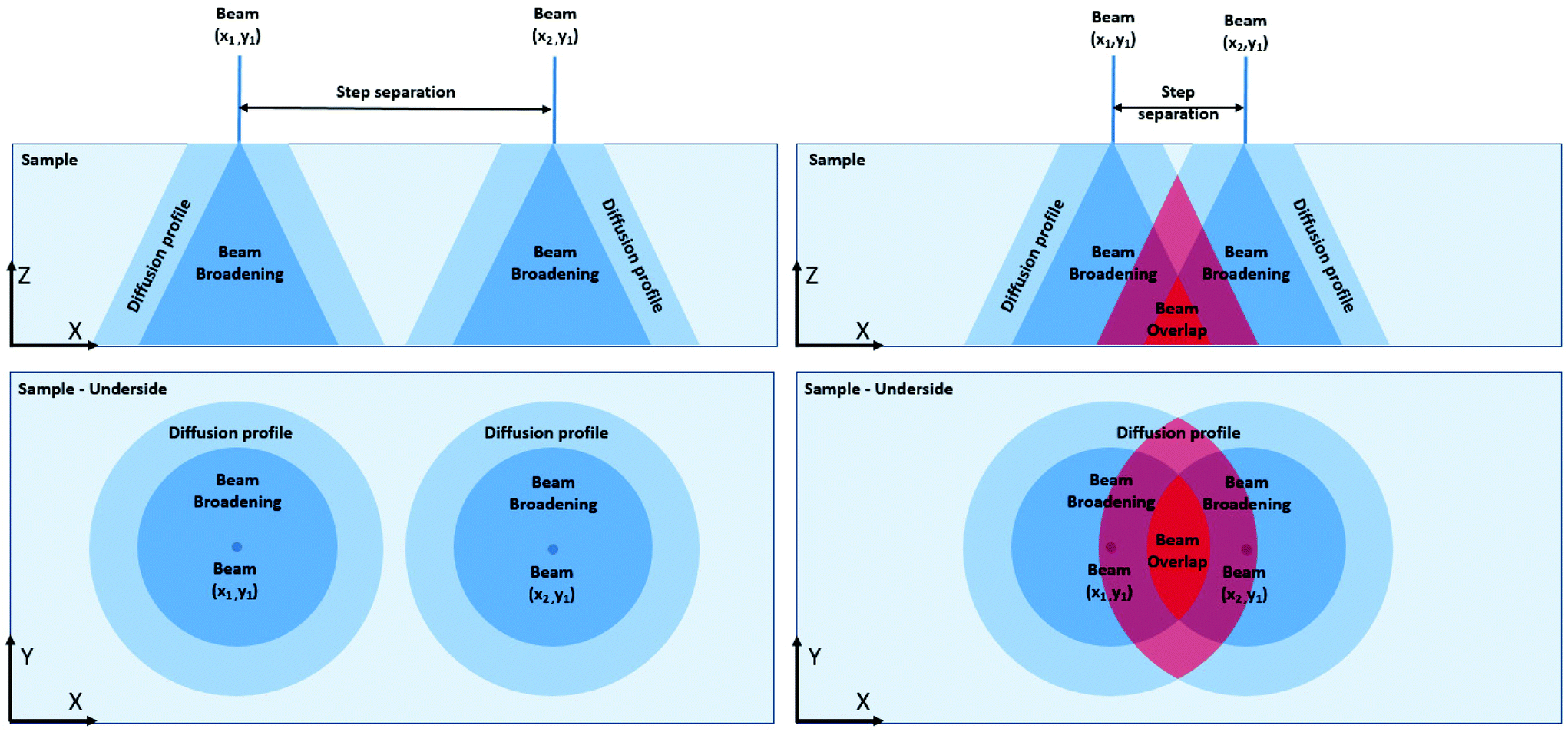 | ||
| Fig. 1 Small step separations between successive sampling points causes beam overlap due to beam broadening and/or diffusion effects (right). Increasing the step separation beyond a certain value reduces the effects of beam overlap (left). | ||
In using the concept of the beam influence, we can now examine how the delivery of the electron dose/rate to the sample affects damage. A simple example of this concept of beam influence is the difference between imaging a sample in either STEM or TEM mode. A TEM and a STEM experiment can have the same integrated dose and dose rate but the TEM mode illuminates a defined area for the entire image duration whereas the STEM mode illuminates smaller areas of the sample sequentially during the same acquisition time. In this example, the peak dose/rate in STEM is higher than for TEM, but the TEM area experiences the dose for a longer period of time and the influence of the beam on the sample will be different for each case. Here we will focus the discussion on the control of the beam influence in the STEM only (work defining the effects for TEM is ongoing). In typical STEM operation the electron beam performs a raster scan over the sample. At each position in the scan, beam influence is generated during the spot “dwell time” and the “diffusion time” of the interactions, increasing the beam influence beyond the area of the initial beam location and affecting neighbouring positions (Fig. 1). While individual scan positions may not produce enough beam influence to exceed the critical threshold, in a linear scan, every successive scan position may also experience “diffusion” interactions (Fig. 1, left). Furthermore, at the end of a line scan, when the beam returns to the left hand edge of the raster grid, the beam influence can further accumulate due to the beam influence generated from the previous line scan (the left hand edge of the STEM scan typically includes more damage as there is an extra stabilising dwell time after flyback). This phenomenon is effectively a diffusion profile overlap, and can affect the overall accumulated beam damage in three ways; point-to-point, line-to-line, and scan-to-scan. We note here that beam broadening in thick samples will exacerbate this effect, and for the remainder of this paper we will assume samples are of the same thickness or the thickness is normalised to the mean free path.9
Eqn (1) shows the change in beam influence per time step, the calculation of which is performed at every pixel in the system. The first term of the equation, D∇2φ, calculates the amount of beam influence that is diffusing, and the second term, f, is the amount of beam influence deposited at that pixel. The amount of beam influence that is deposited is determined by the probe location, which is generated via the scanning pattern, and beam broadening, which is governed by eqn (2). If the pixel is within the area of irradiation, beam influence is added
 | (1) |
 | (2) |
To investigate diffusion overlap independently from beam broadening a standard sample must be selected, and for this application a thin homogenous copper film was chosen. For the simulation, the material under consideration must have the following parameters defined; thickness, atomic number, lattice constant, and the number of atoms per unit cell. By choosing the thickness to be small, such that the thickness is much less than the mean free path, the beam broadening is negligible and the focus can be placed on the diffusion based phenomenon. Unless stated otherwise this copper film as described is used as standard, and changes to these parameters are mentioned explicitly.
As mentioned previously line hop sampling can be implemented to reduce the amount of line-to-line diffusion overlap, with the step separation being dictated by the lane width of the scan lines (how much the probe is allowed to vary perpendicular to the scan direction). The average step separation can then be controlled by the lane width, and therefore the amount of diffusion overlap that takes place. By sequentially increasing the lane width, and therefore the average step separation, the relationship between step separation and beam influence can be investigated for various microscope parameters.
Fig. 2 shows the evolution of the normalised maximum beam influence with regards to increasing step separation during line hop scanning. The maximum beam influence is defined as the maximum intensity value in the system throughout the entire time series, i.e. the most exposed position in the sample during scanning. Two parameters of interest are the dwell time, and the sample thickness, and the effects of varying these parameters can be seen in Fig. 2. Increasing either of these parameters increases the step separation necessary to reduce the maximum beam influence to a minimum. The reason for this is that these parameters cause the beam profile to grow larger, and thus the required step separation to reduce the overlap becomes larger as well. By normalising the maximum beam influence and the step separation by the beam influence intensity profile radius (FWTM) we can appreciate that the required step separation is dependent on the beam influence radius rather than just the dwell time or the sample thickness. For Fig. 2 a lapping scanning method was used to keep the beam dose and dose rate constant by increasing the number of laps as the sampling percentage goes down, i.e. performing 1 × 100% scan, 2 × 50% scans, 4 × 25% scans, etc. This approach shows that the reduction in maximum beam influence is due to the increased step separation and not the overall deposited electron dose.
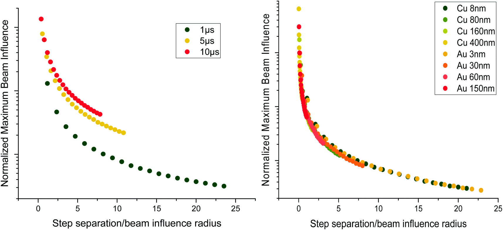 | ||
| Fig. 2 (a) Increasing dwell time causes an increase in the step separation required to avoid beam overlap in a thin sample. The reduction in beam influence is predominantly controlled by the step separation rather than the reduced dose. (b). Increasing sample thickness causes an increase in the step separation required to avoid beam overlap. In these plots, the separation of the beam is normalised by the beam profile radius, making the interpretation independent of instrument resolution. The beam influence is normalised to the effect of a single isolated beam location and is therefore plotted in arbitrary units. | ||
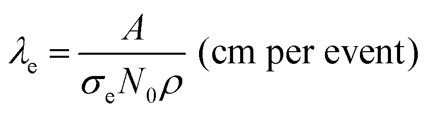
Fig. 2 shows the thickness dependence of the maximum beam influence during line hop scanning for two materials, a copper film and a gold film. The thickness values chosen for both the copper and gold films equate to T/λe = 0.1, 1, 2, and 5, with T as the sample thickness and λe being the mean free path of the electron for elastic scattering; λCu = 80 nm and λAu = 30 nm, calculated using;15
 | (3) |
 | (4) |
From Fig. 2 it can be seen that for a particular T/λe, regardless of elemental composition, the maximum beam influence at any given step separation is broadly equivalent. This is due to the fact that by setting  equivalent beam conditions have been introduced and therefore the beam radii are identical. The only difference between these two films at these conditions would be a change in the diffusion coefficient, which is not considered for this investigation into thickness effects. In this case, for simplicity, the beam is assumed to broaden uniformly through the sample, forming a pyramidal exposed area wherein the total deposited beam influence of each Z slice remains constant regardless of the beam radius.
Another parameter that affects the step separation which has been assumed up until this point is the diffusion coefficient of the beam influence. Beam influence is used in this study in order to generalise the damage mechanisms at play, and it can be considered that each mechanism of beam damage exists as a cross section of the beam influence, such that if a critical beam influence value is exceeded, then that damage type occurs. If we simplify the system and assume there is only one damage mechanism that occurs, such as vacancy migration, then this mechanism can be studied using this model, and the step separation required to minimise this phenomenon can be calculated, by setting the beam influence diffusion coefficient to the diffusion coefficient of the concerned phenomenon. In the more reasonable case that many phenomena occur then setting the beam influence diffusion rate to the quickest of the diffusing mechanisms would give the step separation required to produce the least damage overall – if overlap for a quick phenomenon is avoided, it must be avoided for slow phenomena as well. Fig. 3 shows the step separations required to minimise the maximum beam influence for a range of diffusion coefficients.
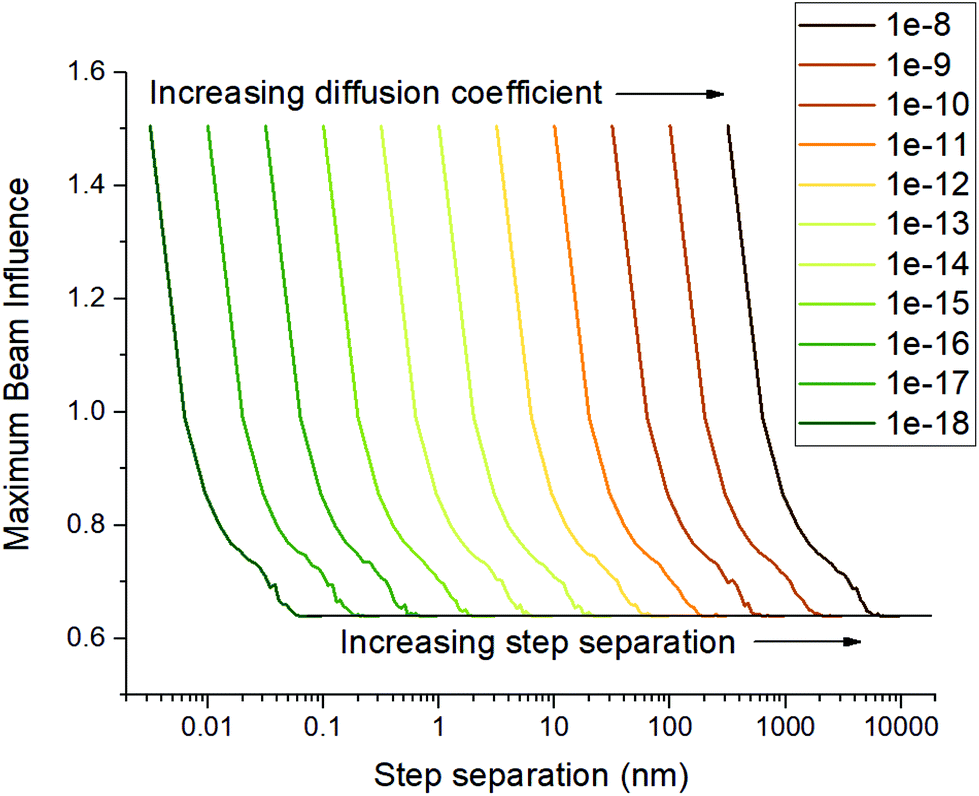 | ||
| Fig. 3 Increasing the diffusion coefficient increases the step separation required to minimise the maximum beam influence. The beam influence is normalised to the effect of a single isolated beam location and is therefore plotted in arbitrary units. | ||
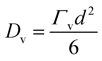
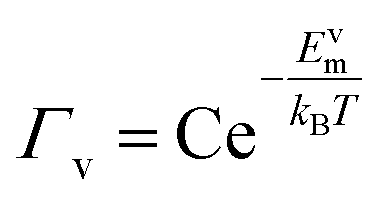
Following from the previous example, the diffusion coefficient of vacancy migration, Dv, can be calculated from;16
 | (5) |
 | (6) |
| Diffusion coefficients – E. L. Cussler | |||
|---|---|---|---|
| Solute | Solvent | T (°C) | D (m2 s−1) |
| Hydrogen | Water | 25 | 4.50 × 10⁻⁹ |
| Oxygen | Water | 25 | 2.10 × 10⁻⁹ |
| Ethanol | Water | 25 | 8.40 × 10⁻¹⁰ |
| Particle | Medium | T (°C) | D (m2 s−1) |
|---|---|---|---|
| Gold | Lead | 285 | 4.60 × 10⁻¹⁰ |
| Hydrogen | Iron | 100 | 1.24 × 10⁻¹¹ |
| Hydrogen | SiO2 | 500 | 1.30 × 10⁻¹² |
| Hydrogen | Iron | 10 | 1.66 × 10⁻¹³ |
| Hydrogen | SiO2 | 200 | 6.50 × 10⁻¹⁴ |
Clearly, distributing the dose in time and space is important, and by extension how that dose is distributed must be important as well. Besides raster and line hop sampling, 2D Bernoulli sampling can also be used to spatially distribute the electron beam dose. Fig. 4 features examples of line hop and random sampling schemes at a distribution of sampling percentages, and Fig. 4b shows how the sampling schemes in Fig. 4a change how the maximum beam influence and scan times vary. For Fig. 4b the scan time measurements do not take pixel to pixel travel time or flyback time into account. Fig. 4b shows how the average maximum beam influence decreases with sampling percentage, and notably at low sampling percentages, the line hop sampling that was used to overcome the hysteresis in the scan coils actually performs better than the purely random sampling.
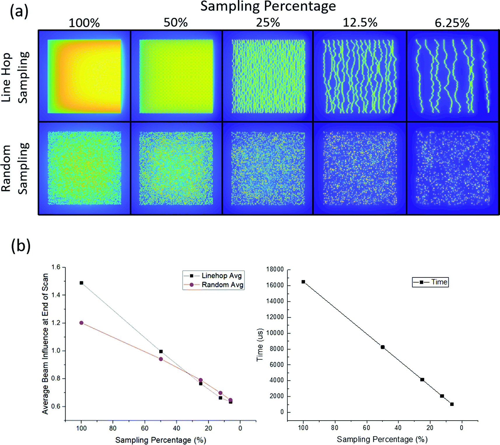 | ||
| Fig. 4 (a) Line hop sampling provides an approximately equivalent distribution to random sampling at the same sampling percentage. The irradiated area is 128 × 128 pixels. (b) (Left) Reducing sampling percentage reduces the beam influence for line hop and random scans differently. (Right) Reducing the sampling percentage reduces the scan time for both line hop and random sampling as less pixels are sampled. | ||
While distributing the dose can be used to minimise the damage during STEM imaging the problem remains that the images formed are incomplete. Compressive sensing12 is a method of deliberate sub-sampling that utilises an image inpainting algorithm to reconstruct incomplete images, and has been used to image beam sensitive materials using STEM.13Fig. 5 shows a traditionally acquired atomic image of Ceria, a subsampled line hop image of the same sample at the same place, and the reconstruction performed on the subsampled image. To determine the accuracy of the reconstruction Fig. 5c is compared to Fig. 5a by two metrics; peak signal-to-noise ratio (PSNR) and cross correlation. Fig. 5c has a PSNR of 20.6752 dB and a maximum cross correlation of 0.75037 when compared to Fig. 5a, both of which permit the image to be interpreted directly.12
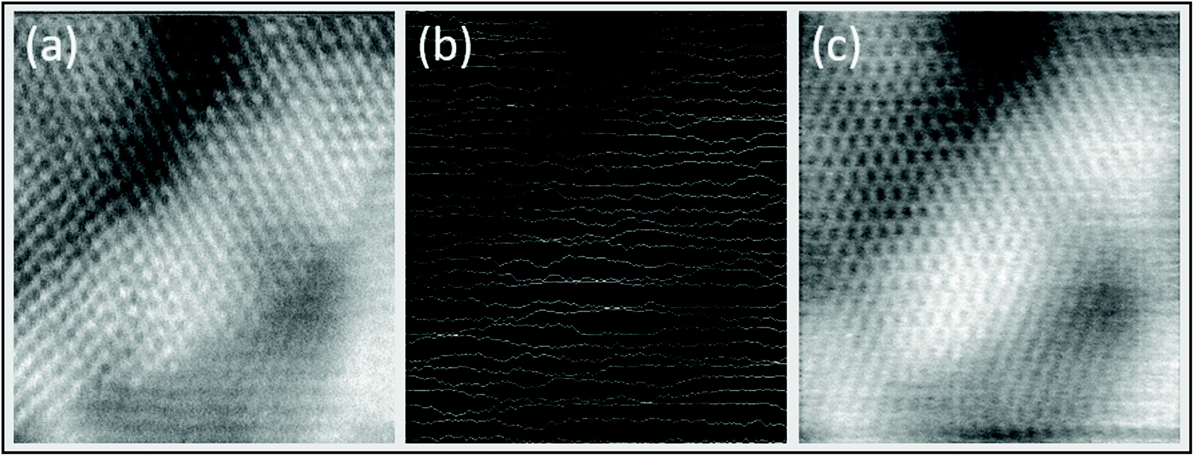 | ||
| Fig. 5 (a) An atomic resolution image of Ceria obtained using a 100% sampled 512 × 512 raster scan (b) the same atomic resolution image of Ceria obtained with a 6.25% line-hop sub-sampling (c) the reconstruction of the sub-sampled image shown in part (b) using inpainting algorithms. Both of the experimental images (a and b) were captured using a JEOL 2100F aberration corrected scanning transmission electron microscope with a beam voltage of 200 keV and a dwell time of 30 μs. The majority of the fine atomic scale information is reproduced in the reconstruction, as is the changes in morphology that are present in the form of contrast variations. | ||
The analysis described in this manuscript simplifies analysis of the mechanisms responsible for the creation and propagation of electron beam damage so that the effect of the positioning with the beam can be investigated. Obviously, the separation of the beam during STEM analysis can be further optimized by incorporating more precise models for the damage mechanisms that occur in real materials. However, what is also clear from this analysis is that for cases where the precise damage mechanism is not known, we can empirically determine the optimal scanning conditions by testing the level of sub-sampling, dose/rate and speed of image acquisition independently. Furthermore, by introducing controlled changes to the materials being investigated we can also determine how small levels of impurities and structure changes/defects can quantitatively change damage propagation. This will be particularly important for in situ observations where sub-sampling has already demonstrated control over the kinetics of particular damage mediated nucleation and growth pathways.20
Data availability
The data that supports the findings of this study are available within the article and its ESI.†Conflicts of interest
There are no conflicts of interest to declare.Acknowledgements
This work was supported in part by a Laboratory Directed Research and Development (LDRD) program at the Pacific Northwest National Laboratory (PNNL). PNNL is operated by Battelle Memorial Institute for the U.S. Department of Energy (DOE) under Contract No. DE-AC05-76RL01830. A portion of this research used the Environmental Molecular Sciences Laboratory (EMSL), a national scientific user facility sponsored by the DOE's Office of Biological and Environmental Research and located at PNNL. Aspects of this work were also supported in part by the UK Faraday Institution (EP/S003053/1) through awards FIRG013 “characterization”, FIRG005 “ReLiB” and FIRG001 “Degradation”.References
- P. Batson, N. Dellby and O. L. Krivanek, Nature, 2002, 418, 617 CrossRef CAS.
- O. L. Krivanek, P. D. Nellist, N. Dellby, M. F. Murfitt and Z. Szilagyi, Ultramicroscopy, 2003, 96(3–4), 229 CrossRef CAS.
- M. Isaacson, D. Johnson and A. V. Crewe, Radiat. Res., 1973, 55, 205 CrossRef CAS; P. Abellan, T. J. Woehl, L. R. Parent, N. D. Browning, J. E. Evans and I. Arslan, Chem. Commun., 2014, 50(38), 4873 RSC.
- J. P. Buban, Q. Ramasse, B. Gipson, N. D. Browning and H. Stahlberg, J. Electron Microsc., 2010, 59(2), 103 CrossRef CAS.
- H. Gu, G. Li, C. Liu, F. Yuan, F. Han, L. Zhang and S. Wu, Sci. Rep., 2017, 7(1), 184 CrossRef.
- R. F. Egerton, Ultramicroscopy, 2013, 127, 100 CrossRef CAS.
- R. F. Egerton, P. Li and M. Malac, Micron, 2004, 35(6), 399 CrossRef CAS.
- A. C. Johnston-Peck, W. D. Yang, J. P. Winterstein, R. Sharma and A. A. Herzing, Micron, 2018, 115, 54 CrossRef CAS.
- D. B. Williams and C. B. Carter, Transmission Electron Microscopy, Springer, US, 2nd edn, 2009 Search PubMed.
- I. P. Jones, Chemical Microanalysis: Using Electron Beams, The Institute of Materials, London, 1992, p. 241 Search PubMed.
- L. Kovarik, A. Stevens, A. Liyu and N. D. Browning, Appl. Phys. Lett., 2016, 109(16), 164102 CrossRef.
- A. Stevens, H. Yang, L. Carin, I. Arslan and N. D. Browning, Microscopy, 2014, 63(1), 41 CrossRef.
- A. Stevens, L. Luzi, H. Yang, L. Kovarik, B. L. Mehdi, A. Liyu, M. E. Gehm and N. D. Browning, Appl. Phys. Lett., 2018, 112(4), 043104 CrossRef.
- A. Velazco, M. Nord, A. Béché and J. Verbeeck, Ultramicroscopy, 2020, 215, 113021 Search PubMed.
- D. C. Joy, A. D. Romig Jr. and J. I. Goldstein, Principles of Analytical Electron Microscopy, 1986 Search PubMed.
- M. Nastasi, J. W. Mayer and J. K. Hirvonen, Ion-solid Interactions: Fundamentals and Applications, 1996 Search PubMed.
- B. M. Iskakov, K. B. Baigisova and G. G. Bondarenko, Russ. Metall., 2015, 2015(5), 400 CrossRef.
- P. Wynblatt, J. Phys. Chem. Solids, 1968, 29, 215 CrossRef CAS.
- E. L. Cussler, Diffusion: Mass transfer in fluid systems, 1984 Search PubMed.
- B. L. Mehdi, A. Stevens, L. Kovarik, N. Jiang, H. Mehta, A. Liyu, S. Reehl, B. Standfill, L. Luzi, W. Hao, L. Bramer and N. D. Browning, Appl. Phys. Lett., 2019, 063102 CrossRef.
Footnote |
| † Electronic supplementary information (ESI) available: Line hop scanning fundamentals, the image comparison metrics used above, and the MATLAB code used in the simulations. See DOI: 10.1039/d0nr04589f |
| This journal is © The Royal Society of Chemistry 2020 |