
 Open Access Article
 This Open Access Article is licensed under a
 Creative Commons Attribution 3.0 Unported Licence
Atomic level termination for passivation and functionalisation of silicon surfaces†
Nicholas E.
Grant‡
 *a,
Alex I.
Pointon‡
a,
Richard
Jefferies
a,
Daniel
Hiller
b,
Yisong
Han
c,
Richard
Beanland
c,
Marc
Walker
c and
John D.
Murphy
*a
*a,
Alex I.
Pointon‡
a,
Richard
Jefferies
a,
Daniel
Hiller
b,
Yisong
Han
c,
Richard
Beanland
c,
Marc
Walker
c and
John D.
Murphy
*a
aSchool of Engineering, University of Warwick, Coventry, CV4 7AL, UK. E-mail: nicholas.e.grant@warwick.ac.uk; john.d.murphy@warwick.ac.uk
bResearch School of Engineering, Australian National University, Canberra, ACT 2601, Australia
cDepartment of Physics, University of Warwick, Coventry, CV4 7AL, UK
First published on 13th August 2020
Abstract
Chemical treatments play an essential role in the formation of high quality interfaces between materials, including in semiconductor devices, and in the functionalisation of surfaces. We have investigated the effects of hydrogen and fluorine termination of (100)-orientation silicon surfaces over a range of length scales. At the centimetre scale, lifetime measurements show clean silicon surfaces can be temporarily passivated by a short treatment in both HF(2%)![[thin space (1/6-em)]](https://www.rsc.org/images/entities/char_2009.gif) :HCl(2%) and HF(50%) solutions. The lifetime, and hence surface passivation, becomes better with immersion time in the former, and worse with immersion time in the latter. At the nanometre scale, X-ray photoelectron spectroscopy and atomic force microscopy show treatment with strong HF solutions results in a roughened fluorine-terminated surface. Subsequent superacid-derived surface passivation on different chemically treated surfaces shows considerably better passivation on surfaces treated with HF(2%):HCl(2%) compared to HF. Lifetime data are modelled to understand the termination in terms of chemical and field effect passivation at the centimetre scale. Surfaces passivated with Al2O3 grown by atomic layer deposition behave similarly when either HF(2%):HCl(2%) or HF(50%) are used as a pre-treatment, possibly because of the thin silicon dioxide interlayer which subsequently forms. Our study highlights that chemical pre-treatments can be extremely important in the creation of high quality functionalised surfaces.
:HCl(2%) and HF(50%) solutions. The lifetime, and hence surface passivation, becomes better with immersion time in the former, and worse with immersion time in the latter. At the nanometre scale, X-ray photoelectron spectroscopy and atomic force microscopy show treatment with strong HF solutions results in a roughened fluorine-terminated surface. Subsequent superacid-derived surface passivation on different chemically treated surfaces shows considerably better passivation on surfaces treated with HF(2%):HCl(2%) compared to HF. Lifetime data are modelled to understand the termination in terms of chemical and field effect passivation at the centimetre scale. Surfaces passivated with Al2O3 grown by atomic layer deposition behave similarly when either HF(2%):HCl(2%) or HF(50%) are used as a pre-treatment, possibly because of the thin silicon dioxide interlayer which subsequently forms. Our study highlights that chemical pre-treatments can be extremely important in the creation of high quality functionalised surfaces.
1. Introduction
Silicon materials lie at the heart of many electronic devices, including the vast majority of photovoltaic solar cells. Atomic level control of the interface between silicon and the materials deposited upon it is vital for reliable and efficient device operation. Chemical cleaning and etching processes are well established for surface preparation for electronic device fabrication.1 Hydrogen termination of the surface is usually the first step of subsequent functionalisation, and an initially well or poorly treated surface can become apparent in subsequent device performance.2 The importance of silicon surface termination extends well beyond the electronic device community with, for example, hydrogen termination being a necessary first step in attaching DNA to a silicon surface for analysis and modification,3 and for various optical devices, biomedical devices, and sensors.4An important factor in silicon's dominance as an electronic material is that its surface properties can be controlled precisely with simple thermal and chemical processing. A thin native oxide forms over time in air (or thermal oxides can be grown at elevated temperature), and oxides can be easily removed in hydrofluoric acid (HF). The science of silicon surfaces in the presence of HF is covered in several reviews,5,6 and there are a number of subtleties. It is well established that a short treatment in a dilute HF solution results in a metastable hydrogen-terminated surface,7 however Si–F bonds are considerably stronger than Si–H bonds,7 and fluorine-terminated surfaces are known to result from treatments in concentrated HF.8,9 Control of the surface termination chemistry can be gained by adjusting the acidity of the solution,10 and the addition of hydrochloric acid (HCl) achieves hydrogen termination while not etching the bare silicon beneath.11
While there have been a large number of studies regarding the science of HF treated surfaces5,6 – a reflection of its importance in semiconductor manufacturing – there are no studies (to our knowledge) which address surface passivation at the macroscopic (e.g. centimetre) scale once the sample is removed from the solution. Most analytical techniques employed to examine the silicon surface post treatment are performed on the nanometre to micron scale. Although this helps determine what species are terminating the silicon surface post HF dip (e.g. H, F, OH) it does not quantify how many silicon bonds are terminated by these species, which in most device applications is crucial for increased functionalisation and spatial uniformity across the silicon surface. Therefore, to complement the scientific insight brought about by identifying the terminating species post HF dip, it is important to quantify the level of bond termination over a very large area. To the best of our knowledge, this can only currently be done by measuring the rate of surface recombination at the terminated silicon surface by a carrier lifetime measurement (such as by photoconductance decay12 or by photoluminescence imaging13) that can perform measurements on the timescale of milliseconds or longer. Providing these measurement techniques give a sufficient level of sensitivity, such techniques would be valuable in optimising the HF treatment, and thus maximising functionalisation of the silicon surface.
An example where this would be of significant value is when the silicon surfaces are treated with bis(trifluoromethanesulfonyl)-based solutions, including the superacid bis(trifluoromethane)sulfonimide (TFSI).14–18 The level of passivation achieved with these treatments is considerably greater than from just an HF dip and this is partly because of the existence of a charged layer on the surface which provides field effect passivation by repelling charge carriers away from the surface.16 However the extent to which these bis(trifluoromethanesulfonyl)-based passivation processes are affected by the prior surface treatments is not well established, because the impact (and effectiveness) of the HF termination has not been clearly demonstrated on a macroscopic scale.
This paper investigates the relevance (and impact) of using a macroscopic analytical method to maximise silicon surface termination by optimising the HF treatment to enhance surface functionalisation. We report the results of experiments to investigate the effects of surface termination of silicon at an atomic scale. We use injection-dependent carrier lifetime measurements on high lifetime float-zone silicon as a sensitive probe of the surface passivation arising from different chemical treatments. We then functionalise the terminated surface using a superacid-derived passivation process, finding that the different initial chemical treatments strongly affect the level of passivation achieved subsequently. By modelling the variation of carrier lifetime with excess carrier density, we are able to separate contributions arising from chemical and field effect passivation. To understand the physical origins of the behaviour observed we study the treated surfaces by X-ray photoelectron spectroscopy (XPS) and atomic force microscopy (AFM). Finally, we demonstrate that the effects of the chemical treatments are not always apparent, and are lost entirely when Al2O3 dielectric passivation is deposited on the treated surface by atomic layer deposition (ALD). To help understand this we use annular dark field scanning transmission electron microscopy (ADF-STEM) with energy dispersive X-ray (EDX) analysis to characterise the interfaces at the atomic scale.
2. Results
(a) Effective lifetime experiments and modelling
The extent to which a semiconductor surface is passivated can be quantified by measuring the effective carrier lifetime, τeffective, which to a good approximation for our experiments varies according to: | (1) |
Effective carrier lifetime results for chemically treated TMAH etched 5 Ω cm n-type float-zone silicon (FZ-Si) are shown in Fig. 1. Fig. 1(a) shows that treatment with either HF(50%) or HF(2%):HCl(2%) passivates the surface when the silicon samples are pulled dry from the solutions (i.e. no deionised water rinse is performed), which mitigates the formation of a hydroxylised surface when H and F related species are washed away during a rinse.19 Samples were therefore not rinsed in order to retain a well passivated surface. Control samples which had not received an HF-based treatment after cleaning showed lifetimes well below the worst lifetimes in Fig. 1 (see ESI, Fig. S1(a)†).
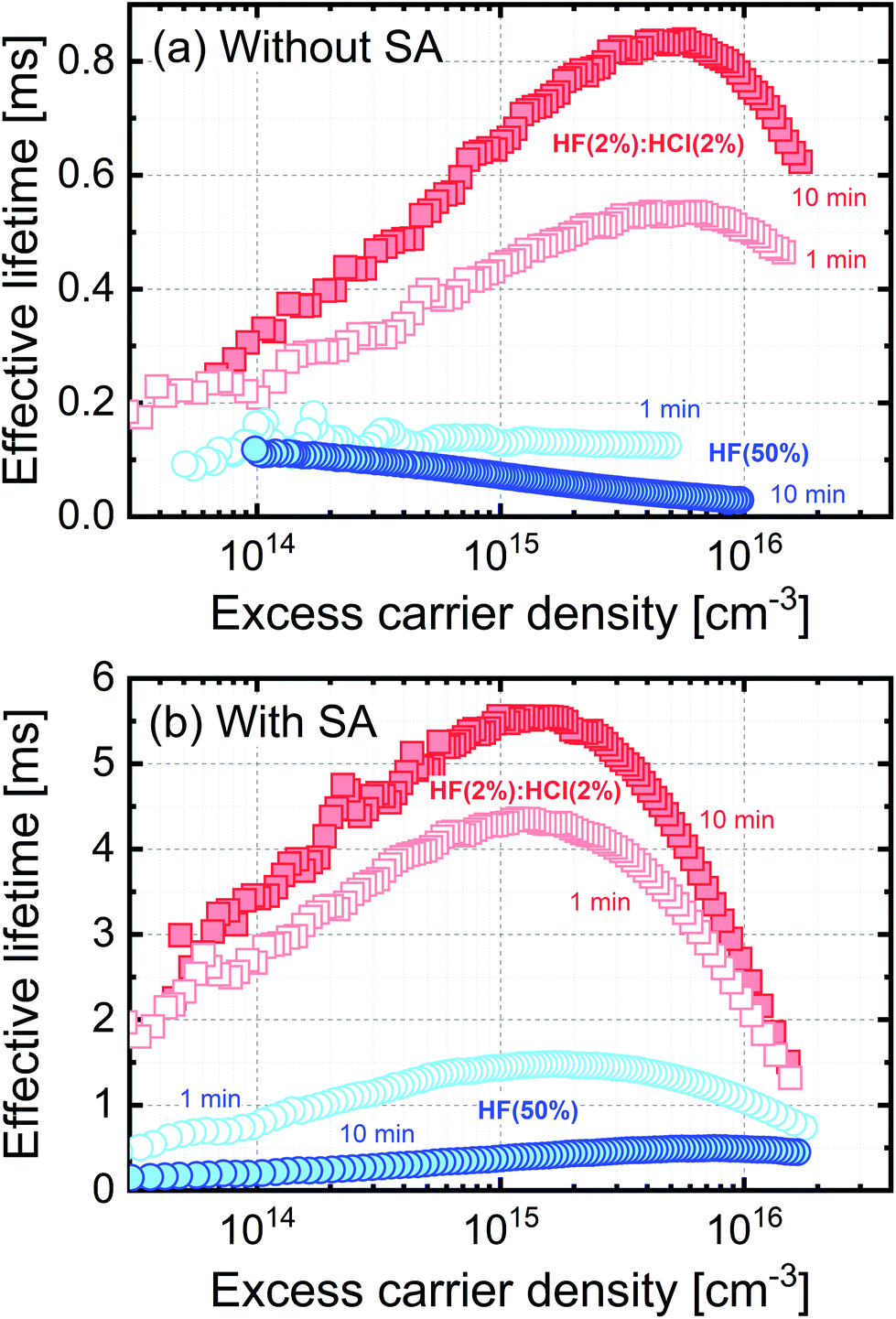 | ||
| Fig. 1 Effective lifetime versus excess carrier density for 700 μm thick 5 Ω cm n-type TMAH etched silicon wafers. In (a) the samples are subjected to HF(2%):HCl(2%) or HF (50%) treatments for the times stated, and in (b) a TFSI-pentane superacid-derived surface passivation scheme (SA) is applied in addition. Lifetimes for control samples which did not receive a HF-based treatment after cleaning are very low, and are shown in the ESI (Fig. S1†). Data for planar etched silicon are also shown in the ESI (Fig. S2†). | ||
Performing a longer treatment in HF(2%):HCl(2%) results in better surface passivation than a shorter treatment. Perhaps surprisingly, the passivating effect of HF(50%) gets worse with the length of treatment time, and we explain this later. The effects observed are independent of the surface's starting condition, as similar trends are observed for smooth planar etched silicon samples (see ESI, Fig. S2†) and for TMAH etched surfaces which are relatively rough at the nanometre scale (see AFM map in our previous publication15). Our results for planar etched surfaces in Fig. S2† also show that treatment with just HF(2%) without HCl results in a lower lifetime than with HF(2%):HCl(2%) showing that the presence of HCl in the solution results in better passivation.
Data in Fig. 1(b) show the effect of an additional superacid-derived passivation treatment (using TFSI-pentane for 60 s in all cases) applied after the same pre-treatments as in Fig. 1(a). The additional superacid-derived passivation increases the effective lifetimes showing that the values presented in Fig. 1(a) are not limited by the bulk lifetime. Importantly, the contribution of the different pre-treatments is still apparent after the superacid-derived treatment, with the same trends observed as in Fig. 1(a). This highlights the importance of chemical process history in producing a functionalised or passivated sample surface in at least some cases. The lifetime in control samples which had not received an HF-based treatment after cleaning remains low (ESI, Fig. S1(b)†).
Fig. 2 summarises the effect on effective lifetime of the different treatments on TMAH etched silicon without and with superacid-derived surface passivation at a fixed excess carrier density of 1 × 1015 cm−3. A similar plot for treated planar etched silicon is included in the ESI (Fig. S3†). For each treatment it is clear that the superacid-derived passivation enhances lifetime substantially. The ratio of values at the chosen excess carrier density is between 5.2 and 11.1 times for the conditions studied. It is noted that the interplay between the different passivation schemes and mechanisms is complex, yet more insight can be gained by analysing the injection dependence of the effective lifetime.
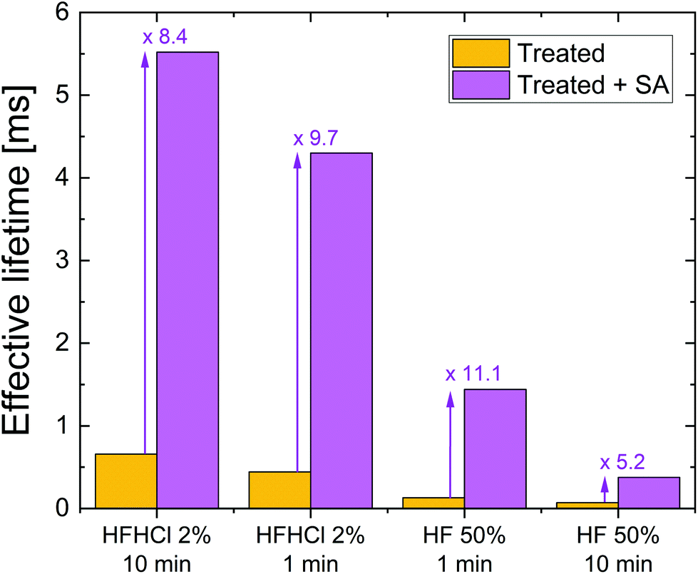 | ||
| Fig. 2 Effective lifetime at an excess carrier density of 1015 cm−3 for 700 μm thick 5 Ω cm n-type TMAH etched silicon wafers. The left bar of each pair shows the effect of the stated treatment only, whereas the right bar shows the effect of the stated treatment plus an additional TFSI-pentane superacid-derived surface passivation scheme (SA). The factor by which the superacid-derived passivation enhances lifetime is stated. Data for planar etched silicon are shown in the ESI (Fig. S3†). | ||
Surface passivation of semiconductors is governed by the extent to which dangling bonds are terminated (“chemical” passivation) and the level of charge in the passivating layer which modifies the distribution of carriers near the semiconductor's surface (“field effect” passivation). For fixed capture parameters, chemical passivation can be quantified by the reduction in interface state density (Dit), with the level of field effect passivation determined by the effective areal charge density (Qeff). In high quality silicon with a low concentration of bulk recombination centres, such as that used here, these parameters strongly influence the dependence of carrier lifetime on excess carrier density. Fig. 3 shows fitting of experimental lifetime curves using software available from PV Lighthouse20 based on a method described by Girisch et al.21 which was extended by Aberle et al.22 For the fitting we assume that surface recombination is governed by a single defect at mid-gap and use the intrinsic recombination parameterisation of Richter et al.23 The fit parameter for chemical passivation is a carrier type-specific surface recombination parameter, and for electrons is Sn0 = vtn × σn × Dit and for holes is Sp0 = vtp × σp × Dit, where vtn is the thermal velocity of electrons and vtp is the thermal velocity of holes, and σn and σp are the capture cross-sections for electrons and holes, respectively. It is not possible to separate the cross-section and interface state density terms from the analysis of lifetime data alone.
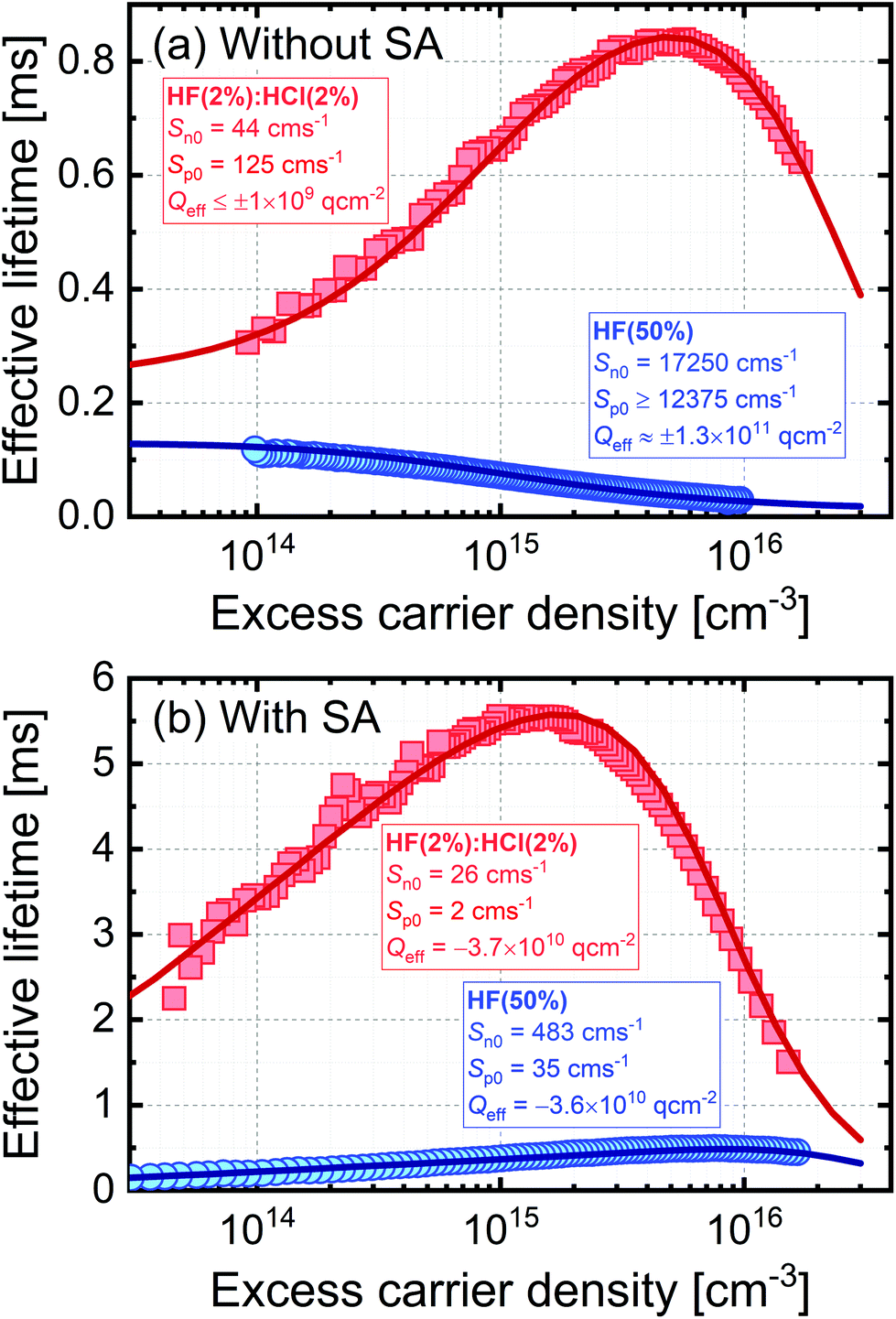 | ||
| Fig. 3 Modelling of effective lifetime as a function of excess carrier density for 700 μm thick 5 Ω cm n-type silicon using the extrema of the experimental data for TMAH etched silicon in Fig. 1 (all with 10 min treatment times). Plot (a) is for samples subjected to just HF(2%):HCl(2%) or HF(50%) treatments, and samples for plot (b) also received a TFSI-pentane superacid-derived passivation scheme (SA). As described in the text, a model was used to produce the solid lines, which provided a good fit to the experimental data with the parameters stated. | ||
Fig. 3 presents the fits to the extreme datasets for the TMAH etched samples in Fig. 1, i.e. those giving the highest and lowest lifetimes (a) in the absence and (b) in the presence of additional superacid-derived passivation. Fits to selected lifetime curves for planar silicon etched samples are provided in the ESI (Fig. S4†). Good fits to the experimental data can be made in all cases, with the parameters used given on the graphs. In the absence of additional superacid-derived passivation in Fig. 3(a), the 10 min HF(2%):HCl(2%) treatment results in low values of Sn0 and Sp0, which is likely because the treatment gives rise to good chemical passivation by reducing Dit. Conversely, the 10 min HF(50%) treatment has very high values of Sn0 and Sp0 which shows this treatment results in a poor level of chemical passivation. The level of field effect passivation arising from the HF(2%):HCl(2%) treatment is low (Qeff of order 109 q cm−2) and the experimental lifetime curves can be accurately modelled using either charge polarity, indicating the surface charge is too low to have any significant impact on the level of passivation in this case. The 10 min HF(50%) treatment has a much stronger field effect component. In this case it is not possible to extract the charge polarity unambiguously, but a magnitude of Qeff ∼1 × 10¹¹ q cm−2 is consistent with the lifetime data, as shown by fits for different charge densities provided in the ESI (Fig. S5†).
Fig. 3(b) shows the effect of an additional superacid-derived surface treatment. For the sample first subjected to a 10 min HF(2%):HCl(2%) treatment, the additional TFSI-pentane treatment improves both the chemical passivation (further reducing Sn0 and Sp0) and also the field effect passivation. For this case, a negative Qeff is required with a magnitude of 3.7 × 10¹⁰ q cm−2. The inference of negative charge agrees with previous Kelvin probe studies of TFSI-based passivation of silicon,16 and the magnitude of the charge is similar to that found for silicon passivated with a range of bis(trifluoromethanesulfonyl)-based solutions which find negative values in the range 6–9 × 10¹⁰ q cm−2.16,17 The results for the 10 min HF(50%) treatment in Fig. 3(b) show an improvement in chemical passivation (reduced Sn0 and Sp0) as a result of the TFSI-pentane passivation, and a similar level of field effect passivation to the HF(2%):HCl(2%) case. In summary, the results in Fig. 3(b) show that the superacid-derived treatment provides a similar level of field effect passivation regardless of the pre-treatment, but that the level of chemical passivation remains strongly influenced by the surface pre-treatment performed prior to the superacid-derived passivation step. Therefore, by measuring the effective lifetime directly after the HF dip, we can assess the level and effectiveness of the surface termination, and how this will impact the functionalisation of the silicon surface when subsequently SA treated. The high lifetimes reported in Fig. 3(b) also confirm how effective superacid-derived treatments can be at passivating silicon surfaces, as thin films which form after removal from superacidic solutions provide equivalent passivation to when silicon is fully immersed in liquid HF.24
Fitting of lifetime curves for planar etched surfaces tells a similar story (Fig. S4†). The values for Sn0, Sp0 and Qeff are slightly different to those for the TMAH etched case in the absence of superacid-derived passivation, but are very similar after the superacid-derived passivation. In the planar etched case, a small density of negative charge is required to fit the data before the additional passivation, and such a difference is justifiable given the considerable differences between the types of etching.
(b) Surface characterisation
Cleaned silicon samples subjected to 10 min HF(50%) and HF(2%):HCl(2%) treatments were characterised by XPS after being pulled dry from their respective solution, with key results shown in Fig. 4. The data shown are for a shallow take-off angle of 15° with respect to the surface parallel as this gives a relatively good sensitivity for surface studies. Data for a 90° take-off angle are included in the ESI (Fig. S6†), as is a table of elemental compositions (Table S1†).
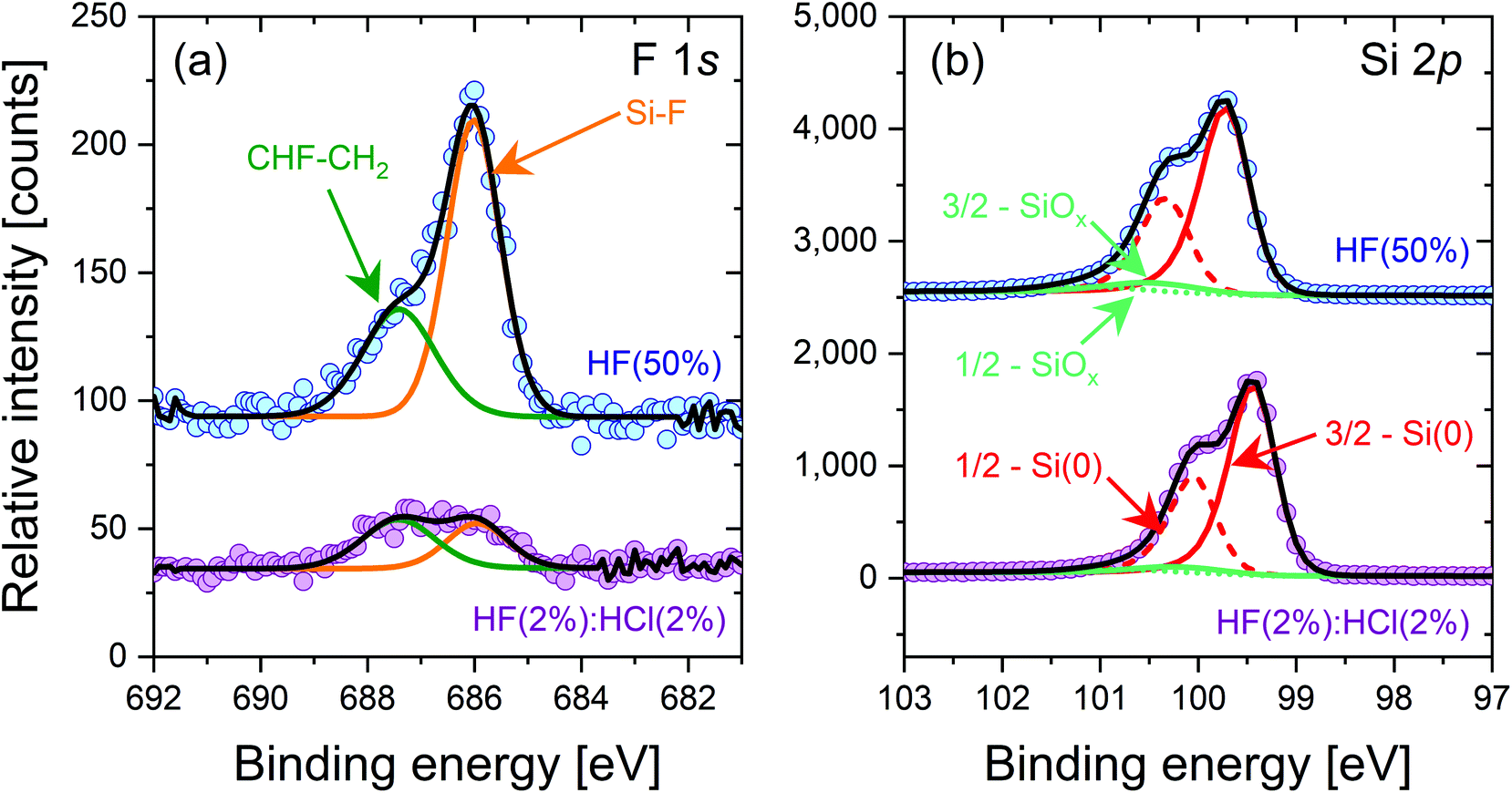 | ||
| Fig. 4 XPS spectra at take-off angle of 15° with respect to the surface parallel for 5 Ω cm n-type FZ-Si treated for 10 min with HF(50%) at the top, and HF(2%):HCl(2%) at the bottom. Spectra have been offset in the vertical direction for clarity. The F 1s spectra (left) show substantially enhanced fluorine termination in the HF(50%) case. The Si 2p spectra (right) are similar for both treatments, showing any SiOx layer is thin. Additional superacid-derived passivation was not applied. | ||
The F 1s spectra in Fig. 4(a) shows a substantially larger Si–F peak for a 10 min HF(50%) treatment compared to a 10 min HF(2%):HCl(2%) treatment. The CHF–CH2 peak is also larger. This shows that more fluorine termination occurs in the case of the HF(50%) treatment. Fig. 4(b) shows the Si 2p spectra, which are similar for both samples. There are small SiOx-related peaks in both samples, which may arise from thin oxide layers formed during the transfer of the samples from the cleanroom to the XPS system. Cl 2s spectra were also recorded but showed no Cl-related peaks for either sample in the 260 to 280 eV binding energy range. Unfortunately our XPS experiments do not provide reliable information on hydrogen termination. Direct detection is not possible because of hydrogen's small photoionisation cross-section, and any hydrogen-related change in the Si 2p peak position sometimes used to assess hydrogen termination25 is likely to be affected by the co-existence of fluorine resulting from our HF-based wet chemical treatments.
To investigate the surface topology, AFM maps were acquired for samples subjected to 10 min HF(50%) and HF(2%):HCl(2%) treatments and the results are shown in Fig. 5. The sample treated with HF(50%) was found to be decorated with nano-particulates at the surface, whereas no such particles are found in the HF(2%):HCl(2%) case. The particles have a typical dimension of 2 nm to 6 nm from the surface. It therefore appears that an extended etch in concentrated HF damages the surface in some way and this, as well as fluorine termination, may account for the lower levels of surface passivation achieved.
 | ||
| Fig. 5 Representative 25 μm × 25 μm AFM maps of 5 Ω cm n-type FZ-Si after (a) an HF(50%) treatment for 10 min and (b) an HF(2%):HCl(2%) treatment for 10 min. Neither sample had been subsequently treated with superacid-derived passivation. The horizontal line scans in (c) show scans typical of both sample types. | ||
(c) Surface termination for dielectric-based passivating films
For stable passivation in electronic devices, such as silicon solar cells, thin films of dielectric materials are typically used (see ref. 26 for a review). As we have established that the effect of the chemical pre-treatment persists after superacid-derived passivation (see Fig. 1(b), 2 and 3(b)), it is important to assess whether this might be the case for dielectric deposition. Using atomic layer deposition (ALD) we deposited 20 nm thick aluminium oxide films on the surface of n-type Cz-Si samples from the same wafer pre-treated with HF(50%) or HF(2%):HCl(2%) for 10 min (where the samples were pulled dry from their respective solution). The process comprises a deposition step at 200 °C followed by a 460 °C activation anneal. The injection-dependent effective lifetime results are shown in Fig. 6.
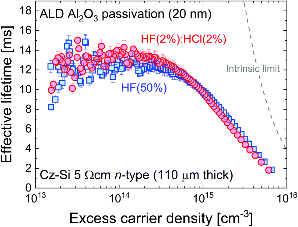 | ||
| Fig. 6 Effective lifetime versus excess carrier density for 110 μm thick 5 Ω cm n-type Cz-Si samples from the same wafer treated with HF(2%):HCl(2%) or HF(50%) for 10 min immediately before the ALD process (200 °C deposition with 460 °C activation). The level of surface passivation is the same within the 5% error shown, unlike for the superacid-derived passivation in Fig. 1(b). The intrinsic lifetime limit from Richter et al.23 is also shown. | ||
It is clear from Fig. 6 that the pre-treatment makes no significant difference to the level of ALD passivation achieved within the typical errors of lifetime measurement (error bars of 5% are shown, guided by ref. 27). The difference from the chemical pre-treatment appears to have been eliminated during the Al2O3 growth and activation process. While this is an important result, it is noted that the surface preparation prior to Al2O3 deposition can still make a difference if the surface is not treated prior to deposition to remove SiO2 layers which form during sample cleaning. In the ESI (Fig. S7†) we show that much worse surface passivation results when the samples are not treated with a HF-based solution after SC1 or SC2 cleaning. It is worth noting that the level of passivation achieved in Fig. 6 is state-of-the-art. At an excess carrier density of 1 × 1015 cm−3, using Eqn (1) with τbulk as the intrinsic limit from Richter et al.23 gives S as 0.45 cm s−1. Thus, although the HF(50%) chemical treatment appears not to give the optimal conditions initially, its effect is not relevant once a high quality dielectric has been deposited. To elucidate this finding, we have examined the interface between the silicon and the ALD Al2O3 layer by STEM with EDX analysis before and after the activation anneal, with the results presented in Fig. 7.
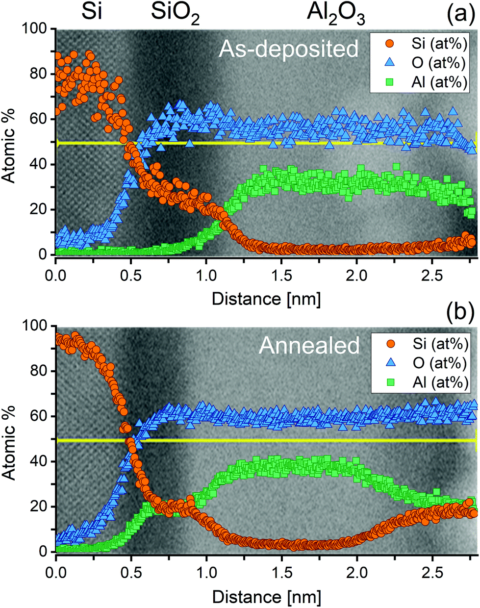 | ||
| Fig. 7 ADF-STEM and the corresponding EDX line scan measurements of a silicon sample coated by ALD Al2O3 in (a) the as-deposited case, and (b) after annealing in air at 460 °C for 30 min. The EDX data were acquired along the yellow line plotted. For these samples, the surface was treated in an HF(2%) for ∼10 s and samples were pulled dry prior to deposition. The apparent shift in the SiO2 position between (a) and (b) is due to a slightly different starting position. | ||
Fig. 7 shows ADF-STEM images of an Al2O3 film coated on a silicon substrate (a) in the as-deposited case and (b) after post annealing in air at 460 °C for 30 min. To determine the composition of each region in the STEM images, we have also performed EDX measurements, which have been overlaid on to the corresponding STEM images in Fig. 7. The apparent gradient of composition at the interfaces is due to spreading of the electron beam as it propagates through the specimen (∼100 nm in thickness).
From the combined STEM and EDX measurements, it is evident that a thin (0.45–0.5 nm) SiO2 layer is present post deposition, and that this oxide remains after a 30 min 460 °C anneal in air, albeit slightly thinner in the latter case (∼0.4 nm). Furthermore, a significant amount of Al has diffused into the native oxide, which remains amorphous but with a composition Si0.5Al0.5O2. It is worth noting that most films deposited by ALD do exhibit a thin silicon dioxide layer sandwiched between the silicon substrate and thin film,28–31 even when the dielectric being deposited does not use an oxygen containing precursor or co-reactant. An example of this can be seen in the ESI (Fig. S8†) which shows the existence of a ∼1.5 nm SiO2 film underneath a thin silicon nitride (Si3N4) layer by XPS. Based on our results for ALD Al2O3 surface passivation, we conclude that, despite the difference in surface termination by a HF(2%):HCl(2%) and HF(50%) treatment, the growth of a thin silicon dioxide layer during the ALD deposition prohibits any variation of the electrical quality of the ALD film caused by the type of final dip treatment. However, other low temperature deposition techniques (e.g. plasma-enhanced chemical vapour deposition) may result in different behaviour.
3. Discussion
(a) Surface treatments and termination
Our method of measuring lifetimes a few seconds after removal from the HF or HF:HCl solutions without rinsing enables the surface termination effects of the treatments to be assessed out of solution. Passivation arises in all cases (Fig. 1(a)), although the level of passivation is strongly dependent on the solution's composition and duration of treatment. Previous studies measured lifetimes with samples immersed in acidic solutions32–34 and the differences between the chemical treatments are less apparent (reviewed in ref. 24). Our data clearly show that out-of-solution HF(2%):HCl(2%) treatments offer better passivation than HF(50%), and that this passivation improves with immersion time in the former but gets worse with time in the latter. The modelling results (Fig. 3(a)) show that the superiority of HF(2%):HCl(2%) over HF(50%) is because of lower Sn0 and Sp0 values, which is most likely because of better chemical passivation of the surface (lower Dit values assuming fixed capture parameters).
The presence of HCl in the HF solution affects the surface termination in at least three ways. Firstly, it cleans impurities (mostly metals) away from the silicon surface which is why it is used in Standard Clean 2 (SC2) as part of RCA cleaning.1 Secondly, it reduces the pH of the solution as the ionic hydrogen concentration is higher,10 hence aiding Si–H surface termination. Thirdly, it reduces the concentration of fluoride ions in the solution,10 and hence reduces the formation of bonds with fluorine species. The addition of HCl has also been found to be beneficial when the lifetime is measured with the sample immersed in an HF-containing solution,34 probably for the same reasons as here. We suggest that HCl addition to HF-containing solutions could be beneficial for the creation of a high-quality hydrogen-terminated surface required for a range of applications (e.g. DNA attachment to a silicon surface3).
Treatments in concentrated HF solutions result in a different surface termination chemistry compared to HF:HCl solutions. Fig. 1(a) shows a 1 min treatment in HF(50%) results in better passivation than a 10 min treatment. Our explanation is that the initial metastable hydrogen termination is reduced as the level of fluorine termination increases with immersion time. The fluorine concentration will be much higher than in the HF(2%):HCl(2%) solution and the hydrogen concentration lower.10 There is clear evidence for Si–F bonding in HF(50%) samples treated for 10 min in the XPS data in Fig. 4(a), and similar findings have been published previously.8,9 The fact that Si–F bonds form over time is expected thermodynamically given the bond dissociation energies of Si–F are perhaps the strongest single bonds known,9 and are almost a factor of two higher than Si–H.7,35
As well as the surface termination, the surfaces themselves are different as a consequence of the treatments (Fig. 5). As expected from the findings of an earlier AFM study,11 HF-HCl treatments do not roughen the surface. Prolonged treatment in concentrated HF appears to result in a roughened surface, as has been found previously for silicon treated in strong HF solutions.10 Trucks et al. explain the difference in surface behaviour in terms of polarisation of the Si–Si bonds, which can be broken by dipolar HF, whereas a hydrogen-terminated surface is stable due to the lack of polarisation of adjacent Si–Si bonds.7
(b) Additional passivation after chemical treatments
We have systematically studied the application of two different surface passivation schemes after the different chemical surface treatments, and substantial differences were found between the cases. For superacid-derived passivation, the passivation trends (Fig. 1(b)) follow those of the underlying surface treatment (Fig. 1(a)). For ALD-grown Al2O3 passivation, the surface pre-treatment seems to be irrelevant after the passivation is applied. Fig. 6 shows that excellent levels of passivation (S < 0.5 cm s−1) can be achieved even with the poorest performing surface treatment.The lack of difference in ALD Al2O3 passivation when the surface is either fluorine or hydrogen terminated is an important finding of this study. As is usual for this passivation system,36 we perform the ALD deposition at low temperature (200 °C) and then perform a higher temperature (460 °C) ex situ anneal to “activate” the passivation. While it is possible that the surface termination affects the properties of the passivating film during the process (pre-hydrogenation affects the ALD growth,37 for example), the final outcome is that the passivation is independent of the initial surface treatment. Furthermore, ALD is an exceptionally good approach for coating silicon surface features at the nm scale,38 so any surface damage caused by the concentrated HF treatment seems to be equally well passivated as the undamaged surface. As ALD Al2O3 passivation is widely used in silicon solar cell fabrication, the fact that the details of the HF treatment prior to passivation is relatively unimportant is convenient for cell manufacturers.
There could be a number of reasons why there is a difference in behaviour between superacid-derived passivation and ALD Al2O3 passivation. The temperatures of the processes are very different, but this may not be the only factor. We note that Takahagi et al. studied room temperature oxidation of silicon pre-treated with HF(1%) and HF(50%) and found no difference in the growth rate,8 whereas in our room temperature superacid-derived process we find a large difference in passivation behaviour with different surface treatments. In the ALD process the reactions with precursors could render the initial surface treatment irrelevant due to the formation of a thin silicon dioxide layer, as evident from our STEM and EDX results for Al2O3 and XPS results for Si3N4.
4. Conclusions
We have performed a sensitive study into how surface treatments affect the passivation and subsequent functionalisation of (100)-orientation silicon wafers at the macroscopic scale. Treatment with HF(50%) leads to fluorine termination and a damaged surface, whereas treatment with HF(2%):HCl(2%) leads to a damage-free surface which is likely to be hydrogen terminated. Differences in termination are relevant for some subsequent surface functionalisation processes, but not others. Importantly, whether the surface is hydrogen or fluorine terminated seems to be irrelevant from the perspective of achieving state-of-the-art surface passivation with ALD Al2O3, with surface recombination velocities of 0.45 cm s−1 achieved in both cases. However, we demonstrate that the surface termination is important for other surface functionalisation, such as when superacid-derived passivation is applied to the surface, with a weak aqueous solution of HF and HCl giving the best results.
5. Experimental section
(a) Chemical pre-treatment lifetime experiments
Lifetime pre-treatment experiments were conducted on 700 μm thick 5 Ω cm n-type (100)-orientation 100 mm diameter float-zone silicon (FZ-Si) wafers. Large quarter wafer samples were used to minimise recombination at the sample edges.39 Samples were subjected to a rigorous cleaning procedure developed previously15 in which all solutions are aqueous, all percentages are by volume (throughout this paper), and the water used was de-ionised (DI) with a measured resistivity of 18.2 MΩ cm and a total organic impurity level of <5 parts per billion. The standard cleaning procedure was: (i) a dip in 1% HF to remove any native oxide; (ii) a standard clean 2 (SC2) process consisting of H2O, H2O2 (30%), HCl (37%) (5:1:1) for 10 min at ∼80 °C; (iii) a dip in 1% HF to remove the chemical oxide formed by SC2; (iv) an etch in 25% tetramethylammonium hydroxide (TMAH) for 10 min at ∼80 °C or a planar silicon etch comprising HNO3 (69.5%) and HF (50%) (10:1) for 5 min after being allowed to come to temperature for 15 min without external heating; and (v) another dip in 1% HF followed by another SC2 clean for 10 min at ∼80 °C. Samples were then subjected to a treatment in HF (usually 50%) or HF(2%):HCl(2%) for either 1 or 10 min. Importantly, to mitigate washing away H and F related species, the samples were pulled dry from the HF-containing solutions (i.e. no deionised water rinse is performed following the HF dips). The chemical treatments were performed in a cleanroom environment with a relative humidity of 53–54% and a temperature of 21–22 °C.
(b) Superacid-derived passivation process
Precursor chemicals were handled and stored in a high specification glovebox (a sealed filtered MBRAUN UNIlab modular glovebox workstation) with gas purification system and solvent filter with a controlled low humidity atmosphere (<0.1 ppm O2; <0.1 ppm H2O). 400 mg of bis(trifluoromethane)sulfonimide (TFSI) crystals from Sigma-Aldrich (>95% purity) were dissolved in 200 ml of anhydrous pentane from Sigma-Aldrich (>99% purity). The superacidic solution was then removed from the controlled environment in a sealed bottle and transferred to the cleanroom. Silicon samples were immersed in the solutions for 60 s at room temperature before being removed and allowed to dry in cleanroom air. This is a slight modification to the method used in our prior passivation studies15–18 in which the dipping and drying occurred in a glovebox and, although the passivation outside of a glovebox is marginally worse, it does enable lifetimes to be measured more rapidly as is required here.(c) ALD deposition processes
For ALD lifetime experiments, quarter wafer samples from 125 μm thick 5 Ω cm n-type (100)-orientation 156 mm diameter Czochralski silicon (Cz-Si) wafers were subjected to (i) a standard clean 1 (SC1) process comprising H2O, H2O2 (30%), NH4OH (30%) (5:1:1) at ∼80 °C for 10 min; (ii) a 1% HF dip; (iii) a 25% TMAH etch for 10 min at ∼80 °C; (iv) a 1% HF dip; (v) an SC2 clean for 10 min at ∼80 °C; and then (vi) a soak in HF (50%) or HF(2%):HCl(2%) for 10 min before being pulled dry (no DI water rinse). ALD was performed using a Veeco Fiji G2 system featuring an external load lock. Aluminium oxide was deposited at 200 °C using a plasma O2 source and a trimethylaluminium precursor for 200 cycles to give films ∼20 nm thick, with the process repeated for the second side of the sample. To activate the Al2O3 passivation, a post deposition anneal in air was performed in a quartz tube furnace at 460 ± 10 °C for 30 min.
For TEM and XPS experiments, ALD depositions were performed on 750 μm thick >2000 Ω cm (100)-orientation Cz-Si wafers. The same cleaning procedure as for the lifetime samples was used, with the final stage being a dip in HF(2%) for ∼10 s before the sample was pulled dry from the HF solution prior to deposition. For Al2O3, the same process was used as for lifetime samples above, except just 160 cycles were performed. Silicon nitride was deposited at 300 °C using an N2 plasma source and a bis(diethylamido)silane precursor for 300 cycles to give films ∼3.5 nm thick. Samples with silicon nitride films were not subjected to ex situ “activation” annealing.
(d) Characterisation
:HCl(2%). They were mounted on to copper stubs using electrically-conductive carbon tape and were loaded into a nitrogen-purged transfer container in cleanroom (not glovebox) conditions within two minutes of the final chemical process step. The XPS spectrometer base pressure was ∼1 × 10⁻¹⁰ mbar and samples were pumped to <1 × 10⁻⁶ mbar in the load lock before transfer within 1–2 h of the chemical treatment. XPS measurements were performed at room temperature using a monochromated Al Kα X-ray source with a take-off angle of 15° or 90° with respect to the surface parallel. The core level XPS spectra were recorded using a pass energy of 20 eV (resolution approximately 0.4 eV) from an analysis area of 300 μm × 700 μm. The spectrometer work function and binding energy scale were calibrated using the Fermi edge and 3d5/2 peak recorded from a polycrystalline Ag sample prior to the commencement of the experiments. Fitting procedures to extract peak positions and relative stoichiometries from the XPS data were carried out using the Casa XPS software suite, using Shirley backgrounds and mixed Gaussian–Lorentzian (Voigt) line shapes.
:HCl(2%) in order to minimise roughening of the surface.
Conflicts of interest
There are no conflicts of interest to declare.Acknowledgements
This work was supported by the EPSRC SuperSilicon PV project (EP/M024911/1) and the EPSRC Impact Acceleration Account (EP/R511808/1). A. I. Pointon is the recipient of an EPSRC studentship (EP/N509796/1). Data underpinning figures in this paper can be freely downloaded from https://wrap.warwick.ac.uk/139135. Requests for additional data should be made directly to the corresponding authors.References
- W. Kern, J. Electrochem. Soc., 1990, 137, 1887–1892 CrossRef CAS.
- H. F. Okorn-Schmidt, IBM J. Res. Dev., 1999, 43, 351–365 CAS.
- Z. Lin, T. Strother, W. Cai, X. Cao, L. M. Smith and R. J. Hamers, Langmuir, 2002, 18, 788–796 CrossRef CAS.
- J. Veerbeek and J. Huskens, Small Methods, 2017, 1, 1700072 CrossRef.
- K. Oura, G. Lifshits, A. A. Saranin, A. V. Zotov and M. Katayama, Surf. Sci. Rep., 1999, 35, 1–69 CrossRef CAS.
- J. M. Buriak, Chem. Rev., 2002, 102, 1271–1308 CrossRef CAS PubMed.
- G. W. Trucks, K. Raghavachari, G. S. Higashi and Y. J. Chabal, Phys. Rev. Lett., 1990, 65, 504–507 CrossRef CAS PubMed.
- T. Takahagi, A. Ishitani, H. Kuroda and Y. Nagasawa, J. Appl. Phys., 1991, 69, 803–807 CrossRef CAS.
- B. R. Weinberger, G. G. Peterson, T. C. Eschrich and H. A. Krasinski, J. Appl. Phys., 1986, 60, 3232–3234 CrossRef CAS.
- V. Bertagna, R. Erre, F. Rouelle and M. Chemla, J. Solid State Electrochem., 1999, 4, 42–51 CrossRef CAS.
- L. Li, H. Bender, T. Trenkler, P. W. Mertens, M. Meuris, W. Vandervorst and M. M. Heyns, J. Appl. Phys., 1995, 77, 1323–1325 CrossRef CAS.
- H. Nagel, C. Berge and A. G. Aberle, J. Appl. Phys., 1999, 86, 6218–6221 CrossRef CAS.
- T. Trupke, R. A. Bardos, M. C. Schubert and W. Warta, Appl. Phys. Lett., 2006, 89, 044107 CrossRef.
- J. Bullock, D. Kiriya, N. Grant, A. Azcatl, M. Hettick, T. Kho, P. Phang, H. C. Sio, D. Yan, D. Macdonald, M. A. Quevedo-Lopez, R. M. Wallace, A. Cuevas and A. Javey, ACS Appl. Mater. Interfaces, 2016, 8, 24205–24211 CrossRef CAS.
- N. E. Grant, T. Niewelt, N. R. Wilson, E. C. Wheeler-Jones, J. Bullock, M. Al-Amin, M. C. Schubert, A. C. van Veen, A. Javey and J. D. Murphy, IEEE J. Photovoltaics, 2017, 7, 1574–1583 Search PubMed.
- A. I. Pointon, N. E. Grant, R. S. Bonilla, E. C. Wheeler-Jones, M. Walker, P. R. Wilshaw, C. E. J. Dancer and J. D. Murphy, ACS Appl. Electron. Mater., 2019, 1, 1322–1329 CrossRef CAS.
- A. I. Pointon, N. E. Grant, S. L. Pain, J. T. White and J. D. Murphy, Appl. Phys. Lett., 2020, 116, 121601 CrossRef CAS.
- A. I. Pointon, N. E. Grant, E. C. Wheeler-Jones, P. P. Altermatt and J. D. Murphy, Sol. Energy Mater. Sol. Cells, 2018, 183, 164–172 CrossRef CAS.
- X. G. Zhang, Electrochemistry of Silicon and Its Oxide, Springer, 2001 Search PubMed.
- Calculator Map from PV Lighthouse http://www.pvlighthouse.com.au.
- R. B. M. Girisch, R. P. Mertens and R. F. De Keersmaecker, IEEE Trans. Electron Devices, 1988, 35, 203–222 CrossRef CAS.
- A. G. Aberle, S. Glunz and W. Warta, J. Appl. Phys., 1992, 71, 4422–4431 CrossRef CAS.
- A. Richter, S. W. Glunz, F. Werner, J. Schmidt and A. Cuevas, Phys. Rev. B: Condens. Matter Mater. Phys., 2012, 86, 165202 CrossRef.
- N. E. Grant and J. D. Murphy, Phys. Status Solidi RRL, 2017, 11, 1700243 CrossRef.
- C. J. Karlsson, F. Owman, E. Landemark, Y.-C. Chao, P. Mårtensson and R. I. G. Uhrberg, Phys. Rev. Lett., 1994, 72, 4145–4148 CrossRef CAS PubMed.
- R. S. Bonilla, B. Hoex, P. Hamer and P. R. Wilshaw, Phys. Status Solidi A, 2017, 214, 1700293 CrossRef.
- A. L. Blum, J. S. Swirhun, R. A. Sinton, F. Yan, S. Herasimenka, T. Roth, K. Lauer, J. Haunschild, B. Lim, K. Bothe, Z. Hameiri, B. Seipel, R. Xiong, M. Dhamrin and J. D. Murphy, IEEE J. Photovoltaics, 2014, 4, 525–531 Search PubMed.
- B. Hoex, J. J. H. Gielis, M. C. M. van de Sanden and W. M. M. Kessels, J. Appl. Phys., 2008, 104, 113703 CrossRef.
- B. Hoex, S. B. S. Heil, E. Langereis, M. C. M. van de Sanden and W. M. M. Kessels, Appl. Phys. Lett., 2006, 89, 042112 CrossRef.
- H. Ali, J. Bullock, G. Gregory, X. Yang, M. Schneider, K. Weber, A. Javey and K. O. Davis, 2018 IEEE 7th World Conference on Photovoltaic Energy Conversion (WCPEC) (A Joint Conference of 45th IEEE PVSC, 28th PVSEC & 34th EU PVSEC), 2018, 2192–2194, DOI:10.1109/PVSC.2018.8547689.
- B. W. H. van de Loo, B. Macco, J. Melskens, W. Beyer and W. M. M. Kessels, J. Appl. Phys., 2019, 125, 105305 CrossRef.
- E. Yablonovitch, D. L. Allara, C. C. Chang, T. Gmitter and T. B. Bright, Phys. Rev. Lett., 1986, 57, 249–252 CrossRef CAS PubMed.
- N. E. Grant, K. R. McIntosh and J. T. Tan, ECS J. Solid State Sci. Technol., 2012, 1, P55 CrossRef CAS.
- N. E. Grant, J. Visualized Exp., 2016, 107, e53614 Search PubMed.
- R. Walsh, Acc. Chem. Res., 1981, 14, 246–252 CrossRef CAS.
- G. Dingemans and W. M. M. Kessels, J. Vac. Sci. Technol., A, 2012, 30, 040802 CrossRef.
- M. M. Frank, Y. J. Chabal and G. D. Wilk, Appl. Phys. Lett., 2003, 82, 4758–4760 CrossRef CAS.
- H. Savin, P. Repo, G. von Gastrow, P. Ortega, E. Calle, M. Garín and R. Alcubilla, Nat. Nanotechnol., 2015, 10, 624–628 CrossRef CAS PubMed.
- B. Veith, T. Ohrdes, F. Werner, R. Brendel, P. P. Altermatt, N.-P. Harder and J. Schmidt, Sol. Energy Mater. Sol. Cells, 2014, 120, 436–440 CrossRef CAS.
- L. E. Black and D. H. Macdonald, IEEE J. Photovoltaics, 2019, 9, 1563–1574 Search PubMed.
Footnotes |
| † Electronic supplementary information (ESI) available. See DOI: 10.1039/d0nr03860a |
| ‡ Joint first authors. These authors contributed equally to the paper. |
| This journal is © The Royal Society of Chemistry 2020 |