
Generation of non-classical states of photons from a metal–dielectric interface: a novel architecture for quantum information processing†
Karun
Mehta
 *a,
Venu Gopal
Achanta
b and
Shubhrangshu
Dasgupta
a
*a,
Venu Gopal
Achanta
b and
Shubhrangshu
Dasgupta
a
aDepartment of Physics, Indian Institute of Technology Ropar, Rupnagar, Punjab 140001, India. E-mail: karun.mehta@iitrpr.ac.in
bTata Institute of Fundamental Research, Homi Bhabha Road, Colaba, Mumbai 400005, India
First published on 15th November 2019
Abstract
We show the possibility to generate photons in a certain class of non-classical states from a metal–dielectric interface using dipole emitters on the interface. The photons emitted into the surface plasmon mode from the initially excited emitters radiate out in free space in a cone-shaped geometry. When detected at two detectors, these photons exhibit coalescence, a clear signature of non-classicality. Such a system can also be employed as a building block for a distributed quantum network. We further show that it is indeed feasible to implement our model using available technology.
1. Introduction
In quantum communication, photons are employed to communicate to a distant node of a distributed quantum network, either through a fiber or the free space.1 Non-classical properties of these carriers are crucial to uphold the quantum feature of communication. For example, single photons have been used to communicate between two distant optical cavities,2 while a pair of entangled photons are essential in teleportation3 or dense coding protocols.4 The freespace communication solely depends upon such entangled states of photons. Even squeezed states have been employed for quantum information processing using continuous variables5 and unconditional quantum teleportation.6 States of a single photon or a pair of entangled photons, and a squeezed state are considered to be non-classical as their photon number statistics does not follow a Poissonian behavior, unlike a coherent state. The Glauber–Sudarshan P-function is not well-behaved for these states.7 Though it is crucial for quantum communication to efficiently generate such non-classical states, most of the communication protocols rely upon the usual spontaneous parametric down conversion (SPDC) technique. In the SPDC process, entangled photon pairs are produced with a low generation efficiency. For example, Ling et al. have reported efficiency ∼10−8 for producing photon pairs by SPDC in a bulk crystal.8 Also, Terashima et al. recently demonstrated the generation of entangled photons using SPDC and observed the efficiency to be 0.1, which further reduces to 10−3 considering propagation losses.9 In this paper, we will describe an alternative way to generate photons in a certain class of non-classical states, namely the path-entangled state, however with a much higher efficiency (≥0.5). This is based on the interaction of dipole emitters with surface-bound electromagnetic field modes on a metal–dielectric interface. The photons thus generated can be further used for long-distance communication through free space or fiber. Though there are several proposals based on photonics for quantum dot spin to photon coupling,10 our proposal is different in the sense that the surface-bound field gets coupled with the dipole emitters for the generation of non-classical states of light. Though we present this model using dipole emitters, we emphasize that this proposal can be implemented with any single-photon emitter, namely nitrogen-vacancy centers or silicon-vacancies in diamonds, that can coherently interact with the surface-bound field. Note that in our proposal, a long-range coupling between the dipole emitters is achieved via their common coupling to the surface-bound electromagnetic wave. While the emitters are placed at a distance of a few nanometers, a propagation length of the order of microns for such a wave makes it suitable as an information carrier to a distant set of emitters, which may be a few microns apart from the initial set. Our proposed architecture thereby also opens up the possibility of on-chip quantum communication between several emitters. To excite a surface-bound mode of electromagnetic field [the so-called surface plasmons (SP)] on a metal–dielectric interface, one can illuminate the metal surface with single photons.11 An alternative way is to use a quantum emitter, emission from which can also excite an SP mode. For example, localized plasmons have been excited using single molecules.12 The excitation of a guided SP mode using a quantum dot (QD) has been first proposed by Chang et al.13 Akimov et al. demonstrated the coupling of CdSe QD fluorescence to a nanowire, and the light scattered from the end of the nanowire displayed a non-classical correlation between the photons emitted from the QD.14 The correlation in multiatom fluorescence, that couples to the guided mode of a nanofiber, has been studied in detail,15 for several atomic arrangements.Various nonclassical effects in plasmonic setups have also been observed. Possibilities of photon coalescence using plasmonic waveguides16,17 (akin to the experiment by Hanbury Brown and Twiss on correlation of light from two independent sources of light7) and anticoalescence using plasmonic beamsplitters18 have been demonstrated. Path entanglement between two photons is shown to retain when these photons were converted into surface plasmons by putting a SP waveguide in both the arms of a Mach–Zehnder interferometric setup.19 Even a single photon can be entangled with a single SP mode,20 which enables one to remotely prepare a single-plasmon state. It is further shown that squeezing in photons can be mapped into SP modes,21 paving the way to plasmonic sensors. All the above results discuss about coupling between the photons and SP mode, in which photons are generated by parametric down conversion. On the other hand, in our proposal, the photons are generated via strong coupling between the SP mode and two dipole emitters that are placed at a certain distance from the interface (inside the dielectric)22,23 (see Fig. 1). The field in the SP mode propagates along the interface and at the end of the interface, the photons radiate out into the free space.24 Earlier studies showed quantum dots on nanowire geometry for single photon emission where the QD emission is coupled to the guided plasmon mode of the nanowire, single plasmon excitation by the single photons emitted by the QD, and the single photon transistor based on nonlinear interactions at the single photon level.13–15,25 In this work we present QDs on a planar metal–dielectric interface geometry and show the possibility of the N00N state26 generation. N00N states are a form of maximally entangled states which are represented by a superposition of all N photons in state a or state b with zero photons in the other as given by 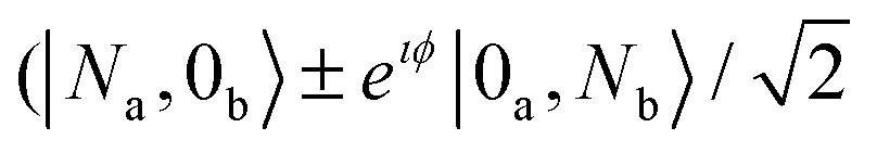 , where ϕ is the relative phase between the two-mode states. Such states can be useful for super-resolution phase measurements and quantum metrological applications.27
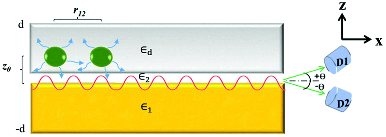 | ||
| Fig. 1 Schematic of the proposed architecture having a metal film separated from a dielectric film embedded with quantum dots. The dielectric constants of the metal, dielectric and the layer between them are given by, ε1, εd, and ε2, respectively. The separation between the two QDs and that between the QDs and metal film are given by r12, and z0, respectively. The emitted path-entangled states can be measured by the detectors labeled D1 and D2. | ||
The structure of this paper is as follows: in section 2, we describe the model with all relevant Hamiltonian and calculation of the intensity pattern at the output. Next, we discuss in section 3 how such a pattern refers to a non-classical correlation between the emitted photons. We analyze our results in section 4 followed by the scope and limitations of the present proposal. Finally, we conclude the paper in section 5.
2. Model
Let us start our analysis with two identical dipole emitters, at a distance r12 from each other, placed very close to a metal–dielectric interface at a fixed distance z0(>0) (see Fig. 1). Each emitter can be considered as a two-level system with the relevant energy levels |g〉 and |e〉, the transition frequency ω0, and the dipole moment d.28 Two detectors D1 and D2 are placed in the far-field region at the end of the interface to detect the photons that are radiated from the emitters.Note that the coupling of the dipole emitters with the SP mode depends on the location and orientation of the emitters.23 We first assume that both the emitters have the dipole moments oriented in the same direction say perpendicular to the interface (i.e., along z-axis), and are initially in their respective excited states. The decay rate of these gets modified to a value larger than that in free space in the vicinity of the metal surface. The total decay rate of each emitter can have contributions from various decay channels, e.g., through the SP mode, into the radiative modes and various non-radiative modes including dissipation in metals. At a moderate distance from the interface, the decay of the emitters is dominated primarily into the SP mode over other channels.29 To this end, we model this decay into the SP mode as a strong coherent coupling between emitters and the SP mode. The other decay channels however are treated as the standard Markovian dissipation mechanism.
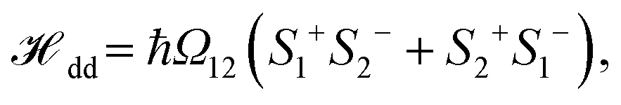
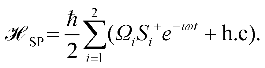
The Hamiltonian of the joint system comprising the emitters and the SP mode then can be written as30
 | (1) |
 | (2) |
 | (3) |
 | (4) |
Here Si+ and Si− are the energy raising and lowering operators for the ith emitter with the transition frequency ω0, ħΩ12 is the dipole–dipole interaction energy which can be represented by the corresponding Green's function29,31 and Ωi is the Rabi frequency of the ith emitter, when driven by the electromagnetic field E in the SP mode. This can be written as Ωi = di·E/ħ, where the field E is given by 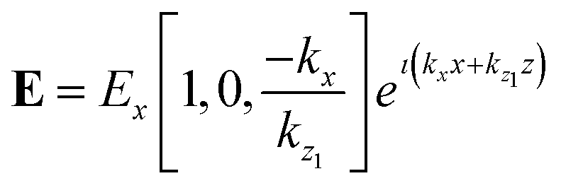 . Here the wave vector of the field along the x-direction is given by
 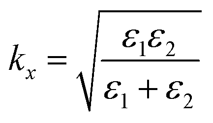 , where ε1 and ε2 are the permittivities of the metal (z < 0) and the dielectric (z > 0), respectively. The wave-vector
  (k0 being the wave vector in free space) in the z-direction is imaginary in both the media and represents a decaying amplitude along the z-direction (i.e., perpendicular to the interface). Here we emphasize that the SP mode is treated classically unlike in other relevant studies.23,32,33
The SP field suffers from the propagation loss along the +x direction. The amplitude of N photons in the SP mode gets reduced by a factor of exp(−N2D/LSP) through a distance D, where LSP is the propagation length scale.34 The photons come out at the end of the interface (x = 0, z = 0) into free space (i.e., radiative) modes with a finite probability of transmission across the interface boundary. Considering the propagation loss, the transmission probability into the free space modes can be calculated as large as ∼0.54 for (D = 1 μm and LSP = 19 μm) across all possible modes24 (see the ESI† for the calculation of transmission). We have chosen the permittivity ε2 of the dielectric close to unity. Henceforth, in the rest of this paper, we choose an air–metal interface, such that ε2 = 1.23 In such a configuration, it would also become convenient to use lasers to initially excite the emitters.
At the end of the interface, the angular distribution of the scattered intensity in the far-field is given by35
 | (5) |
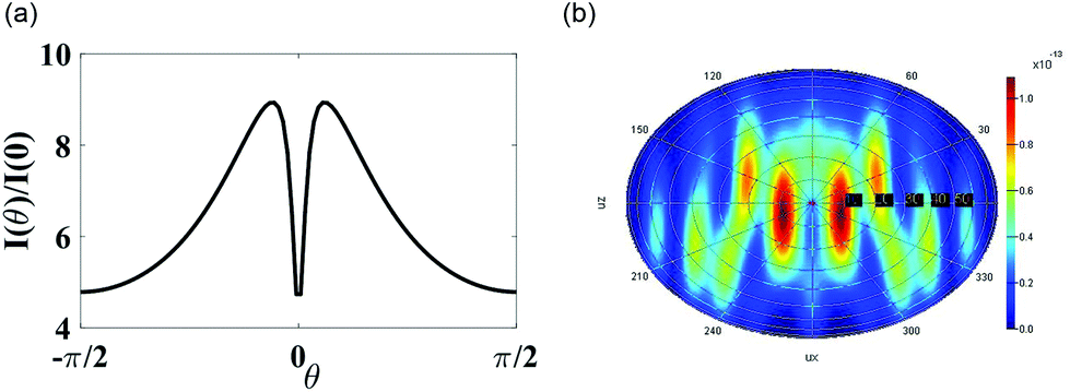 | ||
| Fig. 2 (a) Far-field angular distribution of the field scattered at the end of the interface for ε1 = −9.23 + 0.3ı and ε2 = 1, λ0 = 490 nm, λSP = 0.94λ0. Here θ0 is found to be 0.18 radians; (b) FDTD simulations depicting the far-field angular distribution of the intensity of transmitted free space radiation from the end of the interface. | ||
To verify the results, finite difference time domain (FDTD) simulations of the proposed structure (Fig. 1) were carried out with 2 dielectric emitters embedded in a 100 nm thick dielectric layer (details are provided in the ESI†) that shows the two beams coming out from the interface (see Fig. 2b). We performed simulations on the structures for different cases such that in-plane dimensions are within LSP. More importantly, even after considering losses in the system two peak patterns are observed in the far field region as predicted in Fig. 2a.
3. Intensity–intensity correlation
As the two emitters interact directly with each other and cross-talk through their common interaction with the same SP mode, there would exist a correlation between the photons emitted by them. Such a correlation between these photons could be indicated when detected at the detectors D1 at position R1 and D2 at R2 in the far-field regime. These two detectors would only detect the number of photons, irrespective of their polarization. We have calculated the intensity-intensity correlation of the field emitted from both the emitters, at the end of the interface by placing two detectors as shown in Fig. 1. The correlation of the electromagnetic field can be represented in terms of the second-order correlation function29,30 of spin operators of each two-level dipole emitter, as follows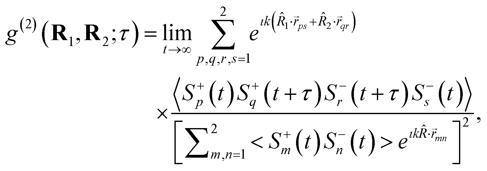 | (6) |
Here, we have calculated the expectation values of the higher-order combinations of spin operators using the quantum regression theorem36 and the solutions of the following master equation of the density matrix ρ of the two emitters:
 | (7) |
4. Results and discussion
In Fig. 3(a), we display the behavior of the second-order correlation function g(2)(τ). We found that g(2)(0) = 0, which signifies that both the detectors D1 and D2 do not click simultaneously – in other words, both the photons reach at either detector at the same time, but not at two different detectors. This is a clear signature of coalescence of photons, which would therefore follow sub-Poissonian statistics, indicating non-classical behaviour of the photons. This result is similar to that obtained in the Hong-Ou-Mandel effect,37 in which one measures the second-order correlation of two optical beams at two detectors. Moreover, such a behaviour persists for all values of dipole–dipole coupling strength Ω12, which is a function of r12, the distance between the emitters. This signifies that the time of emission of the photons from the emitters and the path difference r12 while reaching at the detectors do not play any role in the photon statistics.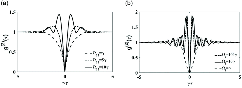 | ||
| Fig. 3 (a) Second order correlation function for different interaction energies Ω12 between the emitters. We have chosen Ωi = γ,i ∈ 1,2; (b) second order correlation function for different coupling strengths Ωi. We use Ω12 = γ and considered all Ωi values to be equal. | ||
In Fig. 3(b), we present the variation of the second order correlation function for different coupling strengths Ωi, where we have assumed γij = γid = γ(i,j ∈ 1,2). For small coupling (Ωi ≲ γ), we find that g(2)(τ ≠ 0) increases monotonically from zero to 1. On the other hand, for large coupling Ωi ≫ γ, the correlation function oscillates with τ that arises due to Rabi coupling between the emitters and SP mode. For very large τ (≫1/γ), g(2)(τ) approaches 1, signifying a Poissonian statistics, similar to that for a coherent state. Most importantly, g(2)(0) remains zero irrespective of the value of Ωi, i.e., the non-classical behaviour of photons persists for all Ωi values.
4.1. Experimental feasibility
Our model can be realized on a silver-air interface where the dielectric constant for silver is ε1 = −9.23 + 0.3ı at wavelength λ0 = 490 nm (λSP = 0.94λ0)38 and that for air ε2 = 1, with the corresponding propagation length of surface plasmon mode LSP ∼ 19 μm (≫λSP) and the evanescent decay of the SP mode along the z-direction is ∼224 nm into the dielectric.39,40 One can maintain a constant distance z0 between the emitters and the interface using a few nanometer spacer layer with the dielectric constant close to unity.23 We choose γ = 2.9 × 10⁹ Hz for numerical simulations. The proposed scheme can be tested with the metal coated on one substrate that is fixed and the dielectric layer with embedded emitters on another substrate that is mounted on a piezo stage. The piezo stage can help control the spacing and thus the coupling strength. A similar experiment with two prisms was reported earlier.41 This will ensure the air gap needed for maximum coupling. An alternate scheme is to have a multi-layer stack with a metal, a porous material that is glancing angle deposited (porous alumina, for example) and a dielectric layer with emitters. A refractive index of 1.025 was reported for porous alumina.42In our model we considered so far that the emitters are identical in size and orientation. It is noted that such uniformity can be achieved in colloidal quantum dots. For example, CdSe, CdS, PbSe, PbS, etc., are commercially available within a 1% variation in size (in respective wavelength also). Furthermore, we assumed that the dipole moments of the emitters are oriented perpendicular to the interface so as to maximize the coupling with the SP field (see Fig. 12.2 (ref. 29)). However, for random orientation of these emitters one could take an isotropic average of the orientation of dipole moment such that the effective Rabi coupling becomes 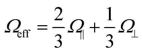 (where Ω∥,⊥ refers to the Rabi coupling for parallel and perpendicular orientation of the dipole moment with respect to the interface23). It would certainly reduce the coupling, i.e., Ωeff < Ω⊥. As noted in Fig. 3, this however does not change our result g(2)(0) = 0, which is valid for all values of Ωi. We also emphasize that in our analysis, we have incorporated all possible sources of decoherence of emitters in eqn (7). This includes decay into radiative and non-radiative channels and also the individual dephasing of the emitters.
4.2. Implications
The coalescence behaviour indicates that the photons are detected at the states |2,0〉 or |0,2〉 with equal probability, where |n,m〉 refers to a situation with n photons detected at the detector D1 and m photons at D2. This is irrespective of the radiative modes that the photons have been emitted into. This, therefore, indicates the formation of a path-entangled state of the two photons: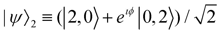 . The relative phase ϕ is washed out upon detection; however, it could be measured using homodyne detection techniques. It must be borne in mind that the two possible paths of photons exhibit angular symmetry and the above state is therefore immune to any dephasing that could arise from path-difference. Note further that entangled photons can travel a long distance in free space (as demonstrated in free-space quantum communication experiments43) before attenuation. Therefore, the decay of emitted photons traveling in the free space to the detector can be considered negligible in the present case.
From the above discussion it is clear that, if not detected, the emitted photons are prepared in the state |ψ〉2, which is a N00N-like state. The same architecture could also generate a state like  , if one would use N emitters, all initially excited. These photons, once radiated out, can therefore be used for further applications. In a similar way, if one detects no photon in one of the directions of photon emission then there would be N photons in the other direction of emission. These photons could also be coupled into further sets of metal–dielectric interfaces (see Fig. 4). This makes our model a plausible plasmonics-based architecture for quantum information processing.
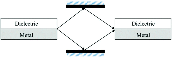 | ||
| Fig. 4 A possible architecture for long-distance quantum information processing. The photons emitted from one interface can be fed into another, using mirrors, reminiscent of the end-fire coupling in plasmonic systems.44 In this way, the non-classical properties and entanglement of photons could be transferred to distant interfaces. This would also allow one to build a quantum network (each interface is equivalent to the node of a quantum network) at the nanoscale. | ||
5. Summary
In summary, we have explored possibilities of generating non-classical states of photons using dipole emitters placed on a metal–dielectric interface. We have found that the optically excited SP mode can radiate out of the interface into the radiative modes and exhibit non-classical properties, namely, photon coalescence. This indicates that these photons are prepared in N00N-like path-entangled states and therefore could be used for metrology. Our proposed architecture has the potential as a building block of plasmonics-based quantum information processing.Conflicts of interest
There are no conflicts to declare.Acknowledgements
The authors sincerely acknowledge fruitful discussion with Prof. S. Dutta Gupta and Dr Rajesh V. Nair during the early stage of this work. The authors also thank Dr Asoka Biswas for critical reading of the manuscript. One of us (S. D.) acknowledges the financial support from DST-SERB, Government of India (project no. CRG/2018/003574) during this work.References
- H. J. Kimble, Nature, 2008, 453, 1023–1030 CrossRef CAS PubMed; C. Morneo and J. Kim, Science, 2013, 339, 1164–1169 CrossRef PubMed; J. Yin, et al. , Science, 2017, 356, 1140–1144 CrossRef PubMed.
- I. A. Walmsley and M. G. Raymer, Science, 2005, 307(5716), 1733–1734 CrossRef CAS PubMed; C. Monroe, Nature, 2002, 416, 238–246 CrossRef PubMed.
- H. Weinfurter, Photons, Adv. At., Mol., Opt. Phys., 2008, 42(2000), 489–533 Search PubMed; A. Zeilinger, Phys. Scr., 2017, 92, 072501 CrossRef.
- J. T. Barreiro, T. C. Wei and P. G. Kwiat, Nat. Phys., 2008, 4, 282–286 Search PubMed; E. Waks, A. Zeevi and Y. Yamamoto, Phys. Rep., 2010, 497(1), 1–40 CrossRef.
- S. L. Braunstein and P. Loock, Rev. Mod. Phys., 2005, 77, 513–517 CrossRef.
- A. Furusawa, J. L. Sørensen, S. L. Braunstein, C. A. Fuchs, H. J. Kimble and E. S. Polzik, Science, 1998, 282, 706–709 CrossRef CAS PubMed.
- M. O. Scully and M. S. Zubairy, Quantum Optics, Cambridge University Press, Cambridge, 1997 Search PubMed.
- A. Ling, A. Linares and C. Kurtsiefer, Phys. Rev. A: At., Mol., Opt. Phys., 2008, 77, 043834 CrossRef.
- H. Terashima, et al. , Sci. Rep., 2018, 8, 15733 CrossRef.
- K. D. Jöns, et al. , J. Phys. D: Appl. Phys., 2015, 48, 085101 CrossRef CAS; W. B. Gao, A. Imamoglu, H. Bernien and R. Hanson, Nat. Photonics, 2015, 9, 363 CrossRef; I. J. Luxmoore, et al. , Phys. Rev. Lett., 2013, 110, 037402 CrossRef PubMed; P. Lodahl, S. Mahmoodian and S. Stobbe, Rev. Mod. Phys., 2015, 87, 347 CrossRef; A. Orieux, et al. , Rep. Prog. Phys., 2017, 80, 076001 CrossRef PubMed; H. Siampour, S. Kumar and S. I. Bozhevolny, ACS Photonics, 2017, 4(8), 1879 CrossRef.
- M. Tame, et al. , Phys. Rev. Lett., 2008, 101, 190504 CrossRef CAS PubMed.
- P. Anger, P. Bharadwaj and L. Novotny, Phys. Rev. Lett., 2006, 96, 113002 CrossRef; S. Kühn, U. Høakanson, L. Rogobete and V. Sandoghdhar, Phys. Rev. Lett., 2006, 97, 017402 CrossRef PubMed.
- D. E. Chang, A. S. Sorensen, P. R. hemmer and M. D. Lukin, Phys. Rev. Lett., 2006, 97, 053002 CrossRef CAS PubMed.
- A. V. Akimov, et al. , Nature, 2007, 450, 402 CrossRef CAS PubMed.
- F. Le Kien and K. Hakuta, Phys. Rev. A: At., Mol., Opt. Phys., 2008, 77, 033826 CrossRef.
- R. W. Heeres, L. P. Kouwenhoven and V. Zwiller, Nat. Nanotechnol., 2013, 8, 719 CrossRef CAS PubMed; G. DiMartino, et al. , Phys. Rev. Appl., 2014, 1, 034004 CrossRef; Y. J. Cai, et al. , Phys. Rev. Appl., 2014, 2, 014004 CrossRef.
- G. Fujii, D. Fukuda and S. Inoue, Phys. Rev. B: Condens. Matter Mater. Phys., 2014, 90, 085430 CrossRef CAS; J. S. Fakonas, H. Lee, Y. A. Kelaita and H. A. Atwater, Nat. Photonics, 2014, 8, 317 CrossRef.
- B. Vest, et al. , Science, 2017, 356, 1373 CrossRef CAS PubMed.
- J. S. Fakonas, A. Mitskovets and H. A. Atwater, New J. Phys., 2015, 17, 023002 CrossRef.
- M.-C. Dheur, et al. , Phys. Rev. B, 2017, 96, 045432 CrossRef.
- A. Huck, et al. , Phys. Rev. Lett., 2009, 102, 246802 CrossRef PubMed.
- A. Huck and U. L. Andersen, Nanophotonics, 2016, 5, 3483 Search PubMed.
- A. Gonzalez-Tudela, P. A. Huidobro, L. Martin-Moreno, C. Tejedor and F. J. Garcia-Vidal, Phys. Rev. Lett., 2013, 110, 126801 CrossRef CAS PubMed.
- A. A. Maradudin, R. F. Wallis and G. I. Stegeman, Prog. Surf. Sci., 1990, 33, 171 CrossRef CAS.
- D. E. Chang, A. S. Sorensen, E. A. Demler and M. D. Lukin, Nat. Phys., 2007, 3, 807–812 Search PubMed.
- M. W. Mitchell, J. S. Lundeen and A. M. Steinberg, Nature, 2004, 429, 161–164 CrossRef CAS PubMed; A. N. Boto, et al. , Phys. Rev. Lett., 2000, 85, 2733 CrossRef PubMed.
- J. P. Dowling, Contemp. Phys., 2008, 49, 125 CrossRef CAS; M. A. Taylor and W. P. Bowen, Phys. Rep., 2016, 615, 1 CrossRef; H. Zang, et al. , Nat. Photonics, 2011, 5, 628 CrossRef.
- A. Zrenner, et al. , Nature, 2002, 418, 612 CrossRef CAS PubMed; A. J. Ramsay, et al. , Phys. Rev. Lett., 2008, 100, 197401 CrossRef PubMed; H. Kamada, et al. , Phys. Rev. Lett., 2001, 87, 24 CrossRef PubMed; H. Htoon, et al. , Phys. Rev. Lett., 2002, 88, 8 CrossRef PubMed.
- A. A. Maradudin, J. Roy Sambles and W. L. Barnes, Modern Plasmonics, Elsevier, USA, 2014 Search PubMed.
- J.-T. Chang, J. Evers and M. S. Zubairy, Phys. Rev. A: At., Mol., Opt. Phys., 2006, 74, 043820 CrossRef.
- Ho. Dung, L. Knoll and D. Welsch, Phys. Rev. A: At., Mol., Opt. Phys., 2002, 66, 063810 CrossRef.
- A. Archambault, F. Marquier and J. Greffet, Phys. Rev. B: Condens. Matter Mater. Phys., 2010, 82, 035411 CrossRef.
- C. E. Susa, J. H. Reina and R. Hildner, Phys. Rev. A: At., Mol., Opt. Phys., 2014, 378, 2371 CAS.
- B. Vest, et al. , New J. Phys., 2018, 20, 053050 CrossRef.
- H. Hu, X. Zeng, D. Ji, L. Zhu and Q. Gan, J. Appl. Phys., 2013, 113, 053101 CrossRef.
- H. J. Carmichael, Statistical Methods in Quantum Optics 1, Springer, New York, 1999 Search PubMed.
- C. K. Hong, Z. Y. Ou and L. Mandel, Phys. Rev. Lett., 1987, 59, 2044 CrossRef CAS PubMed.
- P. B. Johnson and R. W. Christy, Phys. Rev. B: Solid State, 1972, 6, 4370 CrossRef CAS.
- S. A. Maier, Plasmonics Fundamentals and Applications, Springer, New York, 2010 Search PubMed.
- H. Raether, Surface Plasmons on Smooth and Rough Surfaces and on Gratings, Springer-Verlag, Berlin, 1988 Search PubMed.
- K. R. Welford and J. R. Sambles, J. Mod. Opt., 1988, 35, 1467 CrossRef CAS; M. Balasubrahmaniyam, et al. , Appl. Phys. Lett., 2017, 110, 171101 CrossRef.
- Xu A. Zhang, et al. , Adv. Funct. Mater., 2015, 25, 6644 CrossRef CAS.
- N. Gisin, et al. , Rev. Mod. Phys., 2002, 74, 145 CrossRef; R. J. Hughes, New J. Phys., 2002, 4, 43 CrossRef.
- C. Fisher, et al. , J. Opt. Soc. Am. B, 2015, 32, 412 CrossRef CAS.
Footnote |
| † Electronic supplementary information (ESI) available. See DOI: 10.1039/C9NR06529F |
| This journal is © The Royal Society of Chemistry 2020 |