DOI:
10.1039/C9NJ04796D
(Paper)
New J. Chem., 2020,
44, 64-71
CdS structures prepared in AAO nanochannels via different synthesis methods under limited conditions
Received
20th September 2019
, Accepted 30th October 2019
First published on 19th November 2019
Abstract
Nanomaterials have been widely used in the fields of photocatalysis, sensors, and solar cells due to their excellent properties. However, nanomaterials are mainly prepared under nonlimited conditions. With the development of biomimetic nanochannels, their gating properties and chemical stability have come to the fore. Inspired by the potential applications of biomimetic nanochannels, it is significant to synthesize nanomaterials inside biomimetic nanochannels under limited conditions for facilitating newer applications. Therefore, we used an anodic aluminum oxide (AAO) template with different pore diameters as the limited condition to synthesize CdS structures via different synthesis methods. We successfully synthesized CdS nanoparticles and flower-like CdS structures in AAO nanochannels by the electrochemical-assisted method or solution impregnation method. Field-emission scanning electron microscope (FESEM) results revealed that the CdS nanoparticles would agglomerate together to form irregular bulks with an increase in the applied voltage; flower-like CdS structures would block the AAO nanochannels for longer reaction times and higher concentrations. Energy-dispersive spectrometer (EDS) and X-ray diffraction (XRD) results revealed that these structures self-assembled into AAO nanochannels were, in fact, CdS. In conclusion, these methods can provide important guidelines for nanomaterial synthesis in AAO nanochannels.
1. Introduction
With the rapid expansion in the field of nanomaterials, they have exerted a profound impact on people's daily lives. Moreover, nanomaterials have found wide applications in luminescent materials, semiconductor devices, solar cells, drug delivery, sensors, photocatalysis, and other fields because of their excellent physical and chemical properties.1–6 It is well known that living beings have several unique functions because of which scientists have carried out research involving bionic science inspired by such specialized functions. For example, Gu et al. prepared photonic crystal surface materials inspired by the colorful wings of insects;7 Gao et al. synthesized colloidal crystal materials inspired by the compound eye of mosquitoes;8 Zhao et al. formulated multicavity structural materials inspired by polar bear hair;9 and Yu et al. constructed orderly nanomaterials inspired by shellfish.10 The development of biomimetic materials has promoted the living standard of people, as well as had an important application value for human society.
It is well known that the survival of living organisms and their various unique functions are inseparable from the exchange of various substances in their body, which is carried out in ion nanochannels (limited condition). In order to explore the relationship between ion nanochannels and the survival of living organisms, scholars have gradually paid attention to the research on the preparation and application of biomimetic nanochannels. For example, Wen et al. built a voltage-driven chloride ion nanochannel to control the transmission of chloride ions in the nanochannel under the regulation of voltage.11 They also prepared a bioinspired multifunctional heterogeneous membrane with polystyrene-b-poly(4-vinylpyridine) (PS48000-b-P4VP20300) and porous anodic alumina (PAA) membrane,12 as well as porous polyethylene terephthalate (PET) membrane and polystyrene-block-poly(N,N-dimethylaminoethylmethacrylate) (PS14000-b-PDMAEMA3600),13 for highly efficient selective ionic gating. Li et al. synthesized lettuce-like CuxS structures comprising light-responsive 1,3,3-trimethylindolino-6′-nitrobenzopyrylospiran (Spiro) molecules and combined with a porous anodic aluminum oxide (AAO) film to yield specific light-gating heterogeneous nanochannels.14 Xia et al. made different modifications on the surface and inside of AAO nanochannels for the purpose of analyzing the synergistic effect of functional molecules on the inner or outer surfaces of AAO nanochannels.15 On this basis, layered physical deposition was carried out on the inner and outer surfaces of the AAO nanochannels, which realized the spatial division of functional molecules on the outer and inner surfaces.16 Therefore, the specific response of the molecular modification of biomimetic nanochannels can yield intelligent nanochannels with response characteristics toward light, electricity, pH, etc.,17–19 which can have very important applications in the fields of biomolecular response and detection.
As an important II–VI semiconductor with a direct optical bandgap (2.42 eV), CdS has proven to be an outstanding photoelectric semiconductor due to its excellent optical properties and good stability.20,21 There are many potential electronic and photonic applications of CdS nanostructures, such as catalysis,22 photosensors,23 and DNA sensors.24 However, the preparation of CdS is mainly carried out under nonlimited conditions, such as CdS nanowires prepared by the solvent heating method,25 dendritic-like CdS prepared via a hydrothermal method,26 and CdS films prepared by electrodeposition.27 Evidently, researchers have prepared CdS nanowires and CdS nanotubes under limited conditions via the template method, where AAO was used as the template. For example, Mondal et al. studied the optical properties of CdS nanowires prepared by electrodeposition using AAO as the template.28 Yang et al. prepared CdS nanowire arrays by electrodeposition using AAO as the template.29 Wang et al. used AAO as the template to prepare CdS nanotubes and discussed electrochemiluminescence in H2O2 solutions.30 Therefore, it is imperative to investigate CdS nanostructures self-assembled in biomimetic nanochannels under limited conditions inspired by the potential applications of biomimetic nanochannels. Herein, we used the AAO template with different pore diameters as the limited condition to synthesize CdS nanostructures via different synthesis methods. In this work, we successfully synthesized CdS nanoparticles in AAO nanochannels by electrochemical-assisted method, and flower-like CdS structures were obtained in AAO nanochannels via the solution impregnation method at different reaction times.
2. Experimental
2.1 Materials and characterization
The pore diameters of the AAO templates were determined to be 80–100 nm (thickness: 60 μm) and 160–200 nm (thickness: 40 μm) (Pu-Yuan Nano Technology Co., Ltd, Hefei, China). Cadmium nitrate, sodium sulfide, thiourea, hexamethylenetetramine (HMT), and potassium chloride were purchased from Sinopharm Chemical Reagent Co., Ltd. (Beijing, China). 3-Hydroxytyramine hydrochloride (PDA) was purchased from Shanghai Macklin Biochemical Co., Ltd (Shanghai, China). Tris(hydroxymethyl)methyl aminomethane was purchased from Shanghai Aladdin Chemical Reagent Co., Ltd (Shanghai, China). All the chemicals in this work were of the analytical grade and used as received without any further purification; the aqueous solutions were prepared using ultrapure water (18.2 MΩ cm). The morphologies were characterized by a field-emission scanning electron microscope (FESEM, SU8010, Hitachi); subsequently, an energy-dispersive spectrometer (EDS, XFlash 610-H, Bruker) was used to analyze the chemical composition. The crystal phase of the samples was measured by X-ray diffraction (XRD) (D8 ADVANCE XRD, Bruker AXS). The transmissivity of the samples was measured by an ultraviolet-visible spectrophotometer (UV-vis, UV-2600, Shimadzu). The current–voltage curves were measured by a CHI 660E electrochemical workstation (CH Instruments Inc., Shanghai). The Keithley 6487 picoammeter (Keithley Instruments, Cleveland) was used as the power supply.
2.2 Synthesis of CdS structures in AAO nanochannels
Scheme 1: initially, PDA was pumped into the AAO template with a pore diameter of 80–100 nm; then, the AAO template was embedded between two electrolytic chambers. One chamber was filled with Cd(NO3)2 solution (0.1 M) and connected to the positive pole of the power supply, and the other chamber was filled with Na2S solution (0.1 M) and connected to the negative pole of the power supply. In this case, Cd2+ and S2− could transfer to the opposite chamber under the applied electric field. Therefore, Cd2+ and S2− reacted and assembled CdS nanoparticles in the inner walls of the AAO nanochannels. After that, the AAO template was washed with ultrapure water several times and dried in air at 60 °C. In order to determine the influence of the applied voltage on the morphology of CdS nanoparticles in the AAO nanochannels, we changed the applied voltage (0.5, 1.0, 2.0, and 3.0 V) to synthesize CdS nanoparticles for different reaction times. All the samples were marked as AAO + CdS.
Scheme 2: firstly, we prepared the reaction solution with 0.01 M Cd(NO3)2, 0.03 M thiourea, and 0.01 M HMT. Thereafter, we placed the AAO templates in centrifuge tubes along with the reaction solution. We placed the centrifuge tubes in the Eppendorf Thermomixer at a speed of 350 rpm at 25 °C for 12 h. After that, we increased the temperature to 80 °C for undertaking the reaction at different reaction times (0.5, 1.0, 1.5, 2.0, and 3.0 h). Finally, we washed the AAO templates with ultrapure water several times and dried them in air at 60 °C. Further, we changed the concentration of the reaction solution (0.005 M Cd(NO3)2, 0.015 M thiourea, and 0.005 M HMT) to synthesize the CdS nanostructures in AAO nanochannels. Further, all the samples were marked as AAO + CdS.
3. Results and discussion
3.1 FESEM results of Scheme 1
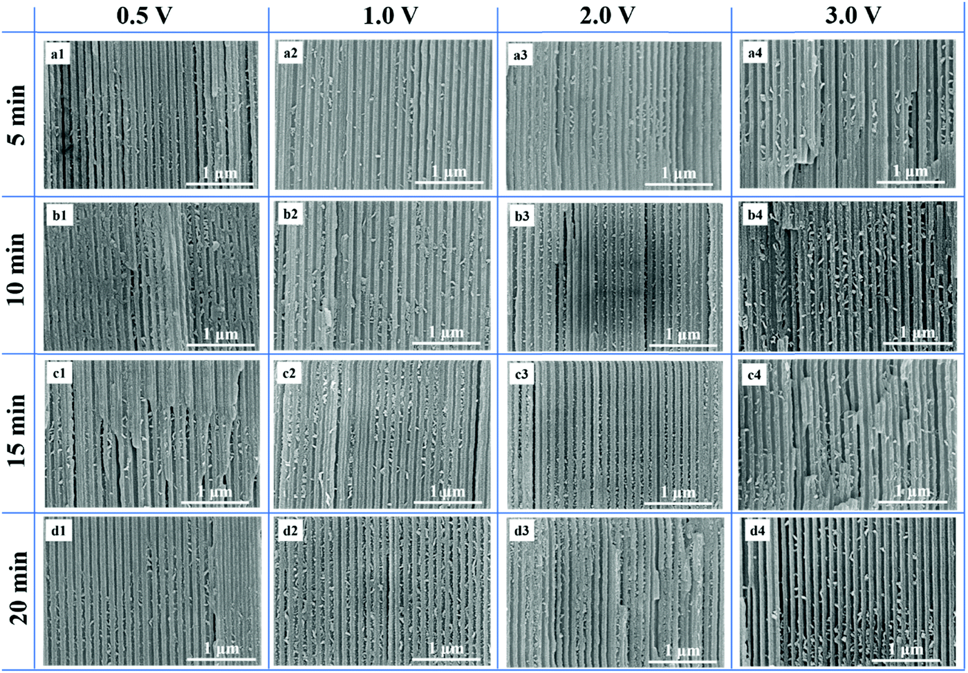
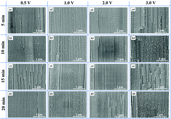
The FESEM results of CdS nanostructures self-assembled in AAO nanochannels (pore diameter: 80–100 nm) under different applied voltages and reaction times are shown in Fig. 1. From Fig. 1(a1), it is evident that a small number of CdS nanoparticles agglomerated in the AAO nanochannels when the applied voltage was 0.5 V and reaction time was 5 min, but the distribution was nonuniform. When the reaction time increased from 10 to 20 min, an increased number of CdS nanoparticles were assembled in the AAO nanochannels and agglomerated to form irregular bulks with a uniform distribution (Fig. 1(b1, c1, d1)). This implies that more CdS nanoparticles were dispersed in AAO nanochannels with an increase in the reaction time. In order to further explore the influence of applied voltage on CdS nanostructures self-assembled in AAO nanochannels, we changed the applied voltage to synthesize CdS nanostructures in AAO nanochannels. From Fig. 1(a1–a4), it is evident that an increased number of CdS nanoparticles assembled in the AAO nanochannels as the applied voltage increased from 0.5 to 3.0 V for a reaction time of 5 min. Moreover, AAO nanochannels were blocked by CdS nanoparticles under higher applied voltages and reaction times. Fig. 1 shows the confirmation that when the applied voltage is gradually increased, the movement speeds of Cd2+ and S2− become faster and the reaction becomes drastic. Moreover, CdS nanoparticles agglomerated to form irregular bulks at higher applied voltages under the adhesion of PDA polymer films.31
 |
| | Fig. 1 FESEM images of AAO + CdS at different applied voltages and reaction times. | |
3.2 EDS results of Scheme 1
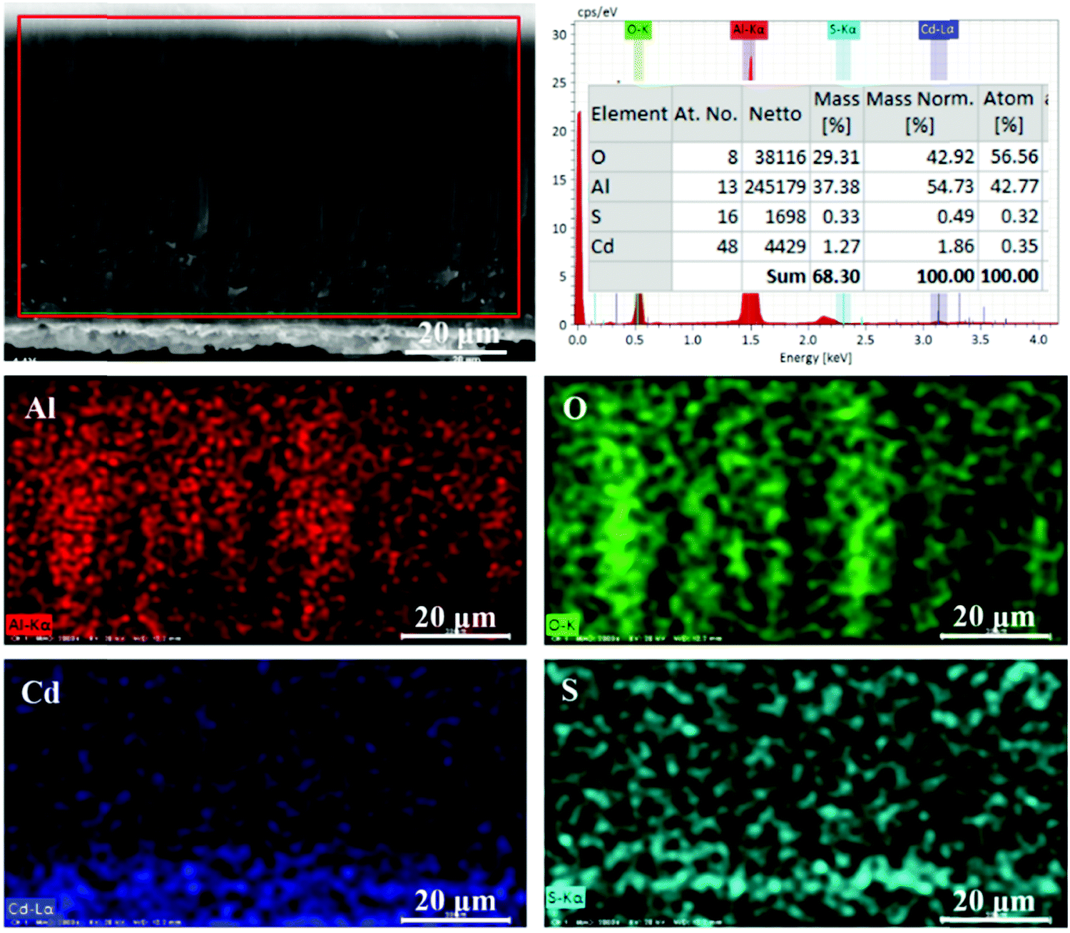
The elemental composition analysis of the AAO + CdS sample was carried out when the applied voltage was 1.0 V and reaction time was 15 min. The EDS results are shown in Fig. 2. From the elemental mapping results (Fig. 2), it is evident that the sample mainly comprises elemental Al, O, Cd, and S. The elemental composition of the AAO template is relatively high, but the contents of elemental Cd and S were relatively low. The wt% values of elemental Cd and S were 1.86% and 0.49%, respectively, and the atomic ratio of Cd![[thin space (1/6-em)]](https://www.rsc.org/images/entities/char_2009.gif) :S was 0.35:0.32; this indicated that CdS nanostructures were successfully assembled in the AAO nanochannels.
:S was 0.35:0.32; this indicated that CdS nanostructures were successfully assembled in the AAO nanochannels.
 |
| | Fig. 2 EDS result of CdS self-assembled in AAO nanochannels. | |
3.3 UV-vis transmissivity results of Scheme 1
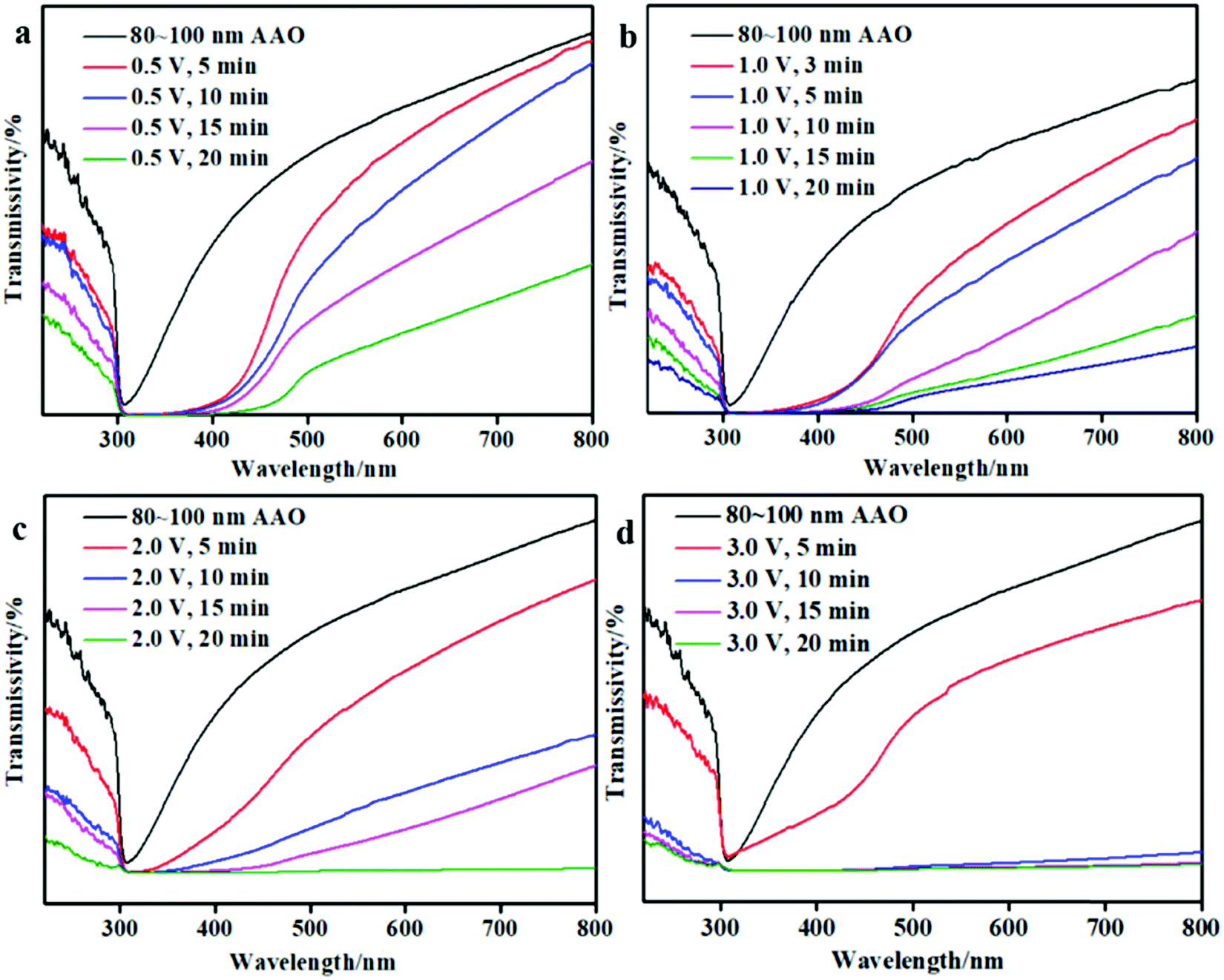
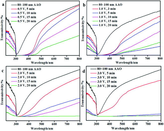
The UV-vis transmissivity results of the AAO + CdS samples under different reaction conditions are shown in Fig. 3. From Fig. 3(a), it is clear that the transmissivity of the AAO + CdS sample decreases when the wavelength is 500 nm with an increase in the reaction time when the applied voltage is 0.5 V. Similarly, from Fig. 3(b, c, d), it is evident that the transmissivity of the AAO + CdS sample gradually decreased with an increase in the applied voltage and reaction time. When combined with the FESEM results, it is clear that an increased number of CdS nanoparticles agglomerated together to form irregular blocks with an increase in the applied voltage, which is adverse for light transmission and reduces the transmissivity of the AAO + CdS sample. Therefore, the applied voltage cannot be excessively high.
 |
| | Fig. 3 Optical transmission spectrums of the AAO + CdS sample under different reaction conditions. | |
3.4
I–V curves of Scheme 1
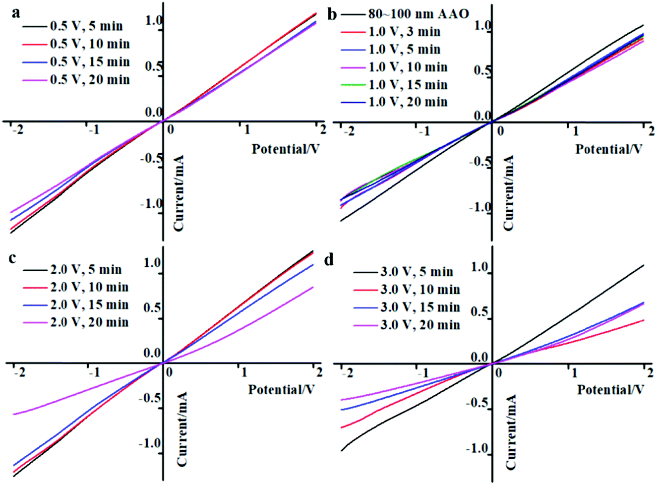
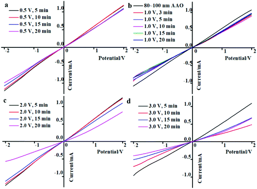
The I–V curves of the AAO + CdS samples under different reaction conditions are shown in Fig. 4. From Fig. 4(a), it is clear that the ionic current obviously declined when the reaction time was increased from 5 to 20 min at an applied voltage of 0.5 V. As shown in Fig. 4(b), the ionic current of the AAO + CdS samples at different reaction times exhibit a marginal difference when the applied voltage increased to 1.0 V, but all of them are smaller than those of pure AAO nanochannels. However, the ionic current of the AAO + CdS samples began to significantly change when the applied voltage increased from 2.0 and 3.0 V for different reaction times. This is consistent with the UV-vis transmissivity results. Therefore, the higher density of CdS nanoparticles assembled in the AAO nanochannels yielded AAO nanochannels with higher steric resistance under higher applied voltages, which makes it difficult for ions to pass through AAO nanochannels.
 |
| | Fig. 4
I–V curves of the AAO + CdS sample under different reaction conditions. | |
3.5 FESEM results of Scheme 2
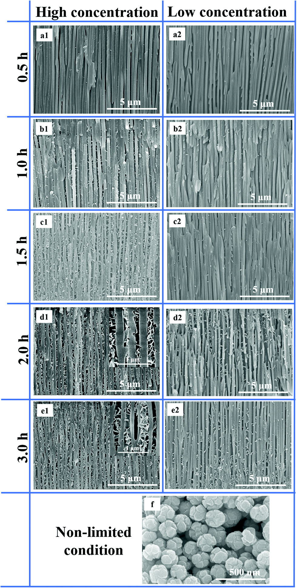
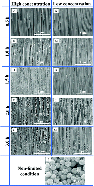
The FESEM results of the CdS nanostructures self-assembled in AAO nanochannels (pore diameter: 160–200 nm) via the solution impregnation method at different concentrations and reaction times are shown in Fig. 5. From Fig. 5(a1), it is evident that there were a few CdS nanostructures in the AAO nanochannels when the reaction time was 0.5 h at higher concentrations. As the reaction time increased to 1 h, we can see the presence of certain CdS nanosheets appearing in the AAO nanochannels (Fig. 5(b1)). When the reaction time increased to 1.5 h, a large number of flower-like CdS structures were assembled in the AAO nanochannels (Fig. 5(c1)). As the reaction time continues to increase from 2 to 3 h, it is evident from Fig. 5(d1, e1) that the AAO nanochannels were closely stacked with flower-like CdS nanostructures. We decreased the concentration of the reaction solution in order to synthesize CdS nanostructures in AAO nanochannels according to the above method. As shown in Fig. 5(a2), we cannot see any CdS nanostructures in the AAO nanochannels. From Fig. 5(b2, c2), it is evident that there were a few CdS nanostructures in the AAO nanochannels when the reaction time was 1.0 and 1.5 h. When the reaction time increased from 2 to 3 h, a few CdS nanosheets staggered together to form flower-like structures were visible (Fig. 5(d2, e2)). However, when we synthesized CdS nanostructures under nonlimited conditions at the same concentration of reaction solution, the morphology of CdS is a nanosphere (Fig. 5(f)). Therefore, from Fig. 5, we can confirm that the limited condition has an obvious impact on the morphology of CdS structures.
 |
| | Fig. 5 FESEM images of the AAO + CdS sample for different concentrations and reaction times. | |
3.6 EDS and XRD results of Scheme 2
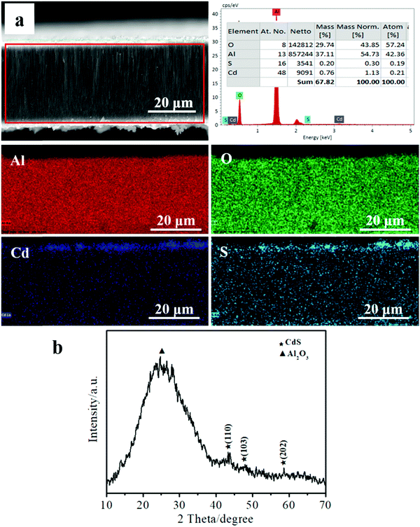
The elemental composition analysis and XRD pattern of the sample (as shown in Fig. 5(e2)) were determined, and the results are shown in Fig. 6. From the elemental mapping results shown in Fig. 6(a), it is clear that the sample mainly contains elemental Al, O, Cd, and S. However, the contents of elemental Cd and S were relatively low. The wt% values of elemental Cd and S were 1.13% and 0.30%, respectively, and the atomic ratio of Cd:S was 0.21:0.19. As shown in Fig. 6(b), the obvious diffraction peak was effectively indexed to Al2O3. Further, we can find three inconspicuous peaks effectively indexed to the hexagonal phase of CdS. These results reveal that the flower-like structures were, in fact, CdS.
 |
| | Fig. 6 (a) EDS and (b) XRD results of CdS self-assembled in the AAO nanochannels. | |
3.7 UV-vis transmissivity results of Scheme 2
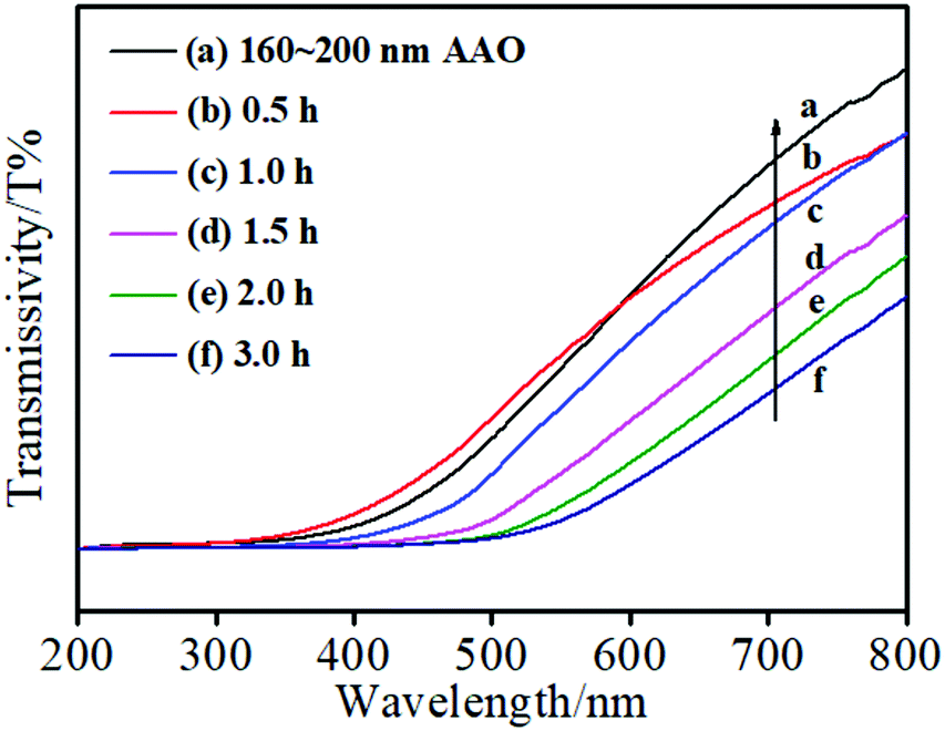
The UV-vis transmissivity results of the AAO + CdS samples (as shown in Fig. 6(a1–d1)) at different reaction times are shown in Fig. 7. Evidently, with an increase in reaction time, the transmissivity of the AAO + CdS sample gradually decreased. This is because an increased number of CdS nanostructures assembled in the AAO nanochannels and blocked the AAO nanochannels. The flower-like CdS nanostructures in the AAO nanochannels can hinder the passage of light through the AAO template, resulting in lower transmissivity. In addition, the transmissivity of the AAO + CdS sample started to decline at 520 nm because CdS exhibits strong absorption in the range from 200 to 520 nm. This implies that CdS nanostructures were assembled in the AAO nanochannels.
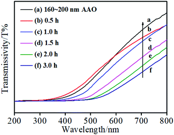 |
| | Fig. 7 Optical transmission spectrums of the AAO + CdS sample for different reaction times. | |
3.8
I–V curves of Scheme 2
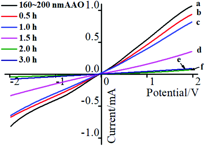
The I–V curves of the AAO + CdS samples (as shown in Fig. 6(a1–d1)) at different reaction times are shown in Fig. 8. From Fig. 8, it is evident that the ionic current obviously declined when the reaction time increased from 0.5 to 3 h. This is consistent with the UV-vis transmissivity results of the AAO + CdS samples. The higher density of the flower-like CdS structures assembled in the AAO nanochannels can block the AAO nanochannels, which makes it difficult for ions to pass through the AAO nanochannels. Therefore, in order to have an obvious ion current signal of the I–V curves, the optimal reaction time of the flower-like CdS self-assembled in AAO nanochannels was determined to be 1.5 h.
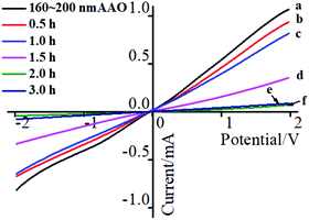 |
| | Fig. 8
I–V curves of the AAO + CdS sample for different reaction times. | |
4. Conclusions
In summary, we successfully synthesized CdS nanoparticles in AAO nanochannels by an electrochemical-assisted method. The FESEM results show that more CdS nanoparticles would form in the AAO nanochannels with an increase in the applied voltage. Some CdS nanoparticles even agglomerated under the adhesion of PDA polymer films. Further, the EDS results revealed that the nanoparticles self-assembled in the AAO nanochannels were, in fact, CdS. The UV-vis transmissivity results and I–V curves obviously declined with an increase in the applied voltage and reaction time. On the other hand, we used the solution impregnation method to prepare CdS nanostructures in the AAO nanochannels. Further, we successfully synthesized flower-like CdS in the AAO nanochannels at higher concentrations according to the FESEM results. The EDS and XRD results revealed that these flower-like structures were CdS nanostructures. The UV-vis transmissivity results and I–V curves obviously declined with an increase in the reaction time. Therefore, these results may provide important guidelines for synthesizing CdS nanostructures in AAO nanochannels.
Conflicts of interest
There are no conflicts to declare.
Acknowledgements
This work was supported by the Scientific Research Foundation for Doctor, Nanning Normal University (No. 602021239253), Open Research Topic for Engineering Research Center of Nano-Geomaterials of Ministry of Education of China University of Geosciences (No. NGM2018KF019). The financial support was gratefully appreciated.
References
- J. Wang, Q. Ma, W. Zheng, H. Liu, C. Yin, F. Wang, X. Chen, Q. Yuan and W. Tan, One-dimensional luminous nanorods featuring tunable persistent luminescence for autofluorescence-free biosensing, ACS Nano, 2017, 11, 8185–8191 CrossRef CAS.
- P. Kumar, E. Vahidzadeh, U. K. Thakur, P. Kar, K. M. Alam, A. Goswami, N. Mahdi, K. Cui, G. M. Bernard and V. K. Michaelis, C3N5: A low bandgap semiconductor containing an azo-linked carbon nitride framework for photocatalytic, photovoltaic and adsorbent applications, J. Am. Chem. Soc., 2019, 141, 5415–5436 CrossRef CAS.
- J. L. Stein, E. A. Mader and B. M. Cossairt, Luminescent InP quantum dots with tunable emission by post-synthetic modification with Lewis acids, J. Phys. Chem. Lett., 2016, 7, 1315–1320 CrossRef CAS.
- C. C. Nascimento, G. R. S. Andrade, O. S. Santos, E. T. Neto, S. S. L. Costa and I. F. Gimenez, Biosilica from diatomaceous earth as support to CdS-mediated photocatalysis in dry and aqueous phase, Mater. Design, 2017, 127, 8–14 CrossRef CAS.
- A. Dey, P. Karan, A. Sengupta, S. A. Moyez, P. Sarkar, S. B. Majumder, D. Pradhan and S. Roy, Enhanced charge carrier generation by dielectric nanomaterials for quantum dots solar cells based on CdS-TiO2 photoanode, Sol. Energy, 2017, 158, 83–88 CrossRef CAS.
- W. J. Han, L. Ren, Z. Zhang, X. Qi, Y. D. Liu, Z. Y. Huang and J. X. Zhong, Graphene-supported flocculent-like TiO2 nanostructures for enhanced photoelectrochemical activity and photodegradation performance, Ceram. Int., 2015, 41, 7471–7477 CrossRef CAS.
- Z. Z. Gu, H. Uetsuka, K. Takahashi, R. Nakajima, A. Fujishima and O. Sato, Structural color and the lotus effect, Angew. Chem., Int. Ed., 2003, 42, 894–897 CrossRef CAS.
- X. F. Gao, X. Yan, X. Yao, L. Xu, K. Zhang, J. M. Zhang, B. Yang and L. Jiang, The dry-style antifogging properties of mosquito compound eyes and artificial analogues prepared by soft lithography, Adv. Mater., 2007, 19, 2213–2217 CrossRef CAS.
- Y. Zhao, X. Y. Cao and L. Jiang, Bio-mimic multichannel microtubes by a facile method, J. Am. Chem. Soc., 2007, 129, 764–765 CrossRef CAS.
- S. H. Yu, M. Antonietti, H. Cölfen and M. Giersig, Synthesis of very thin 1D and 2D CdWO4 nanoparticles with improved fluorescence behavior by polymer-controlled crystallization, Angew. Chem., Int. Ed., 2002, 41, 2356–2360 CrossRef CAS.
- Q. Liu, L. P. Wen, K. Xiao, H. Lu, Z. Zhang, G. H. Xie, X. Y. Kong, Z. S. Bo. and L. Jiang, A biomimetic voltage-gated chloride nanochannel, Adv. Mater., 2016, 28, 3181–3186 CrossRef CAS.
- Z. Zhang, X. Y. Kong, K. Xiao, G. H. Xie, Q. Liu, Y. Tian, H. C. Zhang, J. Ma, L. P. Wen and L. Jiang, A bioinspired multifunctional heterogeneous membrane with ultrahigh ionic rectification and highly efficient selective ionic gating, Adv. Mater., 2016, 28, 144–150 CrossRef CAS.
- Z. Zhang, G. H. Xie, K. Xiao, X. Y. Kong, P. Li, Y. Tian and L. P. Wen, Asymmetric multifunctional heterogeneous membranes for pH- and temperature-cooperative smart ion transport modulation, Adv. Mater., 2016, 28, 9613–9619 CrossRef CAS.
- H. Wang, Q. Liu, W. H. Li, D. Zheng, Z. S. Bo and L. Jiang, Colloidal synthesis of lettuce-like copper sulfide for light-gating heterogeneous nanochannels, ACS Nano, 2016, 10, 3606–3613 CrossRef CAS.
- X. C. Li, T. Y. Zhai, P. C. Gao, H. L. Cheng, R. Z. Hou, X. D. Lou and F. Xia, Role of outer surface probes for regulating ion gating of nanochannels, Nat. Commun., 2018, 9, 40 CrossRef.
- P. C. Gao, Q. Ma, D. F. Ding, D. G. Wang, X. D. Lou, T. Y. Zhai and F. Xia, Distinct functional elements for outer-surface anti-interference and inner-wall ion gating of nanochannels, Nat. Commun., 2018, 9, 4557 CrossRef.
- J. Wang, R. C. Fang, J. Hou, H. C. Zhang, Y. Tian, H. T. Wang and L. Jiang, Oscillatory reaction induced periodic C-quadruplex DNA gating of artificial ion channels, ACS Nano, 2017, 11, 3022–3029 CrossRef CAS.
- Y. X. Zhao, J. M. Janot, E. Balanzat and S. Balme, Mimicking pH-gated ionic channels by polyelectrolyte complex confinement inside a single nanopore, Langmuir, 2017, 33, 3484–3490 CrossRef CAS.
- R. Wang, Y. Sun, F. Zhang, M. M. Song, D. M. Tian and H. B. Li, Temperature-sensitive artificial channels through pillar[5]arene-based host-guest interactions, Angew. Chem., Int. Ed., 2017, 56, 5294–5298 CrossRef CAS.
- X. D. Yang, G. W. Lu, B. Y. Wang, T. L. Wang and Y. Q. Wang, Synthesis, growth mechanism and photocatalytic H2 evolution of CdS/CuS composite via hydrothermal method, RSC Adv., 2019, 9, 15142–15150 Search PubMed.
- B. Ren, M. Cao, Q. Zhang, J. Huang, Z. Zhao, X. Jin, C. Li, Y. Shen and L. J. Wang, Controllable synthesis of CdS nanowire by a facile solvothermal method and its temperature dependent photoluminescent property, J. Alloys Compd., 2016, 659, 74–81 CrossRef CAS.
- Y. Yang, Y. Zhang, Z. B. Fang, L. L. Zhang, Z. Y. Zheng, Z. F. Wang, W. H. Feng, S. X. Weng, S. Y. Zhang and P. Liu, Simultaneous realization of enhanced photoactivity and promoted photostability by multilayered MoS2 coating on CdS nanowire structure via compact coating methodology, ACS Appl. Mater. Interfaces, 2017, 9, 6950–6958 CrossRef CAS.
- L. D. Li, Z. Lou and G. Shen, Hierarchical CdS nanowires based rigid and flexible photodetectors with ultrahigh sensitivity, ACS Appl. Mater. Interfaces, 2015, 7, 23507–23514 CrossRef CAS.
- Y. Y. Zhang, Q. Feng, J. Xu and H. Chen, Silver nanoclusters for high-efficiency quenching of CdS nanocrystal electrochemiluminescence and sensitive detection of microRNA, ACS Appl. Mater. Interfaces, 2015, 7, 26307–26314 CrossRef CAS.
- A. Phuruangrat, P. Dumrongrojthanath, O. Yayapao, T. Thongtem and S. Thongtem, Solvothermal synthesis and photocatalytic properties of CdS nanowires under UV and visible irradiation, Mater. Sci. Semicond. Process., 2014, 26, 329–335 CrossRef CAS.
- X. D. Yang, Z. S. Wang, X. Z. Lv, Y. Q. Wang and H. X. Jia, Enhanced photocatalytic activity of Zn-doped dendritic-like CdS structures synthesized by hydrothermal synthesis, J. Photochem. Photobiol., A, 2016, 329, 175–181 CrossRef CAS.
- J. Maricheva, S. Bereznev, N. Maticiuc, O. Volobujeva and J. Kois, Influence of selenous acid microadditive on electrochemical formation of CdS thin films, Electrochim. Acta, 2017, 242, 280–286 CrossRef CAS.
- S. P. Mondal, A. Dhar and S. K. Ray, Optical properties of CdS nanowires prepared by dc electrochemical deposition in porous alumina template, Mater. Sci. Semicond. Process., 2007, 10, 185–193 CrossRef CAS.
- W. B. Yang, Z. Wu, Z. Y. Lu, X. P. Yang and L. X. Song, Template-electrodeposition preparation and structural properties of CdS nanowire arrays, Microelectron. Eng., 2006, 83, 1971–1974 CrossRef CAS.
- C. Z. Wang, Y. F. E, L. Z. Fan, Z. H. Wang, H. B. Liu, Y. L. Li, S. H. Yang and Y. L. Li, Directed Assembly of Hierarchical CdS Nanotube Arrays from CdS Nanoparticles: Enhanced Solid-State Electrochemiluminescence in H2O2 Solution, Adv. Mater., 2010, 19, 3677–3681 CrossRef.
- H. S. Lee, S. M. Dellatore, W. M. Miller and P. B. Messersmith, Mussel-inspired surface chemistry for multifunctional coatings, Science, 2007, 318, 426–430 CrossRef CAS PubMed.
Footnote |
| † Co-first author. |
|
| This journal is © The Royal Society of Chemistry and the Centre National de la Recherche Scientifique 2020 |
Click here to see how this site uses Cookies. View our privacy policy here. 
 *b and
Deliang
Liu
*c
*b and
Deliang
Liu
*c