
Interaction effects and superconductivity signatures in twisted double-bilayer WSe2†
Liheng
An‡
a,
Xiangbin
Cai‡
 a,
Ding
Pei
b,
Meizhen
Huang
a,
Zefei
Wu
a,
Zishu
Zhou
a,
Jiangxiazi
Lin
a,
Zhehan
Ying
a,
Ziqing
Ye
a,
Xuemeng
Feng
a,
Ruiyan
Gao
a,
Cephise
Cacho
c,
Matthew
Watson
c,
Yulin
Chen
b and
Ning
Wang
*a
a,
Ding
Pei
b,
Meizhen
Huang
a,
Zefei
Wu
a,
Zishu
Zhou
a,
Jiangxiazi
Lin
a,
Zhehan
Ying
a,
Ziqing
Ye
a,
Xuemeng
Feng
a,
Ruiyan
Gao
a,
Cephise
Cacho
c,
Matthew
Watson
c,
Yulin
Chen
b and
Ning
Wang
*a
aDepartment of Physics, Center for Quantum Materials and Willian Mong Institute of Nano Science and Technology, the Hong Kong University of Science and Technology, Clear Water Bay, Hong Kong, China. E-mail: phwang@ust.hk
bDepartment of Physics, Clarendon Laboratory, University of Oxford, Parks Road, Oxford OX1 3PU, UK
cDiamond Light Source, Harwell Campus, Didcot OX11 0DE, UK
First published on 17th July 2020
Abstract
Twisted bilayer graphene provides a new two-dimensional platform for studying electron interaction phenomena and flat band properties such as correlated insulator transition, superconductivity and ferromagnetism at certain magic angles. Here, we present experimental characterization of interaction effects and superconductivity signatures in p-type twisted double-bilayer WSe2. Enhanced interlayer interactions are observed when the twist angle decreases to a few degrees as reflected by the high-order satellites in the electron diffraction patterns taken from the reconstructed domains from a conventional moiré superlattice. In contrast to twisted bilayer graphene, there is no specific magic angle for twisted WSe2. Flat band properties are observable at twist angles ranging from 1 to 4 degrees. Our work has facilitated future study in the area of flat band related properties in twisted transition metal dichalcogenide layered structures.
New conceptsThe discovery of superconductivity, exotic insulating phases and ferromagnetism in twisted bilayer graphene has led to an increased interest in the study of modulated flat band properties and correlation effects in two-dimensional (2D) systems. To date, these unusual flat band properties have primarily been observed in graphene-graphene moiré superlattices. Recently, we first observe flat band states and superconductivity signatures in p-type semiconductor twisted double-bilayer WSe2. We demonstrate that enhanced interlayer interactions can be observed when the twist angle decreases to a few degrees as reflected by the high-order satellites in the electron diffraction patterns taken from the 2H/AB′-stacked domains reconstructed from a conventional moiré superlattice. In contrast to twisted bilayer graphene, there is no specific magic angle for twisted WSe2. The flat band properties are observed at twist angles ranging from 1 to 4 degrees. Twisted double-bilayer WSe2 shows superconductivity signatures. With strong intrinsic electron–electron interaction effects and large effective masses, atomically thin twisted WSe2 provides a new platform for studying flat band related properties and correlated behavior of 2D electrons. |
1. Introduction
The discovery of exotic superconducting phases in twisted bilayer graphene1 has led to an increased interest in the study of modulated flat band properties and correlation effects in two-dimensional (2D) systems. Artificially stacking one single-layer graphene with respect to another flake of single-layer graphene at a small specified rotation angle, the so-called ‘magic’ angle, generates a moiré pattern or moiré unit-cells and reshapes the low energy electronic states, resulting in new flat bands and localized states. These flat bands have been proven to host exotic quantum phenomena such as Mott-insulator transition,2 unconventional superconductivity and ferromagnetism.3–7 Similar flat band properties have also been evidenced in twisted double-bilayer graphene8–10 and in ABC stacked trilayer graphene moiré superlattices formed on hexagonal boron nitride (h-BN) sheets.11 The dimension of the moiré superlattice is determined by the crystal lattice parameters and twisting angles. For a small twisting angle, the moiré pattern produces a long wavelength periodic modulation at the twisting interface and thus modifies the electronic band structure of the crystal structure through the formation of new low-energy sub-bands. Fabrication of twisted van der Waals heterostructures by mechanical exfoliation techniques offer new possibilities for 2D material band engineering.To date, these unusual flat band characteristics12–14 have primarily been observed in graphene-graphene moiré superlattices created at a precisely controlled small twist angle (about or smaller than 1°) in order to enhance the electron–electron Coulomb interaction effects. Having a geometry similar to that of graphene, atomically thin semiconducting transition metal dichalcogenides (TMDCs) are potential candidates for fabricating 2D twisted heterostructures and exploring their transport and optical properties15,16 governed by flat bands and correlation effects. Recent studies have indicated that ultra-flat bands and interaction effects could be realized by moiré quantum well structures in the valence band of twisted bilayer TMDCs.17–22 TMDCs have large effective masses, relatively strong electron–electron interactions23–25 and more additional effects stemming from the lack of inversion symmetry and large spin–orbit interactions. On the other hand, TMDCs have advantages for the exploration of the flat band properties over a continuous range of twist angles. Because the electronic structure is easily tunable, this material system provides an ideal platform for exploring other emergent electronic states, for example, the twisted angle dependent magnetic ordering, current-induced magnetic order switching, non-linear Hall effects, etc. Besides TMDCs, other ultrathin 2D nanostructures, acting as building blocks, can be used to build up new twist bilayer nanostructures or even multiple layers with designed artificial structures.26 Here, we present experimental results demonstrating the successful fabrication of twisted double-bilayer WSe2 device structures with enhanced interlayer interactions as observed by atomic resolution imaging of the reconstructed domains from a conventional moiré superlattice and interesting transport characteristics measured at cryogenic temperatures. Our angle-resolved photoemission spectroscopy (ARPES) measurement reveals the formation of the four-band valleys at the Γ point in the Brillouin zone and indicates strong interaction effects occurring between WSe2 bilayers. Distinct from graphene, the flat band properties are observable in WSe2 at relatively wide twist angles ranging from 1° to 4°, offering new design opportunities for fabricating moiré quantum well heterostructures in TMDCs.
2. Device fabrication
The encapsulated twisted double bilayer WSe2 devices are fabricated by a dry transfer method.27,28 Bilayer WSe2 flakes are first exfoliated on the surfaces of 300 nm-thick SiO2/Si substrates and picked up by another flake of h-BN. The crystal orientation of bilayer WSe2 is determined by its natural edges. Then, another bilayer WSe2 flake with straight edges is selected and picked up by the first flake of WSe2 at a specific twisting angle (4° for device D11, 1° for device E7 and 2° for device F2). Finally, the whole stacked structure is transferred to another flake of bottom h-BN with pre-patterned Cr/Pt (5 nm/15 nm) bottom electrodes. We are able to control the twist angle between different layers. Without annealing, the accuracy of the twisted angles is about ±0.2 degree. After annealing, however, there is generally a deviation from the designed twist angles (<0.4°). This transfer process is conducted in a glove box in which O2 and H2O concentrations are less than 1 ppm. Annealing treatment is performed under Ar/H2 protecting gas atmosphere at 250 °C to ensure the good contacts between WSe2 and Pt bottom electrodes. Hall-bar shaped Ti/Au (5 nm/60 nm) is deposited on the top surface of upper h-BN to form the top gate, covering the area of the twisted double bilayer WSe2. All transport measurements are performed using standard lock-in technique at cryogenic temperatures. Nano-ARPES measurements are performed at the Beamline I05 of the Diamond Light Source, UK. The sample is annealed at 250 °C for 8 hours before measurement. All ARPES measurements are carried out under ultrahigh vacuum (<1 × 10⁻¹⁰ mbar) at 50 K. The spatial resolution for locating the sample is better than 2 × 2 μm2. The overall energy and angle resolution are 30 meV and 0.25°, respectively.3. Results and discussion
Fig. 1a and b illustrate the device structure of the twisted double-bilayer WSe2 fabricated by the exfoliation and dry transferring techniques.27,28 The twisted double-bilayer WSe2 channel is controlled in a double-gating configuration for this study. Ohmic contacts (Pt bottom electrodes29) are achieved by applying a large negative bias via the top-gate, which enables the carrier density to be tuned at the same time. Fig. 1c is a schematic moiré superlattice formed by twisted double-bilayer WSe2 flakes. Fig. 1d is the atomic model of 2H-stacked (ABAB) and AB′-stacked double-bilayer WSe2 viewed along the 〈100〉 zone axis. The crystallographic structures of the twisted double-bilayer WSe2 are investigated by high-resolution scanning transmission electron microscopy (STEM). Using the same transferring and stacking techniques, we mechanically transfer the double-bilayer WSe2 flakes with desired twist angles onto lacey carbon grids for STEM study. As shown in the selected-area electron diffraction patterns in Fig. 1e, the 1.1° twist angle between the two sets of hexagonal diffraction patterns is evident which is close to the designed angle of 1°. Theoretically, overlapping two layers of a crystalline structure at a small twist angle generates a moiré pattern as schematically depicted in Fig. 1c. In this case, one should observe two sets of hexagonal diffraction patterns (the Bragg diffractions). As illustrated in the enlarged pictures of certain diffractions such as (010), (110) and (020) in Fig. 1f–h, however, we observe high-order satellites (from first to third orders) surrounding each pair of these Bragg diffractions, indicating that strong interlayer interactions or interface reconstructions occur in the twisted double-bilayer WSe2. According to the reciprocal spacing of the satellite diffractions, the unit-cell parameter of the newly formed moiré pattern is about 20–25 nm.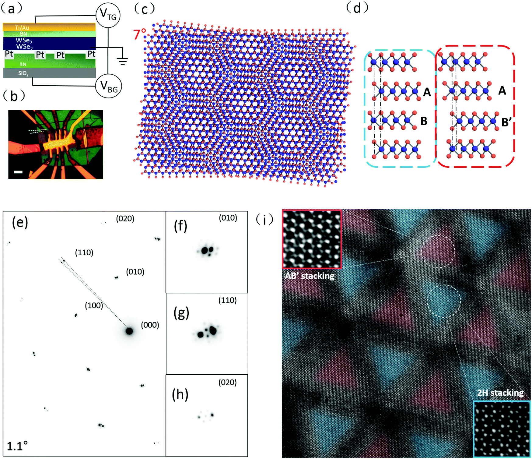 | ||
| Fig. 1 Device structure, stacking model and atomic-scale reconstruction in twist double bilayer WSe2. (a) and (b) Schematic and optical images of the encapsulated twisted double-bilayer WSe2. The scale bar is 6 μm. (c) A schematic moiré superlattice formed by twisted double-bilayer WSe2 flakes. (d) Atomic model of 2H-stacked (ABAB) and AB′-stacked double-bilayer WSe2 viewed along the 〈100〉 zone axis. (e) Electron diffraction pattern taken from a twisted double-bilayer WSe2 with enlarged views of respective Bragg spots (f)–(h), showing the high-order satellites caused by interface reconstruction. (i) Annular dark field image of the interface-reconstructed region, in which 2H/AB′-stacked domains are marked in blue/red. The zoomed-in images illustrate the 2H and AB′ atomic structures. | ||
As verified by aberration-corrected annular dark-field imaging in STEM, the twisted WSe2 bilayers undergo a structural reconstruction and form alternatingly distributed triangular regions as marked in blue and red in Fig. 1i. This structural reconstruction leads to reshaping of the ideal hexagonal moiré pattern (Fig. 1c) to a triangular pattern (Fig. 1i). A detailed model of such a reconstruction and formation of triangular shapes can be found in ref. 30. For a small twist angle, the area of stacking sequence AB′ at the interface between the bilayer WSe2 (as shown schematically in Fig. 1d) extends to form the triangular shape. These 2H and AB′ domains are separated by the triangular network boundaries (the dark contrast strips of about ∼3 nm in width). The narrow domain boundaries have lattice misfit strain as reflected by the dark image contrast. However, the image contrast inside each blue or red area is uniform, meaning that the lattice misfit strain has been relaxed. The scale of the triangular pattern is consistent with the reciprocal space measurement of the electron diffraction pattern. The atomic-resolution images (the insets in Fig. 1i) reveal that 2H and AB′ stacking orders31 of WSe2 exist in the blue and red regions respectively, further verified that the structural reconstruction from a conventional moiré pattern occurs and produces a well-relaxed stacking structure.
The band structure of WSe2 is layer number dependent. In monolayer and bilayer WSe2,32 the valence band maxima locate at K-valleys. In a few-layer WSe2 with a layer number greater than three, Γ-valley heavy holes23 dominate the carrier transport in the valence band edge. In a four-layer WSe2 device, the electrical conductance measured at cryogenic temperatures (see Fig. 2a) monotonically increases with increasing the gate voltage or carrier concentration. In twisted double-bilayer WSe2 (device D11), however, the conductance normally exhibits a few peaks and dips with increasing the gate voltage (see Fig. 2a for the 4° case), indicating the existence of localization states resulted from the moiré superlattice structures. As an example, Fig. 2c illustrates the measured longitudinal resistance of the sample with a 4° twist angle at different gating configurations. By setting the top gate VTG to −22 V (through a 38 nm h-BN layer shown in Fig. S3, ESI†), the channel resistance measured by a four-lead configuration is about 200 Ohms and the corresponding carrier density is 7.5 × 1012 cm−2. The hole mobility calculated by  Considering
  the field effect transistor mobility has reached 1000 cm2 V−1 s−1, which is slightly lower than the high performance devices of monolayer and bilayer WSe2 reported previously.24,33
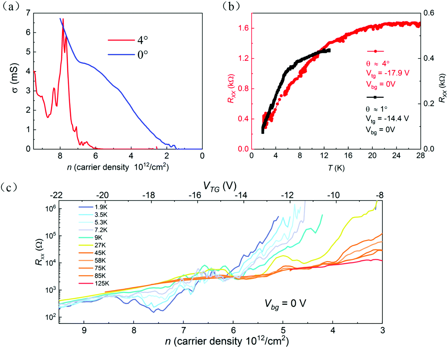 | ||
| Fig. 2 Experimental data of superconductivity obtained from twisted double bilayer WSe2. (a) Conductance of intrinsic four layers WSe2 and twisted double-bilayer WSe2 devices. (b) Quick resistance reduction of the 1° and 4° twisted devices at low temperatures. (c) Longitudinal resistance plotted as a function of the carrier density at different temperatures. The excitation Vds = 1 mV and back gate VBG = 0 V. | ||
For the twisted double-bilayer (totally 4 layers) device, the valence band edges locate at the Γ-valley with a two-fold degeneracy. The nano-ARPES measurement confirmed that the Γ-valley is slightly higher (∼80 meV) than the K-valley (Fig. 3c), which is consistent with that of a previous layer-dependent ARPES study of WSe2.34 Given that, the two peaks shown in the longitudinal resistance at VTG = −15.4 V and −19.8 V in Fig. 2c, could then correspond to the scattering effect of moiré lattice at 6.5 × 1012 cm−2 and at 9 × 1012 cm−2 respectively based on the following estimation. The moiré pattern/superlattice constant35,36 is expressed by 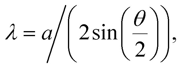 where a is the lattice constant of WSe2. λ is estimated to be 4.7 nm for a 4° twist angle. The full filling of the moiré superlattice (2 holes per moiré unit cell) can be worked out as
 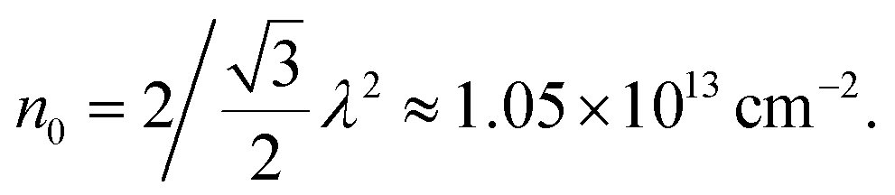 This value is quite close to the carrier concentration calculated according to the quantum capacitance of the WSe2-BN heterostructure. In principle, there are two metallic states adjacent to the correlated half filling insulating states and band insulating states. While here, no insulating sates are observed and we only find metallic states with a few bumps and dips in the four-end resistance. As shown in Fig. 2c, the first one locates at VTG = −14.8 V and displays metallic characteristics since the resistance measured at this gate voltage decreases with decreasing sample temperature from 125 K to 10 K. While, it does not change so much below 10 K. The second one locates between VTG = −16 V to −19.6 V with carrier densities ranging from 5.9 to 8.3 × 1012 cm−2. It has a metallic behavior in the temperature region of 125–11 K. The measured resistance decreases gradually with decreasing sample temperature, which means that phonon scattering dominates in the electron transport behavior. From 11 K to 1.9 K, however, a quick reduction of the resistance (from 1600 to 200 Ohms) occurs as shown in Fig. 2b. Such a quick reduction of the channel resistance is possibly attributed to the formation of superconducting states at the interface of twisted double-bilayer WSe2. Because of the impurity-dominated scattering in WSe2, the intrinsic resistance of a few-layer WSe2 device normally remains almost as a constant value at very low temperatures,37 and has no contribution to the observed quick reduction of the channel resistance.
 | ||
| Fig. 3 ARPES data obtained from device A3 (twist angle 3.5°). (a) The optical image of the device. The twisted double bilayer area is marked by the blue circle. (b) Scanning photoemission microscopy image of the device. The intensity of the map represents the counts of photoelectron near EF (c) electronic band dispersion along Γ–K points to show the four-band Γ-valley characteristics of the twisted double bilayer WSe2 area. The ARPES measurement was performed at the red spot marked in (b). | ||
The flat bands formed at the edges of the valence band in WSe2 moiré superlattice have been predicted theoretically.17,18,21 The bandwidth is comparable to that of twisted graphene at the ‘magic’ angle. In these flat bands, the kinetic energy is quenched (Ek ∼ 10 meV) which is in the same order as the on-site Coulomb interaction 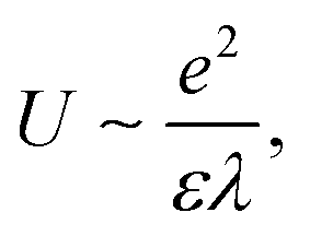 where ε = 4 is the dielectric constant of h-BN. For λ = 4.7 nm, the Coulomb interaction is about dozens of meV. This could lead to the superconducting states at the interface of twisted double-bilayer WSe2. By fixing the carrier density at 7.5 × 1012 cm−2, we observe that the longitudinal resistance decreases quickly when sample temperature is below 18 K (Fig. 2b). This transition temperature is much higher than the highest onset transition temperature of twisted graphene. At 6 K, the channel resistance drops to 800 Ω, about half of the normal metallic state resistance.
To investigate the electronic band structure of the twisted double bilayer WSe2, we have performed state-of-the-art nano-ARPES measurement on the devices without top gates. Fig. 3a presents the optical image of the devices used in the ARPES measurement. The size of the twisted area (marked by the blue circle) is around 10 × 20 μm2, which is sufficiently large compared with the ARPES spot size. Fig. 3b is the scanning photoemission microscopy image of one device, in which the intensity represents the counts of photoelectrons near the Fermi level. Thus, the gold pad and the graphite gate area have a relatively higher intensity than the WSe2 area. By comparing Fig. 3a and b, the twisted area can be located for the ARPES measurement. The electronic band dispersion along Γ–K points is shown in Fig. 3c. At the Γ point, we can identify four bands near the valence band top, which indicates strong interlayer coupling in the twisted double bilayer system. As the number of the bands at Γ-valley in WSe2 is determined by the layer number, the observation of four-band Γ-valley suggests that the electronic structure of the twisted double bilayer system is close to the intrinsic 4-layer system. This means the electronic states in top and bottom bilayers have been unified into an integrated system by the interlayer interaction. Furthermore, we find that the Γ-valley is slightly higher (∼80 meV) than the K-valley, which implies that the Γ valley have more contribution to the electrical properties in the p-doped region. This discovery distinguishes this sample system from twisted graphene or twisted bilayer WSe2 whose valence band maxima locate at the boundaries of the Brillouin zone.
The transport characteristics of the twisted WSe2 show a similar behavior of superconductivity in twisted graphene structures. Our finding suggests that the interaction effects induced by twisting bilayer WSe2 are substantial. Due to the structural inhomogeneity in our twisted layer WSe2, the resistance cannot reduce further at cryogenic temperatures. As observed by atomic-resolution electron microscopy, the twist angle often slightly changes from area to area, resulting in micrometer-sized domains in the sample. Because our device size is about a few micrometers, the electrodes for transport measurement may cross more than one domain or more than one superconducting domain if superconducting state exists in each domain or in some domains.38 The reason why twisted WSe2 have a high-density of domains is unclear. This could be introduced by fabrication or originated from the intrinsic structure properties of WSe2 since in each layer of WSe2 there are three atomic layers of tungsten and selenium atoms. The atomic bonds in WSe2 are weaker than the sp2 bonds in graphene. This may result in slight deviation of the twist angle by locally non-uniform strains at the interface.
A small twist angle leads to the formation of a large moiré superlattice cell. For E7 device (1° twist angle and λ ≈ 19 nm), fully filling the moiré superlattice requires 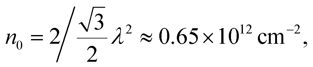 an order of magnitude smaller than that of the 4° twist sample. Similarly, by changing the top-gate voltage, we observe multiple superconducting-like states in the 1° twist device (Fig. 4a), which could be resulted from the high-order flat bands. The thickness of the h-BN dielectric layer in this device is about 44 nm (shown in Fig. S6, ESI†). The separation between the first and second superconducting-like domes is V ≈ 1 V, corresponding to a carrier density of 0.66 × 1012 cm−2, which is very close to the full filling state of the moiré superlattice unit cell shown in Fig. 1i. In Fig. 2b, we find that the resistance remains nearly a constant value above 5 K, and a quick resistance drop occurs below 5 K.
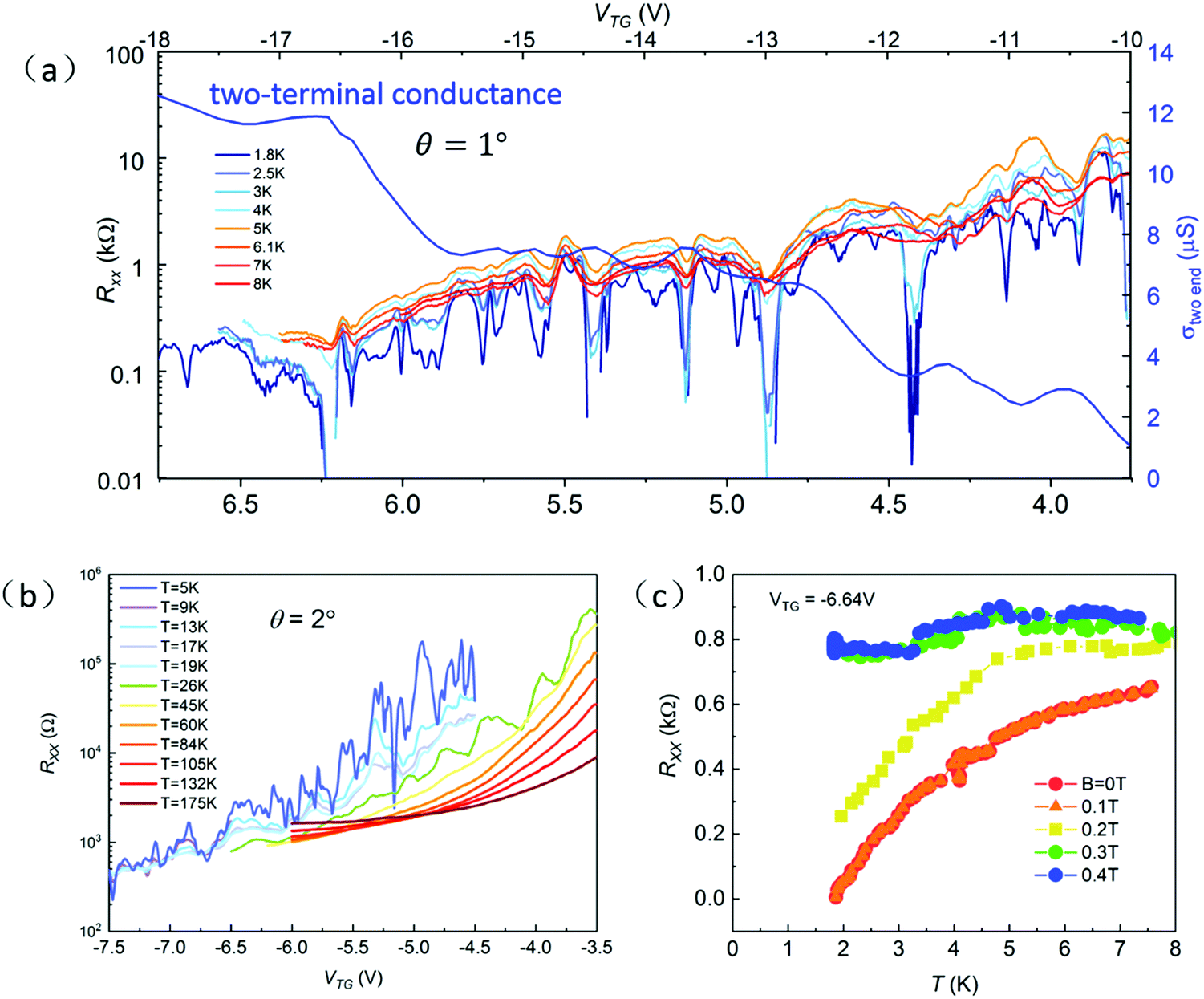 | ||
| Fig. 4 Transport characteristics in 1°, 2° twisted double bilayer WSe2. (a) The resistance (four terminal measurement) of Sample E7 with a twisting angle of about 1° at various temperatures (1.9 K to 8 K). The right blue line is the two terminal conductance of the same sample. (b) The resistance (four terminal measurement) of Sample F2 with a twisting angle of about 2° at various temperatures (1.9 K to 8 K). (c) The longitude resistance of Sample F2 at VTG = −6.64 V, plotted as a function of temperature with various perpendicular magnetic fields. | ||
We suggest that the multiple superconducting-like domes shown in Fig. 4a are attributed to the high-order flat bands. Because of structural inhomogeneity in the twisted structures, the domes do not occur periodically. Fig. 4b illustrates the longitudinal resistance of another small angle of 2° twist sample. Multiple bumps and dips are clearly visible. In addition to the similar thermal effects on the superconductor states, we observe that a perpendicular magnetic field can change the superconducting-like states to normal metallic states. In Fig. 4c, the longitude resistance does not change when the magnetic field is above 0.3 T, which means the system become a normal metallic state if the magnetic field is higher than 0.3 T.
Fig. 5a shows the transport characteristics of device F2 (twist angle 2 ± 0.5°), in which the longitude resistance is measured by setting the top gate at −6.65 V and −6.92 V. The carrier density is estimated to be around n0 = 6 × 1012 cm−2 and 7 × 1012 cm−2. Considering the full filling states of n0 = 2.6 × 1012 cm−2 for a 2° twist angle, we attribute that the electrons possibly reside on the high order flat bands18,39 of the Γ-valley in this sample. For VTG = −6.65 V, the resistance keeps a constant value from 30 K to 9 K and quickly drops down from 9 K to 2 K. It reaches a zero resistance with an uncertainty of ±10 Ohms. At VTG = −6.92 V, the resistance keeps a constant value from 20 K to 10 K and quickly drops down from 10 K to 2 K to reach a zero resistance at about 3 K. Fig. 5b demonstrates a typical non-linear I–V curve observed at VTG = −6.64 V. At 1.8 K, the critical current for hosting the zero resistance is about 25 nA. According to the experimental data collected from the samples with different twist angles, we confirm that enhanced interlayer interactions which are similar to that in twisted graphene are generated. Because of the structural inhomogeneity in the twisted WSe2 devices, precisely measuring the superconductivity parameters, for example, the critical current density undergoes difficulties. This is because the induced electric field via Vds across the inhomogeneous domains and domain boundaries cannot be well defined. On the other hand, the van der Waals interface structure in the twist devices may be in an unstable state since annealing of the devices very often causes the twist angle changes. However, our experimental results qualitatively demonstrate the superconductivity signatures in twisted WSe2 structures.
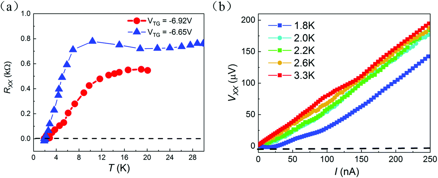 | ||
| Fig. 5 Superconductivity characteristics in 2° twisted double bilayer WSe2. (a) Longitudinal resistance measured by the four-terminal configuration of the 2° twist device. (b) The I–V curves measured from device F2 at different temperatures. The VTG is set at −6.65 V. | ||
In conclusion, we successfully fabricated double-bilayer twisted WSe2 devices with well-controlled twist angles. Reconstructed moiré superlattices are observed in the samples with 1° twist angle. WSe2 moiré lattices can host full filling carrier densities ranging from 0.65 × 1012 cm−2 to 1.05 × 1013 cm−2. Enhanced interlayer interactions are observed when the twist angle decreases to a few degrees as reflected by the high-order satellites in the electron diffraction patterns taken from the reconstructed domains from a conventional moiré superlattice. We demonstrate transport characteristics with superconductivity signatures measured at cryogenic temperatures which are modulated by the reconstructed moiré superlattices and inhomogeneous domains. With strong intrinsic electron–electron interaction effects and large effective masses, atomically thin twisted WSe2 provides a new platform for studying the correlated phenomena of 2D electrons.
Author contributions
LHA fabricated twist double bilayer WSe2 devices and TEM samples. LHA, JXZL, ZFW, HMZ performed and analyzed the transport measurements under supervision of NW. LHA, ZFW, HMZ and NW analyze the quantum transport data. XBC took and analyzed the HRTEM image for the twist WSe2. DP performed the ARPES experiment with the assistance of CC and MW. Other authors provided technical assistance on sample preparations and measurements and discussed on the paper. LHA and NW wrote the paper with input from all authors.Conflicts of interest
There are no conflicts to declare.Acknowledgements
We thank Prof. Xi Dai, Prof. K. T. Law, Prof. Nian Lin, Dr Jianpeng Liu and Dr Wenyu He, Dr Tong Zhou, Dr En Li, from HKUST for fruitful discussions. This work is supported by the Research Grants Council of Hong Kong (Project No. 16300717 and C7036-17W) and EPSRC (grant no. EP/M020517/1). We acknowledge the technical support from the Super-resolution Electron Microscopy facility and Raith-HKUST Nanotechnology Laboratory for the electron-beam lithography facility at MCPF, and the support from Beamline I05, Diamond Light Source (proposal no. SI24366). Ding Pei thanks the support from Chinese Scholarship Council.References
- Y. Cao, V. Fatemi, S. Fang, K. Watanabe, T. Taniguchi, E. Kaxiras and P. Jarillo-Herrero, Nature, 2018, 556, 43–50 CrossRef CAS PubMed.
- Y. Cao, V. Fatemi, A. Demir, S. Fang, S. L. Tomarken, J. Y. Luo, J. D. Sanchez-Yamagishi, K. Watanabe, T. Taniguchi, E. Kaxiras, R. C. Ashoori and P. Jarillo-Herrero, Nature, 2018, 556, 80–84 CrossRef CAS PubMed.
- A. L. Sharpe, E. J. Fox, A. W. Barnard, J. Finney, K. Watanabe, T. Taniguchi, M. A. Kastner and D. Goldhaber-Gordon, Science, 2019, 365, 605–608 CrossRef CAS PubMed.
- A. H. MacDonald, Physics, 2019, 12, 12 CrossRef.
- X. Lu, P. Stepanov, W. Yang, M. Xie, M. A. Aamir, I. Das, C. Urgell, K. Watanabe, T. Taniguchi and G. Zhang, 2019, arXiv preprint arXiv:1903.06513.
- M. Serlin, C. Tschirhart, H. Polshyn, Y. Zhang, J. Zhu, K. Watanabe, T. Taniguchi, L. Balents and A. Young, Science, 2019, 8 Search PubMed.
- W.-Y. He, D. Goldhaber-Gordon and K. Law, 2019, arXiv preprint arXiv:1908.11718.
- X. Liu, Z. Hao, E. Khalaf, J. Y. Lee, K. Watanabe, T. Taniguchi, A. Vishwanath and P. Kim, 2019, arXiv preprint arXiv:1903.08130.
- C. Shen, N. Li, S. Wang, Y. Zhao, J. Tang, J. Liu, J. Tian, Y. Chu, K. Watanabe and T. Taniguchi, 2019, arXiv preprint arXiv:1903.06952.
- A. Kerelsky, C. Rubio-Verdú, L. Xian, D. M. Kennes, D. Halbertal, N. Finney, L. Song, S. Turkel, L. Wang and K. Watanabe, 2019, arXiv preprint arXiv:1911.00007.
- G. Chen, L. Jiang, S. Wu, B. Lyu, H. Li, B. L. Chittari, K. Watanabe, T. Taniguchi, Z. Shi and J. Jung, Nat. Phys., 2019, 15, 237 Search PubMed.
- P. Lucignano, D. Alfè, V. Cataudella, D. Ninno and G. Cantele, Phys. Rev. B, 2019, 99, 195419 CrossRef CAS.
- N. F. Yuan and L. Fu, Phys. Rev. B, 2018, 98, 045103 CrossRef CAS.
- J. Liu, J. Liu and X. Dai, Phys. Rev. B, 2019, 99, 155415 CrossRef CAS.
- K. L. Seyler, P. Rivera, H. Yu, N. P. Wilson, E. L. Ray, D. G. Mandrus, J. Yan, W. Yao and X. Xu, Nature, 2019, 567, 66 CrossRef CAS PubMed.
- C. Jin, E. C. Regan, A. Yan, M. I. B. Utama, D. Wang, S. Zhao, Y. Qin, S. Yang, Z. Zheng and S. Shi, Nature, 2019, 567, 76 CrossRef CAS PubMed.
- M. H. Naik and M. Jain, Phys. Rev. Lett., 2018, 121, 266401 CrossRef CAS PubMed.
- F. Wu, T. Lovorn, E. Tutuc, I. Martin and A. MacDonald, Phys. Rev. Lett., 2019, 122, 086402 CrossRef CAS PubMed.
- M. Fleischmann, R. Gupta, S. Sharma and S. Shallcross, arXiv preprint arXiv:1901.04679, 2019.
- L. Wang, E.-M. Shih, A. Ghiotto, L. Xian, D. A. Rhodes, C. Tan, M. Claassen, D. M. Kennes, Y. Bai and B. Kim, arXiv preprint arXiv:1910.12147, 2019.
- F. Wu, T. Lovorn, E. Tutuc and A. H. MacDonald, Phys. Rev. Lett., 2018, 121, 026402 CrossRef CAS PubMed.
- F. Conte, D. Ninno and G. Cantele, Phys. Rev. B, 2019, 99, 155429 CrossRef CAS.
- S. Xu, J. Shen, G. Long, Z. Wu, Z. Q. Bao, C. C. Liu, X. Xiao, T. Han, J. Lin, Y. Wu, H. Lu, J. Hou, L. An, Y. Wang, Y. Cai, K. M. Ho, Y. He, R. Lortz, F. Zhang and N. Wang, Phys. Rev. Lett., 2017, 118, 067702 CrossRef PubMed.
- H. C. P. Movva, B. Fallahazad, K. Kim, S. Larentis, T. Taniguchi, K. Watanabe, S. K. Banerjee and E. Tutuc, Phys. Rev. Lett., 2017, 118, 247701 CrossRef PubMed.
- J. Lin, T. Han, B. A. Piot, Z. Wu, S. Xu, G. Long, L. An, P. Cheung, P. P. Zheng, P. Plochocka, X. Dai, D. K. Maude, F. Zhang and N. Wang, Nano Lett., 2019, 19, 1736–1742 CrossRef CAS PubMed.
- Y. Wang, C. Sun, X. Yan, F. Xiu, L. Wang, S. C. Smith, K. L. Wang, G. Q. Lu and J. Zou, J. Am. Chem. Soc., 2011, 133, 695–697 CrossRef CAS PubMed.
- S. Xu, Z. Wu, H. Lu, Y. Han, G. Long, X. Chen, T. Han, W. Ye, Y. Wu, J. Lin, J. Shen, Y. Cai, Y. He, F. Zhang, R. Lortz, C. Cheng and N. Wang, 2D Mater., 2016, 3, 021007 CrossRef.
- Z. Wu, S. Xu, H. Lu, A. Khamoshi, G.-B. Liu, T. Han, Y. Wu, J. Lin, G. Long and Y. He, Nat. Commun., 2016, 7, 12955 CrossRef CAS PubMed.
- H. C. Movva, A. Rai, S. Kang, K. Kim, B. Fallahazad, T. Taniguchi, K. Watanabe, E. Tutuc and S. K. Banerjee, ACS Nano, 2015, 9, 10402–10410 CrossRef CAS PubMed.
- H. Yoo, R. Engelke, S. Carr, S. Fang, K. Zhang, P. Cazeaux, S. H. Sung, R. Hovden, A. W. Tsen, T. Taniguchi, K. Watanabe, G. C. Yi, M. Kim, M. Luskin, E. B. Tadmor, E. Kaxiras and P. Kim, Nat. Mater., 2019, 18, 448–453 CrossRef CAS PubMed.
- S. Zhu and H. T. Johnson, Nanoscale, 2018, 10, 20689–20701 RSC.
- H. C. Movva, B. Fallahazad, K. Kim, S. Larentis, T. Taniguchi, K. Watanabe, S. K. Banerjee and E. Tutuc, Phys. Rev. Lett., 2017, 118, 247701 CrossRef PubMed.
- B. Fallahazad, H. C. Movva, K. Kim, S. Larentis, T. Taniguchi, K. Watanabe, S. K. Banerjee and E. Tutuc, Phys. Rev. Lett., 2016, 116, 086601 CrossRef PubMed.
- Y. Zhang, M. M. Ugeda, C. Jin, S.-F. Shi, A. J. Bradley, A. Martín-Recio, H. Ryu, J. Kim, S. Tang and Y. Kim, Nano Lett., 2016, 16, 2485–2491 CrossRef CAS PubMed.
- R. Bistritzer and A. H. MacDonald, Proc. Natl. Acad. Sci. U. S. A., 2011, 108, 12233–12237 CrossRef CAS PubMed.
- K. Kim, A. DaSilva, S. Huang, B. Fallahazad, S. Larentis, T. Taniguchi, K. Watanabe, B. J. LeRoy, A. H. MacDonald and E. Tutuc, Proc. Natl. Acad. Sci. U. S. A., 2017, 114, 3364–3369 CrossRef CAS PubMed.
- S. Xu, Z. Wu, H. Lu, Y. Han, G. Long, X. Chen, T. Han, W. Ye, Y. Wu and J. Lin, 2D Mater., 2016, 3, 021007 CrossRef.
- T. Han, J. Shen, N. F. Yuan, J. Lin, Z. Wu, Y. Wu, S. Xu, L. An, G. Long and Y. Wang, Phys. Rev. B, 2018, 97, 060505 CrossRef CAS.
- M. H. Naik and M. Jain, Phys. Rev. Lett., 2018, 121, 266401 CrossRef CAS PubMed.
Footnotes |
| † Electronic supplementary information (ESI) available. See DOI: 10.1039/d0nh00248h |
| ‡ These authors contributed equally to this work. |
| This journal is © The Royal Society of Chemistry 2020 |