
Controlled growth of large-scale uniform 1T′ MoTe2 crystals with tunable thickness and their photodetector applications†
Xiaojian
Wang‡
a,
Jing
Shang‡
 bc,
Meijie
Zhu‡
a,
Xi
Zhou
d,
Rui
Hao
d,
Lina
Sun
d,
Hua
Xu
e,
Jianbang
Zheng
*a,
Xingfeng
Lei
d,
Chun
Li
c,
Liangzhi
Kou
*b and
Qingliang
Feng
*ad
bc,
Meijie
Zhu‡
a,
Xi
Zhou
d,
Rui
Hao
d,
Lina
Sun
d,
Hua
Xu
e,
Jianbang
Zheng
*a,
Xingfeng
Lei
d,
Chun
Li
c,
Liangzhi
Kou
*b and
Qingliang
Feng
*ad
aMOE Key Laboratory of Material Physics and Chemistry under Extraordinary Conditions, School of Science, Northwestern Polytechnical University, Xi’an 710072, P. R. China. E-mail: zhengjianbang@nwpu.edu.cn
bSchool of Mechanical, Medical and Process Engineering, Queensland University of Technology, Brisbane, QLD 4001, Australia. E-mail: liangzhi.kou@qut.edu.au
cSchool of Mechanics, Civil Engineering and Architecture, Northwestern Polytechnical University, Xi’an 710072, China
dKey Laboratory of Special Functional and Smart Polymer Materials of Ministry of Industry and Information Technology, School of Chemistry and Chemical Engineering, Northwestern Polytechnical University, Xi’an 710072, P. R. China. E-mail: fengql@nwpu.edu.cn
eSchool of Materials Science and Engineering, Shaanxi Normal University, Xi’an 710119, P. R. China
First published on 20th March 2020
Abstract
The monoclinic-phase 1T′ MoTe2 crystal exhibits inversion symmetry as an anisotropic semi-metal, dictating its interesting quantum transport phenomenon and other novel physical properties. However, large-scale controllable growth of uniform MoTe2 crystals still remains a great challenge, hindering its further fundamental research and applications for novel devices. Herein, we report a modified growth method for synthesizing few-layer 1T′ MoTe2 crystals with large-scale uniformity with the assistance of molecular sieves. The theoretical simulations demonstrated that due to the temperature-dependent formation energies of different edges, the edge of (010) orientation shows a higher thermodynamic stability than that of (100) orientation, and results in the anisotropic growth behavior of 1T′ MoTe2 crystals while the temperature changes. The photoresponse of tri-layer 1T′ MoTe2-based devices shows a broad-spectrum response from 532 nm to 1550 nm. The photo-response time of 1T′ MoTe2 crystals demonstrates that it supposes to be the synergistic mechanism of photo-conductive and photo-radiation effects. Our findings not only provide a method for the controllable growth of anisotropic two-dimensional materials at a wafer scale, but also explore a broad-spectrum photodetector with the MoTe2-based device.
New conceptsDue to the spatial symmetry of 1T′ MoTe2 crystal, it has shown anisotropic optical, electronic and chemical properties, endowing it with great advantages for the potential application in polarized broad-spectrum detectors and nonlinear optical devices. However, the low-temperature nucleation of precursors and anisotropic crystal structures makes it difficult to control the morphology and layer-thickness during the synthesis process of 1T′ MoTe2 crystals. The novelty of this work is to demonstrate a physical layer of molecular sieves to restore and sustain the release of Mo precursors to obtain few-layer 1T′ MoTe2 crystals with large-scale uniformity. The temperature-dependent formation energies of (010) orientation (Mo chains) edges are lower than (100) orientation edges by density-functional ab initio molecular dynamics (AIMD) simulations, which is the specific reason for the controllable growth of the morphology and thickness of 1T′ MoTe2 crystals. Due to the semi-metal phase of few-layer 1T′ MoTe2, it has shown a broad-spectrum response from 532 to 1550 nm with a synergistic effect of photo-conductive and photo-radiation mechanisms. This work creates a universal method for the controllable synthesis of two-dimensional materials at wafer scale with uniform morphology, and explores a broad-spectrum photo-detector with few-layer MoTe2 crystals. |
Two-dimensional transition metal dichalcogenides (TMDs) have attracted considerable attention in recent years owing to their unique electronic and optical properties, high carrier mobility and novel physical properties.1–5 As a member of the TMD family, MoTe2 possesses not only a stable semiconducting 2H phase but also a metastable semi-metallic 1T′ phase. Due to the distorted octahedral structure, anisotropic semi-metal 1T′ MoTe2 crystals show several interesting properties, such as superconductivity, ferroelectricity, magnetoresistance, large-gap quantum spin Hall insulators and Weyl semimetals, all of which make them greatly attractive for high-efficiency thermoelectric devices, novel switching devices and topological field effect transistors.6–13
Controllable synthesis of large-area and high-quality 1T′ MoTe2 with a single crystal is a key step to its further fundamental aspects and applications in new concept devices.14,15 To date, some methods such as the telluridation of Mo films, the mixed precursor of metal salts, the iodine vapor transport assistance, the NaCl assistance and so on have been reported to successfully synthesize 2D MoTe2 crystals.16–21 However, due to the uncontrollable vapor process for the concentration of precursors and the advanced nucleation at low temperatures, the layer thickness, morphology and nucleation uniformity in large scale were not well controlled yet.22 Understanding the growth mechanism is the key issue to resolve this challenge, which also encourages us to develop a new method for the growth of large-scale uniform single-crystal MoTe2.
Herein, we report a modified growth method to obtain few-layer 1T′ MoTe2 crystals with uniform morphology and layer thickness in large scales finally. Due to the controllable release of Mo precursors using a molecular sieve, we realize the homogeneous nucleation in an ultra large scale on the SiO2/Si substrate. The domain size of single-crystal 1T′ MoTe2 is almost up to ∼100 μm. Combining ab initio molecular dynamics and growth thermodynamics analysis, the results indicate that the edge formation energy of 1T′ MoTe2 is strongly dependent on the temperature, and led to the (010) orientation that is faster than the (100) orientation with an anisotropic growth mode, and obtained a ribbon shape morphology finally. Our findings explain not only the anisotropic growth behavior of two-dimensional materials in detail but also the application of 1T′ MoTe2 for its further fundamental investigation in condensed matter physics and new concept devices.
The schematic of the controllable synthesis of large-scale uniform single-crystal 1T′ MoTe2 is shown in Fig. 1a; the Te powder and MoO3 powder are put in the ceramic boat at the upstream and center of the furnace, respectively. What is more, some molecular sieves are added, which fully covered the MoO3 powder; they play multiple roles during this growth process. The gaseous molecules of Mo precursors (MoOxCly, and MoOx) diffused into the porous structure of molecular sieves when the growth temperature increased. First, it can delay the Mo precursor transfer to the surface of the substrate as a physical barrier before the temperature reaches the optimized growth temperature, which is very important for the clean and uniform growth. What is more, it can also work as the micro container to restore, sustain the release of the Mo precursor during the heating and growth process, and assist to obtain single-crystal 1T′ MoTe2 with uniform morphology and layer thickness in large scales finally. NaCl powder serves as an assisting agent to increase the vapor pressure of the Mo precursor at low temperatures, that is MoO3 will change to low-melting point MoOxCly and to vapor easily. The OM images of the as-grown 1T′ MoTe2 crystals, which are synthesized with and without molecular sieve assistance, respectively, are shown in Fig. S1 (ESI†). The left one shows the uncontrollable growth behavior on the substrate (Fig. S1b, ESI†). Most of the area at the center of the substrate are thick layers, as shown in Fig. S1c (ESI†), and the thinner layers also grow at the edge region of the substrate, as shown in Fig. S1d (ESI†). The right one shows the uniform growth behavior on the substrate (Fig. S1e, ESI†) by the modified growth method, and the as-obtained 1T′ MoTe2 crystals with uniform morphology and layer thickness in large scales (Fig. S1e–g, ESI†). The atomic mode of 1T′ MoTe2 crystal structures is shown in Fig. 1b, revealing an obvious anisotropic structure; the Mo chain direction is the (010) orientation and the other one is the (100) orientation.
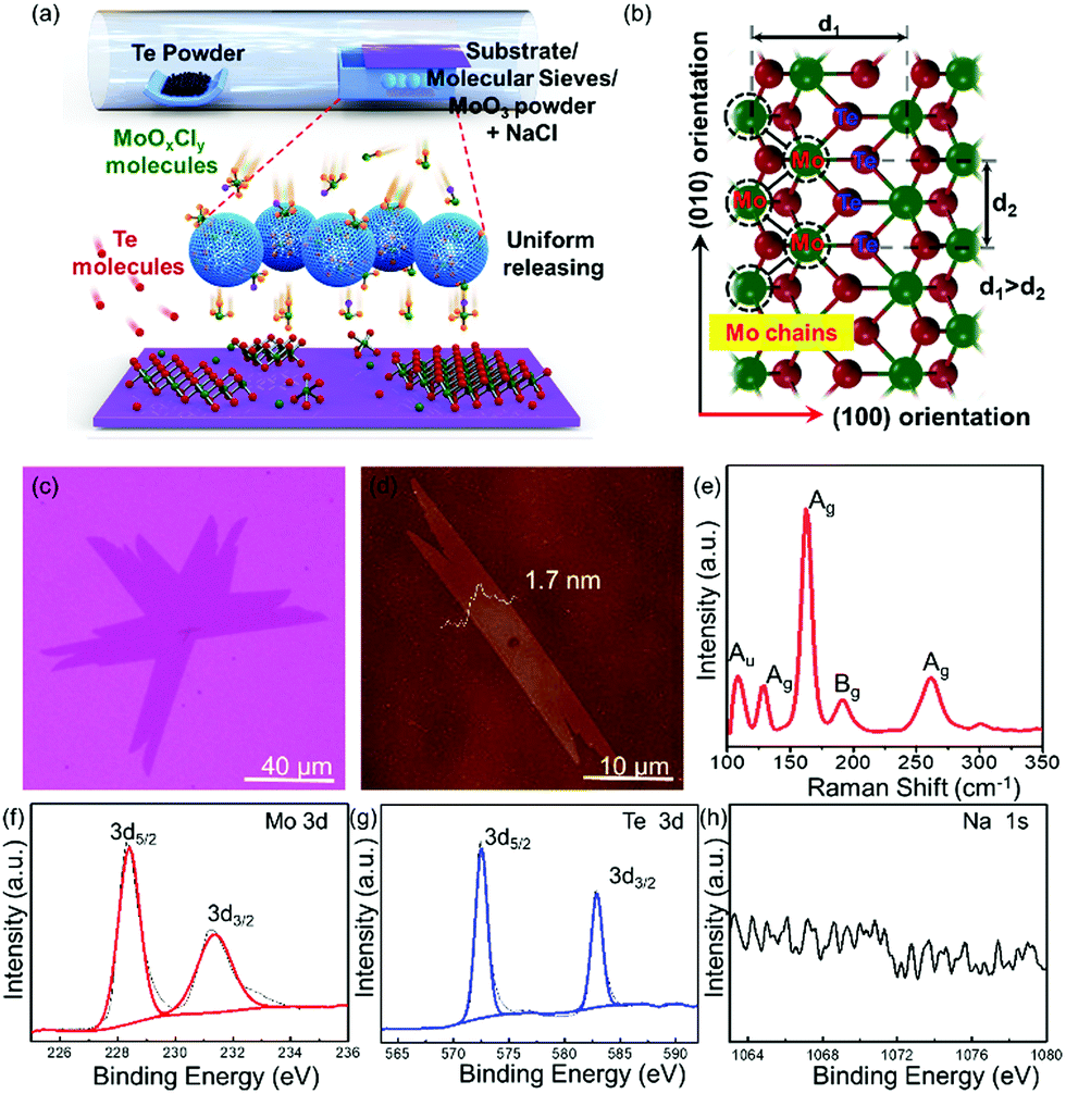 | ||
| Fig. 1 Modified CVD growth of 1T′ MoTe2 crystals: (a) schematic of synthesized 1T′ MoTe2 crystals with uniform morphology in large scales. (b) Atomic structure of 1T′ MoTe2 crystals in two orientations. (c) Optical images of the as-synthesized bilayer 1T′ MoTe2 crystals with the growth temperature at 750 °C. (d) AFM images of the ribbon shape of 1T′ MoTe2 with a thickness of 1.7 nm. (e) Typical Raman spectra of bilayer 1T′ MoTe2 crystals. (f–h) High-resolution XPS spectra of Mo elements, Te elements and Na elements of 1T′ MoTe2 crystals on the SiO2/Si substrate. | ||
In Fig. 1c, the OM image of 1T′ MoTe2 single crystals show a ribbon-shape with a domain size up to 100 μm. Atomic force microscopic (AFM) images of the as-grown 1T′ MoTe2 crystals are shown in Fig. 1d with a height of 1.7 nm, which demonstrated the three-layered structure of 1T′ MoTe2. Fig. 1e is the typical Raman spectra of the as-obtained 1T′ MoTe2 crystals; the peaks at around 108.36 cm−1, 128.58 cm−1, 163.02 cm−1, 191.42 cm−1 and 261.38 cm−1 are corresponding to the Raman mode of Au, Ag, Ag, Bg, and Ag of 1T′ MoTe2, respectively.23,24 X-ray photoelectron spectroscopy (XPS) was performed to confirm the chemical composition of the as-grown 1T′ MoTe2 films on 280 nm SiO2/Si. The high-resolution spectra of Mo elements, Te elements and Na elements, and the full spectra of 1T′ MoTe2 films are shown in Fig. 1f–h and Fig. S2 (ESI†). In Fig. 1f, there is only one couple of peaks for Mo elements, which are located at 228.3 eV and 231.2 eV, respectively. In Fig. 1g, one couple of peaks of Te elements are located at 572.4 eV and 582.8 eV, respectively,15–21 while there were no obvious peaks of Na 1s in Fig. 1h, which means that the Na elements are not residues in the substrate. In addition, there were several elements such as the Mo, Te, Si, C and O that appeared in Fig. S2 (ESI†), which were contributed from the substrate and 1T′ MoTe2 films. The chemical ratio between the Mo elements and Te elements is around 1![[thin space (1/6-em)]](https://www.rsc.org/images/entities/char_2009.gif) :2.02, which demonstrated that the as-synthesized 1T′ MoTe2 crystal shows low defects and a perfect crystal structure.
:2.02, which demonstrated that the as-synthesized 1T′ MoTe2 crystal shows low defects and a perfect crystal structure.
High-resolution transmission electron microscopy (HRTEM) and selected-area electron diffraction (SAED) are both used to investigate the crystalline structure of the tri-layer 1T′ MoTe2 crystal. Fig. 2a shows the normal TEM image of tri-layer 1T′ MoTe2 crystals, and the top right corner is the OM images of ribbon-shaped samples. The HRTEM images of 1T′ MoTe2 crystals are shown in Fig. 2b and c, respectively. The HRTEM image in Fig. 2b shows the (100) lines with a spacing of 0.612 nm and the (010) lines with a spacing of 0.344 nm. Fig. 2c also shows the zoom-in image of HRTEM for 1T′ MoTe2.20 The SAED pattern (Fig. 2d) shows only one set of monoclinic spots, demonstrating the fine structure of as-synthesized 1T′ MoTe2 as a single crystal. Fig. 2e shows the SAED patterns for the randomly selected area of the as-synthesized ribbon-shape 1T′ MoTe2 crystals, all of which show the same pattern parameters with only one set of monoclinic spots. The HAADF of 1T′ MoTe2, and the EDX mapping of Mo elements and Te elements of single-crystal 1T′ MoTe2 are shown in Fig. 2f–h; both the Mo elements and Te elements are both randomly distributed in the selected area, demonstrating the uniform composition of the as-obtained single-crystal 1T′ MoTe2.
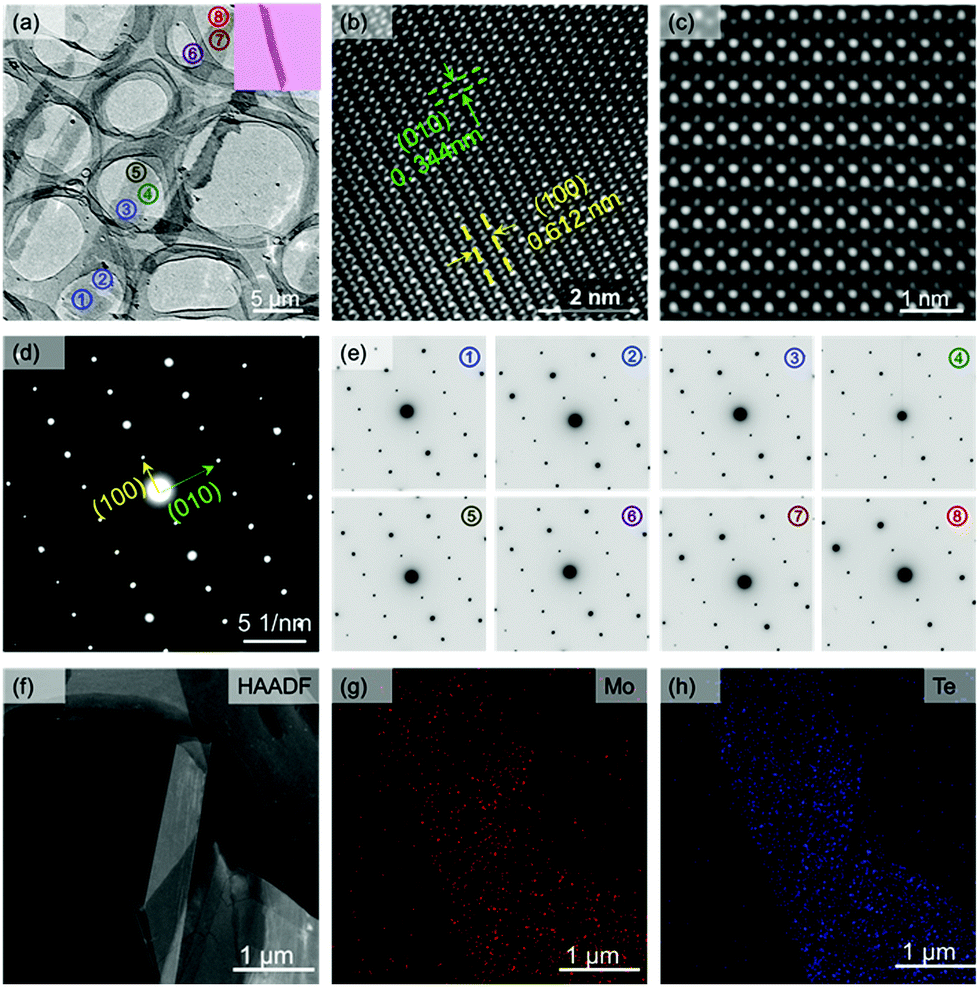 | ||
| Fig. 2 Characterization of the crystalline structure of the as-grown 1T′ MoTe2 crystals. (a) Normal TEM image of 1T′ MoTe2 crystals with the growth temperature at 800 °C. (b and c) HRTEM images of the as-synthesized 1T′ MoTe2 crystal. (d and e) SAED patterns of 1T′ MoTe2 in large area and 8 randomly selected positions, respectively. (f–h) HAADF-STEM image, and EDS mapping of Te and Mo elements. | ||
Different layers of 1T′ MoTe2 films on the 270 nm SiO2/Si substrate are shown in Fig. S3a (ESI†), including monolayer (1L), bilayer (2L), tri-layer (3L), as well as few-layer (FL) structures. The normal Raman spectra of monolayer, bilayer, tri-layer and few-layer structures of 1T′ MoTe2 are shown in Fig. S3b (ESI†). Both the peak position and peak intensity show irregular evolution with the increase in layer thickness. Hence, different from other TMDs, the Raman spectra cannot be used to determine the layer number of anisotropic 1T′ MoTe2. The contrast of OM images for different layers is extracted with red (R), green (G) and blue (B) values in Fig. S3c (ESI†).25 What is more, a selected sample of 1T′ MoTe2 with a special morphology is shown in Fig. S3d (ESI†). The Raman spectra of different positions marked in Fig. S3e (ESI†) show different Raman peaks and irregular peak intensity evolution, while the G values of the optical contrast at three marked positions are nearly the same (Fig. S3f, ESI†). The 1T′ MoTe2 films with different layers have been transferred to 300 nm SiO2/Si, and the G value, B value and R value also show a similar evolution. Finally, we have developed a convenient method to confirm the thickness of 1T′ MoTe2 films by the G value of the optical contrast.
The thermodynamic stability of 1T′ MoTe2 crystals is investigated by the aspect of growth temperature. With the increase in growth temperatures from 650 °C to 800 °C, the morphology of the sample tends to be regular and the thickness increases gradually. When the temperature is 650 °C, the as-grown MoTe2 crystals show an irregular dendritic shape (Fig. 3a), and the optical contrast of the G channel was about 0.263 (Fig. 3e), which corresponds to the 1L thickness. As the temperature increased to 700 °C, almost all of the samples are hexagon-shaped (Fig. 3b), and the central value of the G channel optical contrast increased to 0.337 (Fig. 3f), matching to a thickness of 2L. As displayed in Fig. 3c and g, the samples prepared at 750 °C show a lower overall branching (≤6) and the edges tend to be regular, while the thickness of MoTe2 is not changed. Continuous heating up to 800 °C transformed the samples from polycrystalline structures to single-crystal structures, which present a ribbon-shaped morphology with a corresponding G-channel optical contrast of 0.577 (3L), as shown in Fig. 3d and h. In Fig. S4 (ESI†), the thicknesses of the related samples of MoTe2 are also confirmed by AFM to support the involution of the G values of different layers. Similar to the controllable growth of vertical heterojunctions of two-dimensional transition metal dichalcogenides, we suppose the thickness controlling mechanism with different temperatures should also contribute to the diffusion barrier energy of the interlayer of 1T′ MoTe2. As a result, higher temperatures induce more layers of 1T′ MoTe2.
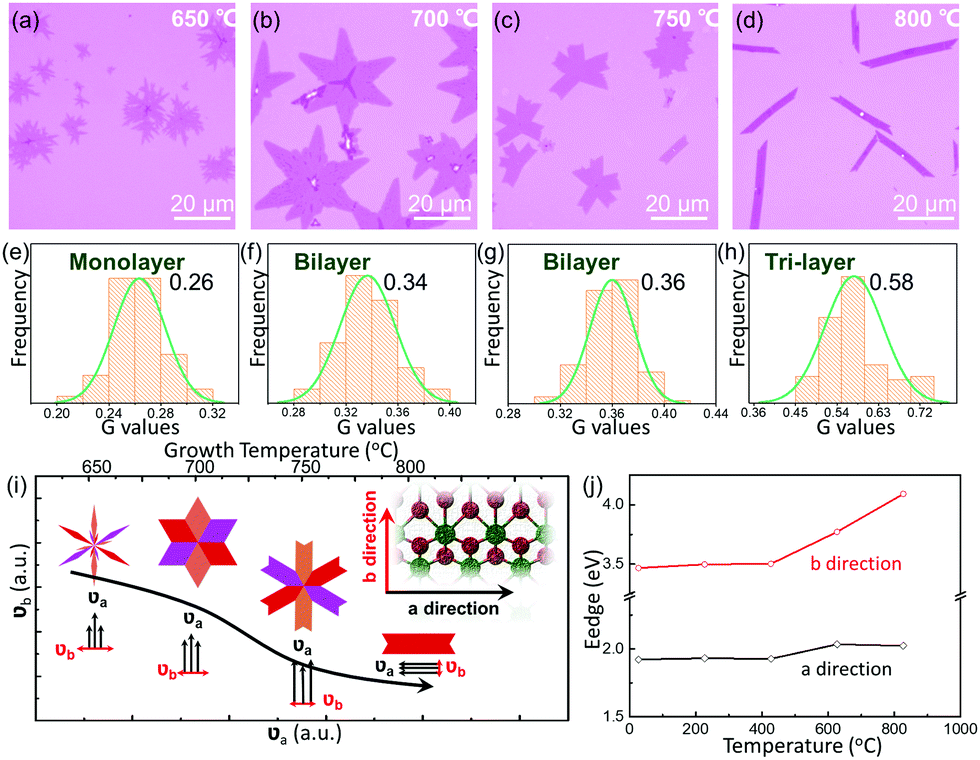 | ||
| Fig. 3 Temperature-dependent anisotropic growth behavior of 1T′ MoTe2. (a–d) Morphological evolution of the growth temperature of 1T′ MoTe2 crystals at 650 °C, 700 °C, 750 °C, and 800 °C, respectively. (e–h) The related optical contrast of the G channel of as-synthesized 1T′ MoTe2 from 650 °C to 800 °C. (i) Schematic of the morphology and growth rate in two directions of evolution (υa and υb) with the increase in growth temperature. The insets are the ball-and-stick model of 1T′ MoTe2 nanoribbons. (j) The calculation results of the relationship between edge energy (Eedge) for both directions and growth temperature. | ||
To study the dynamic growth rate of anisotropic 1T′ MoTe2, we investigated the edge stability of nanoribbons at different temperatures. The higher edge energies imply lower possibilities that atoms can grow along the direction, namely, lower growth rate. The edge energy Eedge is defined as:
| Eedge = (Eribb − E2D)/n | (1) |
The 1T′ MoTe2-based devices were fabricated by electron beam lithography. The Cr/Au electrode was prepared by heat evaporation, as shown in Fig. 4a. In Fig. 4b, the Ids–Vds curves of tri-layer 1T′ MoTe2 before and after laser (532 nm) illumination both show a straight line, while the slope is changed. The results well proved that 1T′ MoTe2 is a semi-metallic material with a photoelectric response mechanism.28–30Fig. 4c shows the photo-response (532 nm, 980 nm and 1550 nm) of the 1T′ MoTe2 device as a function of illumination time at different laser wavelengths and powers at Ids = 5 V. In addition, the photo-responses of the as-shown devices are strongly dependent on the power intensity of incident light, while all of the photocurrents at different wavelengths are increased as the laser power increased. Fig. 4d shows photocurrent (Iph) as a function of laser power (P) by fitting it with the equation Iph = αPθ at 532 nm, 980 nm and 1550 nm, respectively. The fitting values of θ are around at 1.17, 1.07, and 0.98, respectively. The responsivity (R) is defined as the photocurrent generated per unit power of incident light on the channel area, estimated to be 792 mA W−1, 379, and 287 mA W−1, respectively. The response and decay time of 1T′ MoTe2 devices under 532 nm illumination are 5.2 s and 4.3 s, respectively. To compare with other two-dimensional materials, the statistical data of some materials are shown in Table S1 (ESI†). To explore the response mechanism of few-layer 1T′ MoTe2 devices, the temperature-dependent Ids–Vds curves were measured (Fig. 4f). The slope of the Ids–Vds curves increased when the temperature of the devices increased in a dark environment, which means that few-layer 1T′ MoTe2 worked as a thermistor here. The results indicated that the photo-radiation effect should be the dominant mechanism in the few-layer 1T′ MoTe2 photodetectors.31–33 In addition, it may be the specific reason for the response time in seconds for 1T′ MoTe2-based photodetectors.34,35
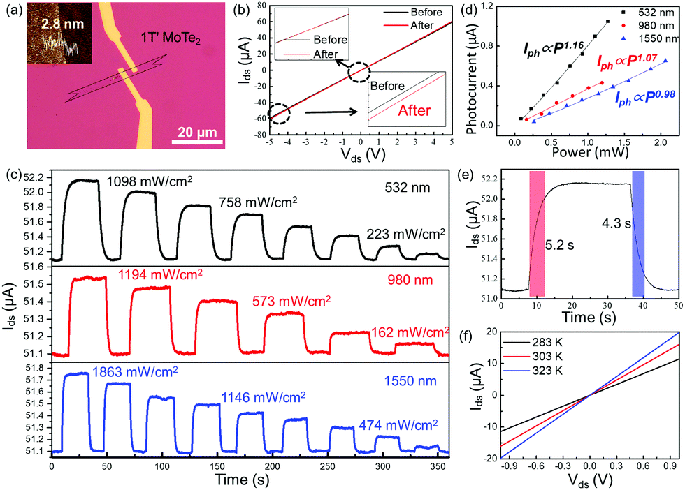 | ||
| Fig. 4 Optoelectronic properties of the 1T′ MoTe2 device. (a) OM image of the tri-layer 1T′ MoTe2 device on 300 nm SiO2/Si, the inset is the AFM image of the 1T′ MoTe2 (tri-layers). (b) The output characteristic curve (Ids–Vds) of tri-layer 1T′ MoTe2 before and after laser (532 nm) illumination. (c) Photocurrent of the 1T′ MoTe2 devices as a function of response time under different laser wavelengths (532 nm, 980 nm, 1550 nm) and power illumination at Vds = 5 V. (d) The dependence of photocurrent against the laser power under 532 nm, 980 nm and 1550 nm. (e) The response and decay time of 1T′ MoTe2 devices under 532 nm laser. (f) The Ids–Vds curves for the excitation wavelength of 532 nm at different temperatures in a dark environment. | ||
In conclusion, we have successfully achieved controllable growth of large-area uniform 1T′ MoTe2, and using molecular sieve contrast, we can identify the layer thickness of the 1T′ MoTe2 crystal. Then, due to the different responses of the edge energies to the temperature, the growth kinetic of 1T′ MoTe2 is revealed to show an anisotropic growth mode. Finally, the 1T′ MoTe2-based photodetector shows a broad-spectrum response from 532 nm to 1550 nm. Our findings not only reveal the anisotropic growth mechanism of two-dimensional materials but also investigate the photoelectric properties for their further applications in broad-spectrum detectors.
Materials and methods
CVD growth of 1T′ MoTe2
The few-layer 1T′ MoTe2 crystals were grown by a home-made CVD system with solid powder precursors. SiO2/Si silicon with a 280 nm thick SiO2 layer was used as the substrate. Mixed MoO3 (10 mg) and NaCl (1 mg) were put into a ceramic boat in the center of a tube furnace. In addition, the molecular sieves with a hole size around 4 Å were put on the surface of the mixed MoO3 powder. Then, 100 mg of tellurium powder was placed upstream to supply the Te precursor. Mixed hydrogen (H2, 10 sccm) and argon (Ar, 20 sccm) were both used as carrier gases. The samples were synthesized in a quartz tube at a temperature ranging from 650 °C to 800 °C with a growth time of 10 min. Finally, the furnace cooled down to room temperature naturally.Transfer of the CVD-synthesized 1T′ MoTe2
A thin film of polymethyl methacrylate (PMMA) was spin-coated on the substrate with MoTe2 crystals, and then baked at 130 °C for 3 min. Then, the substrate was etched in a KOH solution (1 M) at 60 °C. After lift-off, the PMMA/MoTe2 film was transferred into deionized water to wash away the residual contaminants, and then the process was continued using the TEM gird to fish out the above-mentioned film from deionized water. Finally, the transferred sample was heated at 80 °C for 30 min to evaporate water, and then dropped into acetone to wash away the PMMA coating layers.Conflicts of interest
There are no conflicts to declare.Acknowledgements
This work was supported by the National Natural Science Foundation of China (51802266, 51903208, 11872309), the Research Funds for Interdisciplinary Subject of NWPU (19SH0304), the Fundamental Research Funds for the Central Universities (310201911cx018, G2018KY0321), the Shaanxi's Key Project of Research and Development Plan (2018KA110052), the Natural Science Basic Research Plan in Shaanxi Province of China (2018JQ5192), the Science and Technology Program of Shaanxi Province (2017KJXX-16).References
- T. Chang, S. Xu, G. Chang, C. Lee, S. Huang, B. Wang, G. Bian, H. Zheng, D. Sanchez, I. Belopolski, N. Alidoust, M. Neupane, A. Bansil, H. T. Jeng, H. Lin and M. H. Zahid, Nat. Commun., 2016, 7, 10639 CrossRef PubMed.
- Y. Chang, S. Yang, C. Lin, C. Chen, C. Lien, W. Jian, K. Ueno, Y. W. Suen, K. Tsukagoshi and Y. Lin, Adv. Mater., 2018, 30, 1706995 CrossRef PubMed.
- L. Li, W. Han, L. Pi, P. Niu, J. Han, C. Wang, B. Su, H. Li, J. Xiong, Y. Bando and T. Zhai, InfoMat., 2019, 1, 54–73 CrossRef.
- S. Xu, I. Belopolski, N. Alidoust, M. Neupane and G. Bian, et al., Discovery of a Weyl fermion semi-metal and topological Fermi arcs, Science, 2015, 349, 613–617 CrossRef CAS.
- X. Cui, G. H. Lee, Y. D. Kim, G. Arefe, P. Huang, C. H. Lee, D. A. Chenet, X. Zhang, L. Wang, F. Ye, F. Pizzocchero, B. S. Jessen, K. Watanabe, T. Taniguchi, D. A. Muller, T. Low, P. Kim and J. Hone, Nat. Nanotechnol., 2015, 10, 534–540 CrossRef CAS.
- Y. Ding, N. Zhou, L. Gan, X. Yan, R. Wu, I. H. Abidi, A. Waleed, J. Pan, X. Ou, Q. Zhang, M. Zhuang, P. Wang, X. Pan, Z. Fan, T. Zhai and Z. Luo, Nano Energy, 2018, 49, 200–208 CrossRef CAS.
- S. Yuan, X. Luo, H. L. Chan, C. Xiao, Y. Dai, M. Xie and J. Hao, Nat. Commun., 2019, 10, 1775 CrossRef.
- X. Qian, J. Liu, L. Fu and J. Li, Science, 2014, 346, 1344–1347 CrossRef CAS.
- Y. Qi, P. Naumov, M. Ali, C. R. Rajamathi, W. Schnelle, O. Barkalov, M. Hanfland, S. C. Wu, C. Shekhar, Y. Sun, V. Suss, M. Schmidt, U. Schwarz, E. Pippel, P. Werner, R. Hillebrand, T. Forster, E. Kampert, S. Parkin, R. J. Cava, C. Felser, B. Yan and S. A. Medvedev, Nat. Commun., 2016, 7, 11038 CrossRef CAS.
- D. H. Keum, S. Cho, J. H. Kim, D. H. Choe, H. J. Sung, M. Kan, H. Kang, J. Y. Hwang, S. W. Kim, H. Yang, K. J. Chang and Y. H. Lee, Nat. Phys., 2015, 11, 482–486 Search PubMed.
- C. Ko, Y. Lee, Y. Chen, J. Suh, D. Fu, A. Suslu, S. Lee, J. D. Clarkson, H. S. Choe, S. Tongay, R. Ramesh and J. Wu, Adv. Mater., 2016, 28, 2923–2930 CrossRef CAS.
- Y. Liu, J. Guo, Q. He, H. Wu, H. Cheng, M. Ding, I. Shakir, V. Gambin, Y. Huang and X. Duan, Nano Lett., 2017, 17, 5495 CrossRef CAS.
- X. Ma, P. Guo, C. Yi, Q. Yu, A. Zhang, J. Ji, Y. Tian, F. Jin, Y. Wang, K. Liu, T. Xia, Y. Shi and Q. Zhang, Phys. Rev. B: Condens. Matter Mater. Phys., 2016, 94, 214105 CrossRef.
- T. A. Empante, Y. Zhou, V. Klee, A. E. Nguyen, I. H. Lu, M. D. Valentin, S. A. Naghibi Alvillar, E. Preciado, A. J. Berges, C. S. Merida, M. Gomez, S. Bobek, M. Isarraraz, E. J. Reed and L. Bartels, ACS Nano, 2017, 11, 900 CrossRef CAS.
- C. H. Naylor, W. M. Parkin, J. Ping, Z. Gao, Y. Zhou, Y. Kim, F. Streller, R. W. Carpick, A. M. Rappe, M. Drndic, J. M. Kikkawa and A. T. Johnson, Nano Lett., 2016, 16, 4297–4304 CrossRef CAS.
- J. C. Park, S. J. Yun, H. Kim, J. H. Park, S. H. Chae, S. J. An, J. G. Kim, S. M. Kim, K. K. Kim and Y. H. Lee, ACS Nano, 2015, 9, 6548–6554 CrossRef CAS.
- K. Chen, Z. Chen, X. Wan, Z. Zheng, F. Xie, W. Chen, X. Gui, H. Chen, W. Xie and J. Xu, Adv. Mater., 2017, 29, 1700704 CrossRef.
- L. Zhou, A. Zubair, Z. Wang, X. Zhang, F. Ouyang, K. Xu, W. Fang, K. Ueno, J. Li, T. Palacios, J. Kong and M. S. Dresselhaus, Adv. Mater., 2016, 28, 9526–9531 CrossRef CAS PubMed.
- L. Yang, W. Zhang, J. Li, S. Cheng, Z. Xie and H. Chang, ACS Nano, 2017, 11, 1964–1972 CrossRef CAS.
- Q. Zhang, Y. Xiao, T. Zhang, Z. Weng, M. Zeng, S. Yue, R. G. Mendes, L. Wang, S. Chen, M. H. Rümmeli, L. Peng and L. Fu, Chem. Mater., 2017, 29, 4641–4644 CrossRef CAS.
- J. Zhou, F. Liu, J. Lin, X. Huang, J. Xia, B. Zhang, Q. Zeng, H. Wang, C. Zhu, L. Niu, X. Wang, W. Fu, P. Yu, T. Chang, C. H. Hsu, D. Wu, H. T. Jeng, Y. Huang, H. Lin, Z. Shen, C. Yang, L. Lu, K. Suenaga, W. Zhou, S. T. Pantelides, G. Liu and Z. Liu, Adv. Mater., 2017, 29, 1603471 CrossRef.
- H. Zhu, Q. Wang, L. Cheng, R. Addou, J. Kim, M. J. Kim and R. M. Wallace, ACS Nano, 2017, 11, 11005–11014 CrossRef CAS PubMed.
- J. Wang, X. Luo, S. Li, I. Verzhbitskiy, W. Zhao, S. Wang, S. Y. Quek and G. Eda, Adv. Funct. Mater., 2017, 27, 1604799 CrossRef.
- L. Zhou, S. Huang, Y. Tatsumi, L. Wu, H. Guo, Y. Q. Bie, K. Ueno, T. Yang, Y. Zhu, J. Kong, R. Saito and M. Dresselhaus, J. Am. Chem. Soc., 2017, 139, 8396–8399 CrossRef CAS PubMed.
- M. Zhu, Y. Zhao, Q. Feng, H. Lu, S. Zhang, N. Zhang, C. Ma, J. Li, J. Zheng, J. Zhang, H. Xu, T. Zhai and J. Zhao, Small, 2019, 15, 1903159 CrossRef CAS PubMed.
- Q. Feng, N. Mao, J. Wu, H. Xu, C. Wang, J. Zhang and L. Xie, ACS Nano, 2015, 9, 7450–7455 CrossRef CAS PubMed.
- F. Cui, C. Wang, X. Li, G. Wang, K. Liu, Z. Yang, Q. Feng, X. Liang, Z. Zhang, S. Liu, Z. Lei, Z. Liu, H. Xu and J. Zhang, Adv. Mater., 2016, 28, 5019–5024 CrossRef CAS PubMed.
- D. Qu, X. Liu, M. Huang, C. Lee, F. Ahmed, H. Kim, R. S. Ruoff, J. Hone and W. J. Yoo, Adv. Mater., 2017, 29, 1606433 CrossRef PubMed.
- J. H. Sung, H. Heo, S. Si, Y. H. Kim, H. R. Noh, K. Song, J. Kim, C. S. Lee, S. Y. Seo, D. H. Kim, H. K. Kim, H. W. Yeom, T. H. Kim, S. Y. Choi, J. S. Kim and M. H. Jo, Nat. Nanotechnol., 2017, 12, 1064–1070 CrossRef CAS PubMed.
- Z. Lin, J. Wang, X. Guo, J. Chen, C. Xu, M. Liu, B. Liu, Y. Zhu and Y. Chai, InfoMat., 2019, 1, 242–250 CrossRef.
- D. Zheng, H. Fang, M. Long, F. Wu, P. Wang, F. Gong, X. Wu, J. C. Ho, L. Liao and W. Hu, ACS Nano, 2018, 12, 7239–7245 CrossRef CAS PubMed.
- X. Lu, P. Jiang and X. Bao, Nat. Commun., 2019, 10, 138 CrossRef.
- K. Zhang, T. Zhang, G. Cheng, T. Li, S. Wang, W. Wei, X. Zhou, W. Yu, Y. Sun, P. Wang, D. Zhang, C. Zeng, X. Wang, W. Hu, H. Fan, G. Shen, X. Chen, X. Duan, K. Chang and N. Dai, ACS Nano, 2016, 10, 3852–3858 CrossRef CAS.
- L. Jiao, W. Jie, Z. Yang, Y. Wang, Z. Chen, X. Zhang, W. Tang, Z. Wu and J. Hao, J. Mater. Chem. C, 2019, 7, 2522–2529 RSC.
- Z. Yang and J. Hao, Adv. Mater. Technol., 2019, 1900108 CrossRef.
Footnotes |
| † Electronic supplementary information (ESI) available. See DOI: 10.1039/d0nh00075b |
| ‡ X. J. Wang, J. Shang, and M. J. Zhu were contributed equally to this work. |
| This journal is © The Royal Society of Chemistry 2020 |