
 Open Access Article
 This Open Access Article is licensed under a Creative Commons Attribution-Non Commercial 3.0 Unported Licence
Metal assisted chemical etching of silicon in the gas phase: a nanofabrication platform for X-ray optics†
Lucia
Romano
 *abc,
Matias
Kagias
a,
Joan
Vila-Comamala
ab,
Konstantins
Jefimovs
ab,
Li-Ting
Tseng
a,
Vitaliy A.
Guzenko
a and
Marco
Stampanoni
ab
*abc,
Matias
Kagias
a,
Joan
Vila-Comamala
ab,
Konstantins
Jefimovs
ab,
Li-Ting
Tseng
a,
Vitaliy A.
Guzenko
a and
Marco
Stampanoni
ab
aPaul Scherrer Institut, 5232 Villigen PSI, Switzerland. E-mail: lucia.romano@psi.ch
bInstitute for Biomedical Engineering, University and ETH Zürich, 8092 Zürich, Switzerland
cDepartment of Physics and CNR-IMM-University of Catania, 64 via S. Sofia, Catania, Italy
First published on 17th February 2020
Abstract
High aspect ratio nanostructuring requires high precision pattern transfer with highly directional etching. In this work, we demonstrate the fabrication of structures with ultra-high aspect ratios (up to 10![[thin space (1/6-em)]](https://www.rsc.org/images/entities/char_2009.gif) 000:1) in the nanoscale regime (down to 10 nm) by platinum assisted chemical etching of silicon in the gas phase. The etching gas is created by a vapour of water diluted hydrofluoric acid and a continuous air flow, which works both as an oxidizer and as a gas carrier for reactive species. The high reactivity of platinum as a catalyst and the formation of platinum silicide to improve the stability of the catalyst pattern allow a controlled etching. The method has been successfully applied to produce straight nanowires with section size in the range of 10–100 nm and length of hundreds of micrometres, and X-ray optical elements with feature sizes down to 10 nm and etching depth in the range of tens of micrometres. This work opens the possibility of a low cost etching method for stiction-sensitive nanostructures and a large range of applications where silicon high aspect ratio nanostructures and high precision of pattern transfer are required.
000:1) in the nanoscale regime (down to 10 nm) by platinum assisted chemical etching of silicon in the gas phase. The etching gas is created by a vapour of water diluted hydrofluoric acid and a continuous air flow, which works both as an oxidizer and as a gas carrier for reactive species. The high reactivity of platinum as a catalyst and the formation of platinum silicide to improve the stability of the catalyst pattern allow a controlled etching. The method has been successfully applied to produce straight nanowires with section size in the range of 10–100 nm and length of hundreds of micrometres, and X-ray optical elements with feature sizes down to 10 nm and etching depth in the range of tens of micrometres. This work opens the possibility of a low cost etching method for stiction-sensitive nanostructures and a large range of applications where silicon high aspect ratio nanostructures and high precision of pattern transfer are required.
New conceptsWhat is the difference between microfabrication and nanotechnology? Scientists struggle all around the world to scale down the device feature size by top down techniques such as plasma etching with specialized cryogenic gases and electrode design. However, a bottom up approach is again the natural and cost effective choice of nanofabrication. In this regard, metal assisted chemical etching bypasses the limits of aspect ratio with a local electrochemical reaction that occurs only at the nanoscale of the catalyst surface. We propose the concept of inducing the MacEtch reaction in the gas phase in order to promote MacEtch among the dry etching techniques. The new method allows vertical etching with the extreme aspect ratio of 10000:1 and feature size down to 10 nm with high precision and control of pattern transfer into the silicon substrate. Such capability opens a new world of possibilities for nanofabrication. As a proof-of-concept, we successfully etched patterned structures for X-ray optics, where the control of feature size, roughness and precision of pattern transfer are fundamental for the performances of the application.
|
Since its discovery in 2000 by Li et al.1 metal assisted chemical etching (MacEtch) has emerged as a new technique capable of fabricating 3D nano- and micro-structures of several shapes and applications such as nanoporous layers, nanowires, 3D objects, MEMS, microfluidic channels, vias, X-ray optics, and sensor devices in a few semiconductors – Si, Ge, poly-Si, GaAs,2 and SiC3 – and using different catalysts – Ag, Au, Cu, Pt, and Pd.2 In typical MacEtch, a metal (the cathode) patterned silicon (the anode) is in contact with a solution of HF and H2O2 (the electrolyte) and a local electrochemical etching occurs. The metal serves as a catalyst for H2O2 reduction with consequent hole injection deep into the valence band of the silicon.1 The concentration of holes becomes higher in the region surrounding the metal catalyst, where silicon is readily oxidized by HF and forms silicon fluoride compounds, and the reaction continues as the catalyst is pulled down into the substrate. H2O2 is by far the most commonly employed oxidizer in MacEtch,4 but other oxidizers can be employed, such as HNO35 or even O2.6
MacEtch in liquid demonstrated the capability to etch nanostructures with a very high aspect ratio, such as nanowires (NWs). However, as a wet etching technique, it suffers from stiction and agglomeration of structures during drying due to van der Waals and capillary forces7 between adjacent surfaces at the interface between liquid and air. The NW agglomeration is highly undesirable and considered as a limiting factor for all the applications where the surface is directly related to the device efficiency, such as solar cells or sensing devices. Indeed, large bundles prevent conformal coating, deteriorate the optical properties of the array, and may induce higher series resistance. For this reason, post etching drying steps, such as CO2 based critical point drying are usually required.
In 2014, two independent papers8,9 demonstrated that a MacEtch reaction could occur by evaporating and condensing the electrolyte on the surface of a metal patterned silicon. Hu et al.8 demonstrated that the MacEtch reaction occurs at room temperature in the presence of aerated HF in a similar fashion of metal corrosion by air. The oxygen diffusion through the condensed HF/water layer limits the etching rate and the maximum etched depth, so a maximum depth of 6 μm was etched in 3 h. According to Hildreth et al.,9 the electrolyte is evaporated from a liquid solution containing HF and H2O2 and forms a condensed thin layer where the MacEtch reaction occurs. In this paper, MacEtch was induced without H2O2 in a gas–solid reaction by exposing the metal patterned silicon to a vapour of HF and a continuous flow of air. Limiting the water content of the solution and warming up the substrate (40–55 °C) effectively reduced the liquid condensation enabling a gas–solid reaction to occur at the metal catalyst. As a consequence, the stiction of the etched nanostructures due to the liquid drying was effectively minimized.
We report the etching of very deep (up to 107 μm) nanostructures (vertically aligned nanowires with section size in the range of 10–100 nm) in the 〈100〉 direction of the Si substrate with a very high aspect ratio (up to 10000:1) and high etching rate (up to 25 μm h−1). We investigated the use of platinum as an effective stable catalyst thanks to the formation of Pt silicide on the Si substrate. We etched some lithographic patterns consisting of X-ray optical elements to demonstrate the feasibility of pattern transfer with high resolution and fidelity, with etching perpendicular to the Si wafer and a sharp surface in the trenches. A schematic of the process is reported in Fig. 1.
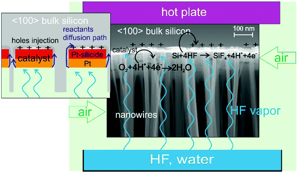 | ||
| Fig. 1 Schematic of MacEtch to produce Si nanostructures in a gas phase reaction. The metal patterned Si substrate is suspended above a liquid solution of water diluted HF and warmed up. The gas etchant (HF) is produced by evaporation of the water diluted HF solution, the oxidizer O2 is supplied by the continuous flow of air, O2 is reduced at the metal and charge carriers are injected into Si, and HF oxidizes Si underneath the metal. The catalyst is platinum and the formation of Pt silicide stabilizes the pattern so the etching proceeds along the 〈100〉 direction of the Si substrate. The SEM image shows the cross section at the base of etched Si nanowires where the active catalyst sinks into the Si substrate. | ||
The method is an interesting and promising cost effective technology for producing high aspect ratio nanostructures by surpassing the limits of other gas phase etching techniques in the nanoscale, such as reactive ion etching.10–12 Several research fields, such as photonics,13,14 microfluidics,15 bioengineering,16 thermoelectric materials,17 batteries,18,19 solar cells,20,21 sensors and MEMS22 can take advantage of using MacEtch in the gas phase as nano- and micro-fabrication techniques. Here, we highlight our work by focusing on the fabrication of X-ray diffractive optical elements. The applicability of such optics spans from medical applications, such as breast phase contrast imaging23 and dark-field lung imaging24 with potentially improved diagnostic power, to high end imaging at the nanoscale with highly brilliant light sources.25,26
Results and discussion
Pt catalyst pattern for nanowire fabrication
Nanostructures can be fabricated by bottom-up and top-down approaches. For example, nanowires can be grown bottom-up by a vapour–liquid–solid (VLS) reaction27 or top-down etched by gas28 and wet etching techniques.1 In both approaches, an ordered array requires a dedicated pattern of metal nanoparticles for the VLS or etching mask, respectively. The patterning of nanostructures requires high precision pattern transfer and high lateral resolution during growth or etching, and with MacEtch in liquid this corresponds to a condition of very high HF concentration.29 A gold catalyst suffers from bad adhesion on silicon substrates, yet a detrimental pattern peel-off has been reported during MacEtch in conditions of high HF concentration.30,31 On the other hand, uniform high aspect ratios have been reported for a nanoporous Au catalyst in conditions of low HF and high H2O2 concentration.32,33 Under these conditions the etching is more isotropic,34 the tops of the trenches appear wider with respect to the bottom compromising the fidelity of the pattern in the lateral dimension, so the process is not suitable for high aspect ratio nanostructures.We used 〈100〉 n-type Si wafer as a substrate and Pt thin film as a catalyst. There are very few data in the literature about the use of Pt as a MacEtch catalyst, it has been mostly investigated in the form of nanoparticles35–39 or added as a top layer of Au thick film.40 Pt has the advantage of forming a stable silicide (PtSi and Pt2Si) on Si surfaces at relatively low temperature (180–400 °C). The Pt silicide ensures a robust adhesion of the metal to the Si substrate during MacEtch in conditions of high HF concentration. Since the etching rate decreases with decreasing the oxidant concentration,32 an effective catalyst must be chosen to maximize the etching reactivity in conditions of low oxidant concentration. Platinum has a faster reported etching rate for MacEtch37 due to its superior catalytic activity. Here, we implemented a self-assembly nanostructured pattern32,41 of a Pt thin film by using electron beam evaporation and thermal de-wetting (400–550 °C). A metal film de-wetting process was reported as a lithography-free method to fabricate Si nanowires by MacEtch in liquid solution of HF and H2O2.42 We used the de-wetting of the Pt nanopattern to produce a simple etching pattern to fabricate Si nanowires with a section size in the range of 10 to 100 nm by MacEtch in the gas phase. The use of an interconnected pattern has been demonstrated to effectively reduce the off-vertical catalyst movement.29,32,33 De-wetting occurs when a thin film on a solid substrate is heated, inducing clustering of the film.41 The film structure morphology (feature size, roughness, pores distribution) and the pattern evolution strongly depend on the film/substrate parameters (film material, film thickness, substrate material, defects) and the experimental conditions (deposition rate, annealing temperature, annealing environment etc.). The Pt de-wetting was investigated for Pt film thicknesses in the range of 8–20 nm and in the temperature range between 250 and 600 °C for a 30 min annealing in air to find the best conditions for a robust interconnected pattern of the MacEtch catalyst. The Pt film was evaporated on the Si substrate with native oxide (SiOX). This is because de-wetting of metals is favoured on insulator substrates,41 while higher temperature and longer annealing processes are required on Si surfaces.43,44 De-wetting occurred for Pt thin films on native Si oxide surfaces in agreement with the literature,45 whilst no de-wetting was observed under the same experimental conditions when the native oxide was removed by dipping the substrate in HF immediately before the platinum deposition.
Pt silicide formation has been extensively reported in the literature; the Pt2Si phase forms at lower temperatures (180–200 °C) and this is followed by the formation of the PtSi (280–400 °C) phase at higher temperatures.46–48 Pt silicide has been reported to form also in the presence of a native silicon oxide layer.45,48 This is a relevant characteristic of the Pt–Si system that enables self-assembled nanopattern formation through the de-wetting process on native Si oxide with a robust substrate adhesion due to the Pt silicide formation. If the annealed sample is dipped in water diluted HF (2–10 wt%), the metal film is lifted off starting from the edges of the pattern, since Pt and Pt silicide are not etched in HF, this indicates that there is still some residual native Si oxide layer at the interface between Si and Pt. The formation of a top layer of SiO2 is possible49,50 in the case of annealing in oxidizing ambient. However, when the sample is dipped in 30 wt% H2O2 an immediate vigorous bubble formation takes place. This indicates that H2O2 decomposition with O2 release is due to the presence of a pure Pt surface on top of the de-wetted metal. According to the literature and our experimental observations, the metal layer has most likely the structure reported in Fig. 2a: film de-wetting occurs forming a self-assembled nanopattern with a top layer of Pt and a layer of Pt silicide (PtSi and Pt2Si) above a residual native Si oxide layer on the substrate. The film composition (Fig. 2a) is supported by X-ray photoelectron spectroscopy (see the Fig. S1, ESI†). The de-wetting occurs with fracturing and reassembling of the metal film in a metal network such as the one reported in the SEM plan view of Fig. 2b. The interpretation of SEM contrast in Fig. 2b is supported by the backscattering electron image (see the Fig. S2, ESI†) and the energy dispersive X-ray spectroscopy (Fig. S3, ESI†). The growth of asymmetric holes during de-wetting (Fig. 2b) is also an indication of Pt silicide formation.45
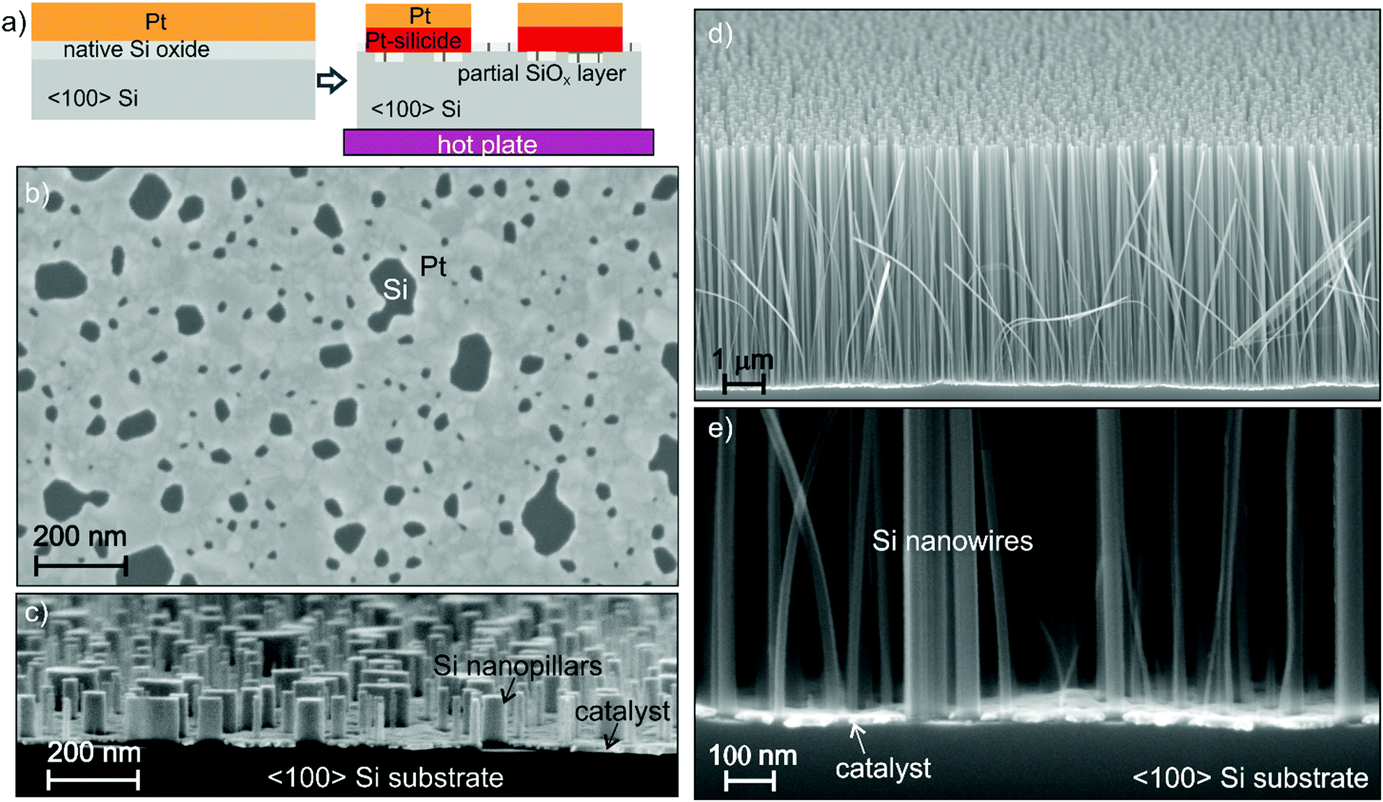 | ||
| Fig. 2 (a) Schematics of the Pt thin film on the Si substrate and its evolution during thermal de-wetting: a thin layer of Pt silicide is formed at the interface between a Pt top layer and the oxygen terminated Si surface of the substrate; (b) SEM plan view of the 12 nm Pt film after thermal annealing at 550 °C (Pt has brighter contrast, the de-wetting forms pores in the Pt layer); (c) SEM cross section after 10 min of MacEtch in the gas phase; (d) SEM cross section after 1 h of etching; (e) magnified image of the bottom nanowires, where the metal catalyst has brighter contrast than Si. | ||
The de-wetting of the Pt nanopattern produced at 550 °C (Fig. 2b) was used to fabricate Si nanowires with a section size in the range of 10 to 100 nm. Pt (12 nm) was deposited on a 〈100〉 Si substrate and annealed at 550 °C. Samples of 1 × 1 cm2 were cut from the wafer and held approximately 2 cm above the water diluted HF solution by means of an HF-compatible static chuck with substrate temperature control. The sample holder is suspended above the liquid in order to allow continuous flow of air into the chamber to access the metal pattern. The HF vapour is produced by the water diluted HF solution at 25 °C. Air in continuous flow provides the necessary oxidizer amount to perform the MacEtch in the gas phase.
The surface morphology variation can be observed by eye after a few minutes of exposure to HF vapour and air, with a progressive opaquing of the mirroring surface as a function of the exposure time. MacEtch is essentially a highly localized electrochemical etching reaction: the catalyst pattern progressively sinks down into the silicon and a uniform carpet of nanopillars (Fig. 2c) and nanowires (Fig. 2d) is formed. The catalyst film at the bottom of the NW carpet (Fig. 2e) is flat and stable, indicating that the etching direction is perpendicular to the Si substrate with a very good control of the side wall slope (the bending of a few NWs is due to the cleavage of the Si substrate for the cross section preparation). We would like to stress that the stability of the catalyst pattern is due to the formation of Pt silicide during the thermal de-wetting step. Without the thermal treatment the catalyst layer strongly corrugates and breaks after 2–3 μm of etching (see the Fig. S4, ESI†). The etching fidelity in the lateral dimension can be observed by comparing the feature size of the original pattern and the resulting NWs (see Fig. 2b and c, SEM images in plan view and cross section have the same magnification). The NWs appear to be separated, meaning that the NW agglomeration has been definitively reduced with respect to the liquid MacEtch process7 (see the Fig. S5, ESI†). The NW cross section has been measured in several high magnification SEM images at the bottom of the carpet (Fig. 2e) and in plan view, the NWs have a section size in the range of 10–100 nm, in close correspondence with the size distribution of the holes in the initial Pt pattern.
A carpet of nanowires is useful for all the nanotechnology applications where silicon is required with a high surface/volume aspect ratio, such as black silicon for solar cells,21 thermoelectrics17 or battery anodes.18 Moreover, nanowires can be used as diffractive optics in speckle based X-ray phase contrast imaging.51 Nanowires are expected to improve the sensitivity by producing speckles of smaller size in comparison to sandpaper52 or other membranes with feature size in the micrometre scale.
Etching mechanism
The liquid composition was varied by mixing HF (49 wt%) and deionized water in different volume ratios with a total liquid volume of 100 ml. The higher the HF concentration the higher the supply of electrolyte (HF and water) to reach the catalyst and etch silicon. Since the etching chamber is not hermetically closed and the system is placed on a bench under air in laminar flow, the air is continuously flowed in during the etching. The evaporation rate of a liquid also increases if the surrounding air is moving, so the air flow also raises the evaporation rate of HF. The oxygen present in the air reacts mainly on the Pt surface, and the main cathodic reaction is the following eqn (1)| O2 + 4H+ + 4e− → 2H2O | (1) |
The etching rate was studied as a function of HF concentration and temperature. The etching rate was measured on samples of 1 × 1 cm2 over a period of 2 hours, and the NW carpet thickness was measured by SEM in cross section in the centre of the square. Fig. 3a shows the etching rate for different HF molar concentrations in the liquid solution of HF and water as a function of the substrate temperature in the range between 35 and 55 °C. Since the liquid is kept at room temperature, we assume the source of etchants is constant. The etching rate should result from the increase with the temperature of the MacEtch reactivity and the etchant depletion with the temperature due to the desorption rate at the substrate. However, the etching rate versus temperature does not reveal a simple trend. The etching with the highest HF concentration is reminiscent of the volcano plot observed by Hildreth et al.9 The volcano plot was reported for vapour HF etching of SiO2 but it has a maximum at lower temperature (30 °C).53 The etching in the gas-phase region takes place via a slow gas–solid reaction that is catalysed by the adsorbed moisture on the sample surface in a condensed thin layer less than 2 nm thick.9 The presence of H2O enhances the ionization reaction of HF molecules, resulting in an increase of HF2− ions that are more reactive to dissolve SiO2, according to eqn (2):54
| SiO2 + 2HF2− + 2HF → SiF62− + 2H2O | (2) |
| Si + 4h+ + 4HF → SiF4 + 4H+ | (3) |
| Si + 2H2O + 4h+ → SiO2 + 4H+ | (4) |
 | ||
| Fig. 3 (a) Graph showing etching rate vs. substrate temperature after 2 h etching time at different HF molar concentrations (mol l−1) of the water diluted solution; (b) SEM cross section of etched nanowires and the edge of the pattern; (c) nanowire length variation between the edge and the centre of the sample as a function of the substrate temperature; (d) etching rate at a substrate temperature of 55 °C as a function of HF molar concentration of the water diluted HF solution, the etching time is 2 h; (e) SEM cross section of nanowires etched in 4 h at HF molar concentration of 28 mol l−1 and substrate temperature of 55 °C; (f) SEM plan view of nanowires in (e); (g) high magnification SEM of the bottom part of the nanowire carpet in (e); (h and i) high magnification SEM of the top part of the nanowire carpet in (e). | ||
The etching proceeds with higher etching rate at the border of the pattern, an example of this effect is visible in Fig. 3b. We measured the NW carpet thickness in the centre of the sample and at the border. Fig. 3c shows the relative variation of the carpet thickness (ΔL) as a function of the substrate temperature; the higher the temperature the smaller the ΔL. ΔL is the variation of thickness with respect to the centre, the sample size is 1 × 1 cm2, so the edge-to-centre distance is about 0.5 cm. However, the main variation is observed a few hundred micrometres from the edge, as shown in Fig. 3b. Some border effects have been reported also in wet-MacEtch: Chen et al. observed a variation of etching direction going from the border to the centre as a consequence of different diffusion flux at the border;63 with a micropattern of an Au catalyst we experienced a kind of reverse effect, with slower etching at the border.32 In the case MacEtch in the gas phase, we observed a faster etching at the border for a pattern area of 1 cm2, while the etching is uniform for a patterned area of a few mm2. The supply of oxygen is limited during the etching and the border effect can be explained in terms of local etchant depletion. Oxygen is locally consumed when a MacEtch reaction occurs and the local concentration of oxygen is always higher at the border, the catalyst area being progressively reduced at the pattern edge. As the substrate temperature increases, the oxygen diffusion increases with a diffusion flux that is driven by the concentration gradient, smoothing the local etchant depletion in the centre and reducing the ΔL.
The best processing temperature is at 55 °C for etching uniformity, low porosity and reduced agglomeration. The etching rate at 55 °C as a function of HF molar concentration is reported in Fig. 3d. A small dip can be observed in the HF concentration range 12–18 mol l−1. The variation is within the experimental errors, however it can be speculated that this is related to the catalytic effect of water. Since water favours the HF ionization, at low HF concentration the water content could be still enough to increase the etching rate. Then, at higher HF concentration, the etching rate increase is dominated by the increase of HF content in the vapour. Relevant high etching rates of 20–25 μm h−1 are reported for very high HF concentration, these values are comparable to the wet-MacEtch. Fig. 3e and f report the SEM cross section and plan view, respectively of NWs obtained in conditions of high HF concentration with an etching time of 4 hours. Considering the original Pt de-wetting pattern (see Fig. 2b) and the high magnification SEM image of the bottom cross section (Fig. 3g), the NWs section is in the range 10–100 nm. It is possible to observe the presence of NWs with section as small as 10 nm along the full length of the etched NW carpet (see the Fig. S9, ESI†). The high magnification images (Fig. 3h and i) show the presence of structures with feature size of 10 nm even in the top part. Therefore, the nanostructures in Fig. 3e–i have an aspect ratio in the range of 1000:1 to 10000:1. This demonstrates that an aspect ratio as high as 10000:1 can be achieved by MacEtch in the gas phase.
The NWs have low agglomeration (see Fig. 3f) even at these high aspect ratios, indicating that a gas phase reaction is taking place during the whole process. Moreover, the catalyst layer at the bottom of the etched carpet (see Fig. 3e and g) is flat and stable, indicating that the etching could be continued, opening the possibility for MacEtch in the gas phase to etch extremely high aspect ratio nanostructures in silicon with very high precision and side wall slope perpendicular to the substrate.
Patterned structures for X-ray optics
With the rise of X-ray grating interferometry,64 access to phase and scattering contrasts has been granted on conventional X-ray sources,65 thus facilitating the potential for medical and industrial applications. This is achieved by utilizing gratings with micrometre sized periods that modulate the phase or the intensity of the X-rays. The key challenge faced at the moment is the fabrication of such gratings in order to deliver high contrast images over extended areas.66–68 Specifically, in the case of (bio)medical applications where the delivered dose is a critical factor, submicron periods become necessary in order to visualize the subtle differences between soft tissues.69 Taking into account that the phase or intensity modulation capability of the gratings is a function of their height/depth, it becomes evident that high aspect ratios are required for applications operating in the medical or industrial X-ray energy range. Efficiency of X-ray diffractive elements is strictly dependent on precision of the pitch and uniformity of duty cycle along the depth. This is possible only if the side wall slope of the etched structures is perpendicular to the Si wafer substrate.In the following section, we address the fabrication of Si templates that can be used directly as phase modulating gratings or be subsequently filled with high X-ray absorbing materials, such as Ir70 or Au,71 and used as analyser gratings. Patterned metal layers were produced by following the schematic procedure of Fig. 4a. The pattern was produced by using e-beam lithography in the case of nanostructures and a conventional UV lithography in the case of microstructures. The patterns of X-ray diffractive elements, consisting of linear72 or circular gratings,73 were optimized by introducing interconnects between the catalyst lines, which suppress the off-vertical catalyst movement during MacEtch.29 In detail, bridges were added to a periodic pattern, and some examples of metal patterns before the etching are reported in the ESI† (Fig. S10). We demonstrated in previous work32 that the use of a porous catalyst is necessary to uniformly etch patterns with feature sizes in the micrometre range. Therefore, we used the thermal de-wetting process of Pt to create a porous catalyst within the metal pattern. The de-wetting temperature was 400 °C to get very thin NWs inside the main trenches so that the eventual X-ray absorption during the final application is minimized.
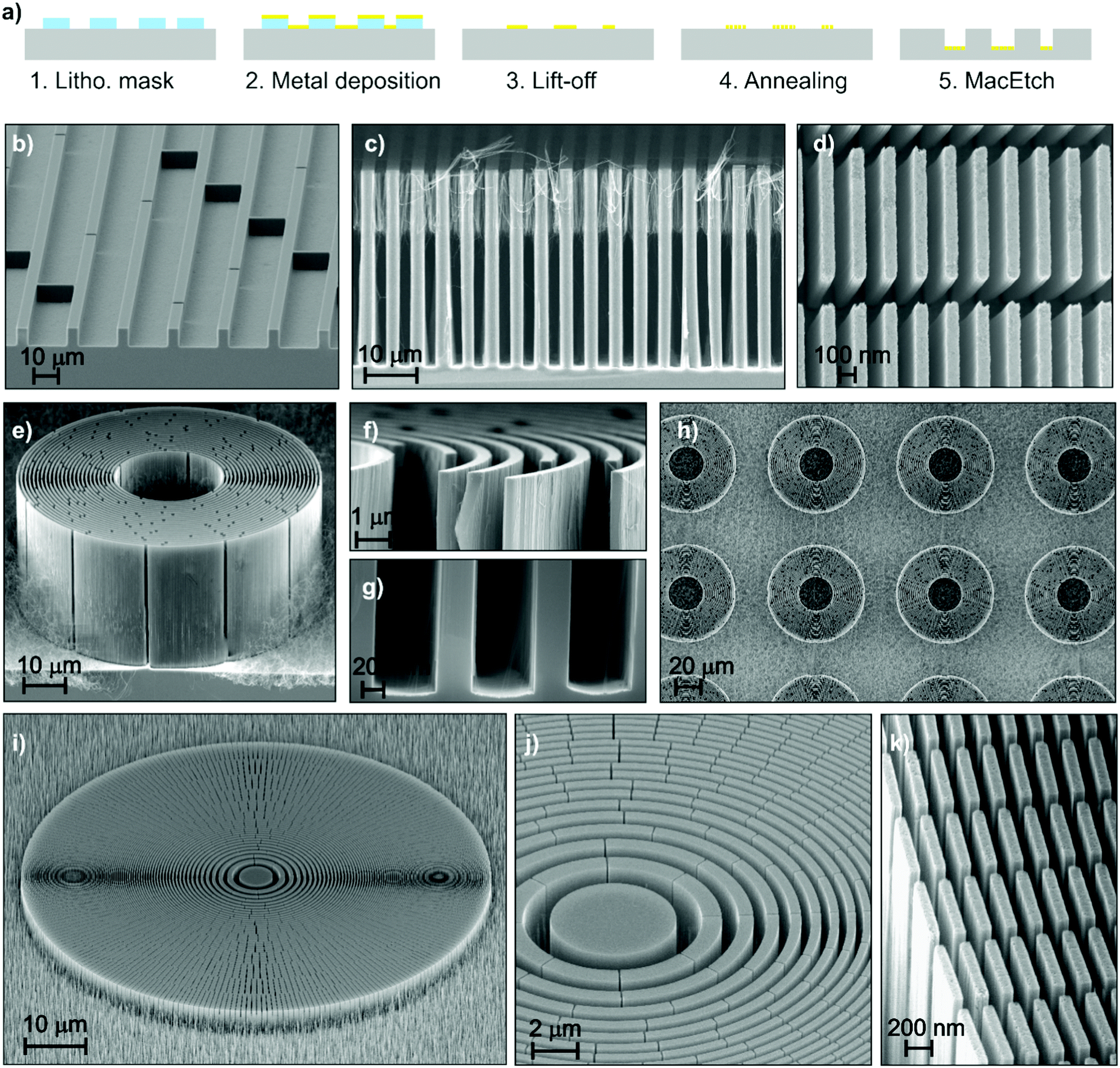 | ||
| Fig. 4 (a) Schematic of processing for patterned structures; (b) tilted view of the linear grating with pitch of 20 μm; (c) cross section of the linear grating with pitch of 4.8 μm; (d) plan view of the linear grating with pitch of 200 nm; (e) tilted view of the circular grating with pitch of 1 μm and magnified cross section view of the (f) top and (g) bottom; (h) plan view of the circular gratings array; (i) tilted view of the zone plate with outermost pitch of 200 nm and magnified view of the (j) centre and (k) border. Further details are reported in the ESI† (see Table S1). | ||
The etching solution contained HF 6 mol l−1 in order to have an etching rate in the range of 5–8 μm h−1. The main challenge of MacEtch in the gas phase to etch micro-patterns is to maintain a uniform concentration of reactants close to the metal surface during the whole process, and the main diffusion flux is perpendicular to the pattern while the etched microstructures themselves block the flux of reactant species parallel to the surface. The continuous air flow helps the reactant diffusion through the trenches and acts as gas carrier for the fresh reactive species in order to maintain a constant flux to reach the metal catalyst. The MacEtch byproducts are released as gases, and the air flow helps at the same time to remove and disperse the byproducts favouring the mass transfer. The concentration gradient grows with the etching rate, therefore etching uniformity is better for slow etching rate. This effect is less relevant for NW patterns since the etched structures have section size in the range of 10–100 nm with relatively large gap (∼100 nm) while the gratings are densely packed long trenches, that can act like microchannels for the gas diffusion of the reactive species.
Fig. 4b–k show some examples of X-ray optics structures, such as linear (Fig. 4b–d) and circular (Fig. 4e–h) gratings and zone plates (Fig. 4i–k). A linear grating (Fig. 4c) with pitch 4.8 μm was etched up to 39 μm deep (substrate temperature 40 °C). Residuals of NWs are visible in the Si trench due to the pores in the de-wetted catalyst. Fig. 4d reports the etching of a grating with a pitch size of 200 nm and line width of 80 nm (depth 10 μm), and the high resolution image confirms the pattern fidelity (see Fig. S10, ESI†).
The circular gratings (Fig. 4e–h) have a pitch of 1 μm with a duty cycle of 0.65. A depth of 29 μm was realized with substrate temperature of 55 °C and etching rate of about 7 μm h−1. The resulting aspect ratio of the Si structures is about 82:1. The smoothness of the etched Si lines is visible in the high resolution images of the grating from top (Fig. 4f) and bottom (Fig. 4g) views. In the bottom image (Fig. 4g) a weak catalyst bending is observed in the centre of the lines, and thin NWs are barely visible. The etching is very uniform on the whole patterned area (0.5 × 0.5 cm2) as demonstrated by the uniform Moiré pattern visible in the low magnification SEM plan view image (Fig. 4h). The NWs formed in the centre of the grating and in the area surrounding the grating are generated by the catalyst de-wetting at 400 °C. According to the Pt de-wetted pattern, the section size of the NWs is in the range of 10–30 nm, so the aspect ratio of the nanowires is in the range of 1000:1. We observed the uniform vertical movement of the metal pattern along the whole area. This demonstrates the capability of the technique to etch different feature sizes in the scale of 10 nm to 1 μm, with the aspect ratio in the range 10–1000:1, maintaining the etching direction along the 〈100〉 for tens of micrometres. This opens the possibility of high precision and high aspect ratio etching of complex X-ray optics, such as zone plates.29,74Fig. 4i–k show an etched zone plate with pitch size going from 2 μm to 200 nm respectively from the centre to the outermost zone. A depth of 5 μm was realized by etching the sample for 1 h at a substrate temperature of 55 °C. It is remarkable to note the precision of the pitch size and duty cycle, which are constant along the etching direction, demonstrating the high control of the etching slope that is perpendicular to the substrate.
The structures etched by gas-MacEtch appear very smooth with low Si porosity, almost visible only on the top part (see Fig. 4d and f with respect of Fig. 4g). In liquid solutions of HF and H2O2, MacEtch of heavily doped Si substrates produces very porous structures even in conditions of very low H2O2 concentration.61,75 The comparison (see the Fig. S8, ESI†) of the same structures etched by gas-MacEtch and MacEtch in liquid solution of HF and H2O2 showed that the Si porosity in gas-MacEtch of heavily doped Si is effectively reduced with respect of MacEtch in liquid.
The high aspect ratio, especially in the case of dense nanostructures in the sub-micrometre range, demonstrates the advantage of MacEtch in the gas phase with respect to the plasma etching technique. For comparison, for 100 nm features with vertical sidewalls by deep reactive ion etching process the typical reported aspect ratio is in the range of ∼30:1,11 and it is possible to achieve aspect ratios up to 60:1 at the expense of sidewall profile and duty cycle distortions.10
Conclusions
Evaporated Pt thin film has many advantages as a MacEtch catalyst, making Pt the catalyst of choice for a high aspect ratio MacEtch process. Pt forms a stable silicide during the thermal de-wetting that helps the catalyst stability during the etching in conditions of high HF concentration.By vertical etching of 〈100〉 Si wafer we fabricated Si nanowires with a section size in the range of 10 to 100 nm and length in the range of 0.1 to 100 μm, demonstrating the capability to realize nanostructures with an aspect ratio as high as 10000:1. The MacEtch reaction is realized in the gas phase with O2 as the main oxidant contained in normal air. The etching rate increases with increasing HF concentration and about 25 μm h−1 was achieved at ∼29 mol l−1 HF concentration.
The technique is an effective etching tool for high aspect ratio nanostructures with outstanding pattern transfer fidelity, which means that the same features of the original metal pattern can be retrieved in the Si etched structures. The substrate temperature has a relevant role in controlling the stiction of the nanostructures and the etching uniformity.
Control of sidewall slope for different feature sizes is critical for the efficiency of high aspect ratio X-ray optics, such as diffraction gratings and zone plates. We demonstrated the capability of the technique to etch different feature sizes in the range of 10 nm to 1 μm, maintaining the vertical direction for tens of micrometres, which corresponds to aspect ratios up to 1000:1. MacEtch in the gas phase with a Pt catalyst provides a nanofabrication platform with not only competitive cost for the etching step of X-ray gratings, but also several advantages with respect to other etching techniques. Compared to liquid phase etching, there is a large stable process window, where etching rate and etching quality can be controlled without undesired microporosity and any additional critical point drying. MacEtch can realize small feature size at the nanoscale with a high aspect ratio that is not feasible by plasma etching techniques. Since it is a diffusion limited process, MacEtch in the gas phase has actually a slow etching rate (5–25 μm h−1). We envisage that the process can be optimized for faster etching by the development of a dedicated reaction chamber with controlled flux of reactants.
Materials and methods
All samples were prepared from 〈100〉 n-type Si 4 inch wafers (resistivity 0.001–0.01 Ω cm). The wafers for the thermal de-wetting study and NW etching were processed according to the following sequence: (1) long oxygen plasma cleaning; (2) Pt deposition; (3) thermal treatment. Instead, the wafers for patterned structures had the following processes: (1) long oxygen plasma cleaning; (2) resist spin coating and lithographic process; (3) resist development; (4) short oxygen plasma cleaning; (5) Pt deposition; (6) thermal treatment.The Si substrates were used without removing the native silicon oxide, the long oxygen plasma cleaning (typically 5 minutes with oxygen RF plasma ashing) before the Pt deposition was to ensure the surface cleaning without removing the native oxide layer that is necessary for the metal thermal de-wetting and the Pt silicide formation. The short plasma cleaning (typically 10–60 s with oxygen RF plasma ashing) was used to clean the resist residual, and the time was tuned to avoid an excessive thinning of the resist. Positive photoresist MICROPOSIT™ S1805 was spin-coated for photolithography, according to a procedure reported elsewhere.32 We used electron beam lithography with PMMA as a positive resist for nanopatterns, according to a procedure reported elsewhere.76
Pt was deposited using an electron beam evaporator with a deposition rate of 0.5 nm min−1. We performed depositions with Pt thickness in the range of 8–20 nm.
Lift-off was performed by dipping the samples in solvent with eventual ultrasonic agitation. The samples were finally dried by nitrogen blowing.
The thermal treatment was performed on a hot plate in air with a top cover, and the annealing time at the set point was 30 min. The thermal de-wetting of Pt was investigated in the temperature range of 250–600 °C.
The MacEtch in the gas phase was performed in a modified vapour HF tool by Idonus. The etchant liquid was held at room temperature and the samples were held approximately 2 cm above the etchant by use of an HF-compatible chuck with substrate temperature control. The samples were warmed up on the holder for 5 min to stabilize the temperature77 before the exposure to the HF vapour. The sample holder was suspended above the liquid so that air could continuously flow in and reach the sample during etching. The system was placed on a HF compatible bench under regular air in laminar flow.
The liquid solution was prepared by mixing different volumes of water diluted HF (49 wt%) and deionized water (18 MΩ cm), and the total liquid volume of etchant was fixed to 100 ml. After vapour etchant exposure, the samples were placed on a pre-heated hot plate at 150 °C for 2 min in order to quickly dry the eventual moisture residue. We recommend following all the necessary safety protocols in order to handle heavily concentrated HF.
Plan view and cross-section SEM images of the samples were taken using the In-Lens detector of a Zeiss Supra VP55. Backscattering electron (BS) images and EDS maps were acquired using a Hitachi Regulus SU8230.
Conflicts of interest
There are no conflicts to declare.Acknowledgements
We would like to thank C. David (PSI) for useful discussion; D. Marty and M. Bednarzik (PSI) for technical support; A. Weber (PSI) for images at Hitachi SEM; and M. Morandi and T. A. Jung (PSI) for XPS. We acknowledge the support from: SNF Sinergia Grant CRSII5_18356 “Clinical GI-BCT”, EU Grant ERC-2012-StG 31’0005 “PhaseX”, ERC-2016-PoC 727246 “Magic”, Eurostar Grant E!1106 “INFORMAT”, NanoArgovia Grant 13.01 “NANOCREATE” (Swiss Nanoscience Institute) and lottery fund SwissLOS of the Kanton of Aargau.References
- X. Li and P. W. Bohn, Appl. Phys. Lett., 2000, 77, 2572–2574 CrossRef CAS.
- Z. Huang, N. Geyer, P. Werner, J. de Boor and U. Gösele, Adv. Mater., 2011, 23, 285–308 CrossRef CAS PubMed.
- Y. Chen, C. Zhang, L. Li, S. Zhou, X. Chen, J. Gao, N. Zhao and C.-P. Wong, Small, 2019, 15, 1803898 CrossRef PubMed.
- C. Chiappini, in Handbook of Porous Silicon, ed. L. Canham, Springer International Publishing, Cham, 2017, pp. 1–21 DOI:10.1007/978-3-319-04508-5_17-2.
- D. Dimova-Malinovska, M. Sendova-Vassileva, N. Tzenov and M. Kamenova, Thin Solid Films, 1997, 297, 9–12 CrossRef CAS.
- Y. Hu, K.-Q. Peng, L. Liu, Z. Qiao, X. Huang, X.-L. Wu, X.-M. Meng and S.-T. Lee, Sci. Rep., 2014, 4, 3667 CrossRef PubMed.
- A. S. Togonal, L. He, P. Roca i Cabarrocas and Rusli, Langmuir, 2014, 30, 10290–10298 CrossRef CAS PubMed.
- Y. Hu, K.-Q. Peng, Z. Qiao, X. Huang, F.-Q. Zhang, R.-N. Sun, X.-M. Meng and S.-T. Lee, Nano Lett., 2014, 14, 4212–4219 CrossRef CAS PubMed.
- O. J. Hildreth and D. R. Schmidt, Adv. Funct. Mater., 2014, 24, 3827–3833 CrossRef CAS.
- P. Mukherjee, A. Bruccoleri, R. K. Heilmann, M. L. Schattenburg, A. F. Kaplan and L. J. Guo, J. Vac. Sci. Technol., B: Nanotechnol. Microelectron.: Mater., Process., Meas., Phenom., 2010, 28, C6P70–C76P75 CAS.
- H. Miao, A. A. Gomella, N. Chedid, L. Chen and H. Wen, Nano Lett., 2014, 14, 3453–3458 CrossRef CAS PubMed.
- B. X. E. Desbiolles, A. Bertsch and P. Renaud, Microsyst. Nanoeng., 2019, 5, 11 CrossRef CAS PubMed.
- A. Kristensen, J. K. W. Yang, S. I. Bozhevolnyi, S. Link, P. Nordlander, N. J. Halas and N. A. Mortensen, Nat. Rev. Mater., 2016, 2, 16088 CrossRef.
- Z. Dong, J. Ho, Y. F. Yu, Y. H. Fu, R. Paniagua-Dominguez, S. Wang, A. I. Kuznetsov and J. K. W. Yang, Nano Lett., 2017, 17, 7620–7628 CrossRef CAS PubMed.
- S.-M. Kim and D.-Y. Khang, Small, 2014, 10, 3761–3766 CrossRef CAS PubMed.
- C. Chiappini, P. Campagnolo, C. S. Almeida, N. Abbassi-Ghadi, L. W. Chow, G. B. Hanna and M. M. Stevens, Adv. Mater., 2015, 27, 5147–5152 CrossRef CAS PubMed.
- A. I. Boukai, Y. Bunimovich, J. Tahir-Kheli, J.-K. Yu, W. A. Goddard Iii and J. R. Heath, Nature, 2008, 451, 168 CrossRef CAS PubMed.
- M. R. Zamfir, H. T. Nguyen, E. Moyen, Y. H. Lee and D. Pribat, J. Mater. Chem. A, 2013, 1, 9566–9586 RSC.
- W. McSweeney, H. Geaney and C. O’Dwyer, Nano Res., 2015, 8, 1395–1442 CrossRef CAS.
- F. Toor, J. B. Miller, L. M. Davidson, W. Duan, M. P. Jura, J. Yim, J. Forziati and M. R. Black, Nanoscale, 2016, 8, 15448–15466 RSC.
- J. Oh, H.-C. Yuan and H. M. Branz, Nat. Nanotechnol., 2012, 7, 743 CrossRef CAS PubMed.
- N. Van Toan, M. Toda, T. Hokama and T. Ono, Adv. Eng. Mater., 2017, 19, 1700203 CrossRef.
- C. Arboleda, Z. Wang, T. Koehler, G. Martens, U. Van Stevendaal, M. Bartels, P. Villanueva-Perez, E. Roessl and M. Stampanoni, Opt. Express, 2017, 25, 6349–6364 CrossRef PubMed.
- K. Willer, A. A. Fingerle, L. B. Gromann, F. De Marco, J. Herzen, K. Achterhold, B. Gleich, D. Muenzel, K. Scherer, M. Renz, B. Renger, F. Kopp, F. Kriner, F. Fischer, C. Braun, S. Auweter, K. Hellbach, M. F. Reiser, T. Schroeter, J. Mohr, A. Yaroshenko, H.-I. Maack, T. Pralow, H. van der Heijden, R. Proksa, T. Koehler, N. Wieberneit, K. Rindt, E. J. Rummeny, F. Pfeiffer and P. B. Noël, PLoS One, 2018, 13, e0204565 CrossRef PubMed.
- A. Sakdinawat and D. Attwood, Nat. Photonics, 2010, 4, 840 CrossRef CAS.
- M. Lebugle, F. Dworkowski, A. Pauluhn, V. A. Guzenko, L. Romano, N. Meier, F. Marschall, D. F. Sanchez, D. Grolimund, M. Wang and C. David, Appl. Opt., 2018, 57, 9032–9039 CrossRef CAS PubMed.
- Y. Wu, Y. Cui, L. Huynh, C. J. Barrelet, D. C. Bell and C. M. Lieber, Nano Lett., 2004, 4, 433–436 CrossRef CAS.
- E. Garnett and P. Yang, Nano Lett., 2010, 10, 1082–1087 CrossRef CAS PubMed.
- C. Chang and A. Sakdinawat, Nat. Commun., 2014, 5, 4243 CrossRef CAS PubMed.
- J. Kim, H. Han, Y. H. Kim, S.-H. Choi, J.-C. Kim and W. Lee, ACS Nano, 2011, 5, 3222–3229 CrossRef CAS PubMed.
- C. Q. Lai, H. Cheng, W. K. Choi and C. V. Thompson, J. Phys. Chem. C, 2013, 117, 20802–20809 CrossRef CAS.
- L. Romano, M. Kagias, K. Jefimovs and M. Stampanoni, RSC Adv., 2016, 6, 16025–16029 RSC.
- L. Li, C. Tuan, C. Zhang, Y. Chen, G. Lian and C. Wong, J. Microelectromech. Syst., 2018, 1–11, DOI:10.1109/JMEMS.2018.2881510.
- L. Li, Y. Liu, X. Zhao, Z. Lin and C.-P. Wong, ACS Appl. Mater. Interfaces, 2014, 6, 575–584 CrossRef CAS PubMed.
- K. Tsujino and M. Matsumura, Electrochem. Solid-State Lett., 2005, 8, C193–C195 CrossRef CAS.
- X. Li, Y. Xiao, C. Yan, K. Zhou, S. L. Schweizer, A. Sprafke, J.-H. Lee and R. B. Wehrspohn, ECS Solid State Lett., 2013, 2, P22–P24 CrossRef CAS.
- S. Yae, Y. Morii, N. Fukumuro and H. Matsuda, Nanoscale Res. Lett., 2012, 7, 352 CrossRef PubMed.
- C.-L. Lee, K. Tsujino, Y. Kanda, S. Ikeda and M. Matsumura, J. Mater. Chem., 2008, 18, 1015–1020 RSC.
- S. Chattopadhyay, X. Li and P. W. Bohn, J. Appl. Phys., 2002, 91, 6134–6140 CrossRef CAS.
- O. J. Hildreth, K. Rykaczewski, A. G. Fedorov and C. P. Wong, Nanoscale, 2013, 5, 961–970 RSC.
- C. V. Thompson, Annu. Rev. Mater. Res., 2012, 42, 399–434 CrossRef CAS.
- R. Liu, F. Zhang, C. Con, B. Cui and B. Sun, Nanoscale Res. Lett., 2013, 8, 155 CrossRef PubMed.
- F. Leroy, Ł. Borowik, F. Cheynis, Y. Almadori, S. Curiotto, M. Trautmann, J. C. Barbé and P. Müller, Surf. Sci. Rep., 2016, 71, 391–409 CrossRef CAS.
- P. R. Gadkari, A. P. Warren, R. M. Todi, R. V. Petrova and K. R. Coffey, J. Vac. Sci. Technol., A, 2005, 23, 1152–1161 CrossRef CAS.
- S. Strobel, C. Kirkendall, J. B. Chang and K. K. Berggren, Nanotechnology, 2010, 21, 505301 CrossRef PubMed.
- N. Franco, J. E. Klepeis, C. Bostedt, T. Van Buuren, C. Heske, O. Pankratov, T. A. Callcott, D. L. Ederer and L. J. Terminello, Phys. Rev. B: Condens. Matter Mater. Phys., 2003, 68, 045116 CrossRef.
- G. Larrieu, E. Dubois, X. Wallart, X. Baie and J. Katcki, J. Appl. Phys., 2003, 94, 7801–7810 CrossRef CAS.
- S. M. Goodnick, M. Fathipour, D. L. Ellsworth and C. W. Wilmsen, J. Vac. Sci. Technol., 1981, 18, 949–954 CrossRef CAS.
- T. J. Kingzett and C. A. Ladas, J. Electrochem. Soc., 1975, 122, 1729–1732 CrossRef CAS.
- R. J. Blattner, C. A. Evans, S. S. Lau, J. W. Mayer and B. M. Ullrich, J. Electrochem. Soc., 1975, 122, 1732–1736 CrossRef CAS.
- S. Bérujon, E. Ziegler, R. Cerbino and L. Peverini, Phys. Rev. Lett., 2012, 108, 158102 CrossRef PubMed.
- H. Wang, Y. Kashyap and K. Sawhney, Sci. Rep., 2016, 6, 20476 CrossRef CAS PubMed.
- P. J. Holmes and J. E. Snell, Microelectron. Reliab., 1966, 5, 337–341 CrossRef.
- J. Won Ick, C. Chang Auck, L. Myung Lae, J. Chi Hoon and K. Youn Tae, J. Micromech. Microeng., 2002, 12, 297 CrossRef.
- F. Yamato, F. Hiroyuki and T. Hiroshi, Jpn. J. Appl. Phys., 2003, 42, 3690 CrossRef.
- K. W. Kolasinski, Nanoscale Res. Lett., 2014, 9, 432 CrossRef PubMed.
- N. Geyer, B. Fuhrmann, H. S. Leipner and P. Werner, ACS Appl. Mater. Interfaces, 2013, 5, 4302–4308 CrossRef CAS PubMed.
- K. W. Kolasinski, W. B. Barclay, Y. Sun and M. Aindow, Electrochim. Acta, 2015, 158, 219–228 CrossRef CAS.
- S. L. Cheng, C. H. Chung and H. C. Lee, J. Electrochem. Soc., 2008, 155, D711–D714 CrossRef CAS.
- L. Romano, J. Vila-Comamala, K. Jefimovs and M. Stampanoni, Microelectron. Eng., 2017, 177, 59–65 CrossRef CAS.
- K. Balasundaram, S. S. Jyothi, S. Jae Cheol, A. Bruno, C. Debashis, M. Mohammad, H. Keng, A. R. John, F. Placid, S. Sanjiv and L. Xiuling, Nanotechnology, 2012, 23, 305304 CrossRef PubMed.
- R. A. Lai, T. M. Hymel, V. K. Narasimhan and Y. Cui, ACS Appl. Mater. Interfaces, 2016, 8, 8875–8879 CrossRef CAS PubMed.
- Y. Chen, C. Zhang, L. Li, C.-C. Tuan, F. Wu, X. Chen, J. Gao, Y. Ding and C.-P. Wong, Nano Lett., 2017, 17, 4304–4310 CrossRef CAS PubMed.
- A. Momose, S. Kawamoto, I. Koyama, Y. Hamaishi, K. Takai and Y. Suzuki, Jpn. J. Appl. Phys., 2003, 42, L866–L868 CrossRef CAS.
- F. Pfeiffer, M. Bech, O. Bunk, P. Kraft, E. F. Eikenberry, C. Brönnimann, C. Grünzweig and C. David, Nat. Mater., 2008, 7, 134 CrossRef CAS PubMed.
- K. Jefimovs, L. Romano, J. Vila-Comamala, M. E. Kagias, Z. Wang, L. Wang, C. Dais, H. Solak and M. Stampanoni, Proc. SPIE 10146, San Jose, California, United States, 2017.
- L. Romano, J. Vila-Comamala, M. Kagias, K. Vogelsang, H. Schift, M. Stampanoni and K. Jefimovs, Microelectron. Eng., 2017, 176, 6–10 CrossRef CAS.
- L. Romano, J. Vila-Comamala, H. Schift, M. Stampanoni and K. Jefimovs, J. Vac. Sci. Technol., B: Nanotechnol. Microelectron.: Mater., Process., Meas., Phenom., 2017, 35, 06G302 Search PubMed.
- H. Miao, A. Panna, A. A. Gomella, E. E. Bennett, S. Znati, L. Chen and H. Wen, Nat. Phys., 2016, 12, 830 Search PubMed.
- J. Vila-Comamala, L. Romano, V. Guzenko, M. Kagias, M. Stampanoni and K. Jefimovs, Microelectron. Eng., 2018, 192, 19–24 CrossRef CAS.
- M. Kagias, Z. Wang, V. A. Guzenko, C. David, M. Stampanoni and K. Jefimovs, Mater. Sci. Semicond. Process., 2019, 92, 73–79 CrossRef CAS.
- M. Kagias, Z. Wang, V. A. Guzenko, C. David, M. Stampanoni and K. Jefimovs, Mater. Sci. Semicond. Process., 2019, 92, 73–79 CrossRef CAS.
- M. Kagias, Z. Wang, M. E. Birkbak, E. Lauridsen, M. Abis, G. Lovric, K. Jefimovs and M. Stampanoni, Nat. Commun., 2019, 10, 5130 CrossRef PubMed.
- R. Akan, K. Parfeniukas, C. Vogt, M. S. Toprak and U. Vogt, RSC Adv., 2018, 8, 12628–12634 RSC.
- B. Zhu, W.-J. Liu, S.-J. Ding, D. W. Zhang and Z. Fan, J. Phys. Chem. C, 2018, 122, 21537–21542 CrossRef CAS.
- S. Gorelick, V. A. Guzenko, J. Vila-Comamala and C. David, Nanotechnology, 2010, 21, 295303 CrossRef PubMed.
- A. Witvrouw, B. Du Bois, P. De Moor, A. Verbist, C. A. Van Hoof, H. Bender and C. Baert, Proc. SPIE, 2000, 4174, 130–141 CrossRef CAS.
Footnote |
| † Electronic supplementary information (ESI) available. See DOI: 10.1039/c9nh00709a |
| This journal is © The Royal Society of Chemistry 2020 |