
Experimental evidence of a new class of massless fermions†
Marek
Kopciuszyński
 ,
Mariusz
Krawiec
,
Lucyna
Żurawek
and
Ryszard
Zdyb
*
,
Mariusz
Krawiec
,
Lucyna
Żurawek
and
Ryszard
Zdyb
*
Institute of Physics, Maria Curie-Sklodowska University, 20-031 Lublin, Poland. E-mail: ryszard.zdyb@umcs.pl
First published on 11th December 2019
Abstract
The discovery of graphene with its massless fermions established a new branch of nanomaterials in which linear bands can be realized. It has been predicted that beside Dirac fermions revealing isotropic character and observed in a number of two-dimensional materials, another class of massless fermions can also be found: strongly anisotropic fortune teller-like states which form planes instead of cones in the electronic structure. Here, we demonstrate that such distinct electronic structures exist and can be found in a surface layer of silicon.
New conceptsUnique properties of electrons revealing linearity of low energy excitations, including their extraordinary high velocity and mobility, attract strong attention towards materials in which massless fermions can be realized. According to a full classification only two types of linear bands can exist in two-dimensional materials: Dirac fermions and fortune teller-like states. While the former ones have been experimentally studied in a number of materials, the electronic structure of the latter has not yet been observed. Here, we report a new type of linearly dispersive band, which reveals pyramidal and fortune teller-like shapes. Besides its fundamental significance this finding opens a route for the design of a new class of materials which possess highly anisotropic electronic properties with ultrafast charge carriers. |
Graphene is the most well-known member of a family of two-dimensional (2D) materials where linear electron energy dispersion can be found. Other members of the same family known as Xenes, transition metal dichalcogenides and others also host Dirac fermions. It has been shown that Dirac-like electronic bands including cones, tilted cones, multi cones, hourglass fermions, and anisotropic Dirac semimetals can be found in various systems revealing 2D or quasi 2D properties.1–6 Surprisingly, Dirac cones have also been found in 3D materials.7,8 In all cases a characteristic conical band structure provides massless fermions.
On the other hand, the newly proposed fortune teller-like states9 reveal a totally different electronic structure containing massless fermions: the structure consists of a set of planes (pyramid-like and fortune teller-like) instead of the cones. The planes touching each other form very sharp edges in the k-space – a distinct and unique electronic structure not observed until now in any known crystal. Those two features, pyramidal and/or fortune teller-like (FT) energy dispersion bands/planes and very sharp edges, are among the most characteristic for the FT states and distinguish them from the Dirac-type massless fermions. Moreover, the FT states are predicted to exist exclusively in non-symmorphic and rectangular systems and are supposed to be located at the corners of the Brillouin zone.
According to ab initio calculations,9 beside others, Si can also form a stable structure of the required symmetry allowing for the appearance of the FT fermions. In fact, two (110) planes of silicon form an ideal 2D crystal of that symmetry (Dg45). As it will be shown below all these conditions are also fulfilled by the silicon (110) subsurface layer region.
Fig. 1 presents the experimentally determined electronic structure (Angle-Resolved PhotoElectron Spectroscopy (ARPES) intensity maps) of the Bi/Si(110) system.10 The modification of the silicon surface with Bi is aimed at avoiding reconstruction of the topmost Si atoms of the bare (110) surface. Two parallel, linear bands dispersed by more than 1 eV along the [001] direction and similar bands symmetrically located on the other side of the ![[X with combining macron]](https://www.rsc.org/images/entities/i_char_0058_0304.gif) point of the surface Brillouin zone (BZ) are clearly visible, Fig. 1A. In a constant energy representation, Fig. 1B, considering only one side of the BZ, two pairs of the linear bands can be distinguished. Each pair consists of two linear bands which touch each other making a sharp edge. All four bands seem to merge at one point in the k-space. Such arrangement of four bands linearly changes its position with the increasing electron binding energy, Fig. S1 (ESI†).
point of the surface Brillouin zone (BZ) are clearly visible, Fig. 1A. In a constant energy representation, Fig. 1B, considering only one side of the BZ, two pairs of the linear bands can be distinguished. Each pair consists of two linear bands which touch each other making a sharp edge. All four bands seem to merge at one point in the k-space. Such arrangement of four bands linearly changes its position with the increasing electron binding energy, Fig. S1 (ESI†).
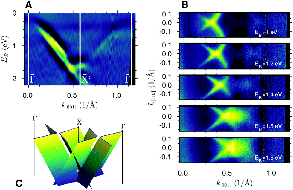 | ||
| Fig. 1 Electronic structure of Bi/Si(110) (photoemission intensity map) along the [001] direction (A) and the corresponding constant binding energy photoemission maps (B). (C) A sketch of the band structure of Bi/Si(110) around the point of the surface Brillouin zone. | ||
All the bands together with the corresponding ones located on the other side of the symmetry point merge at the point making a contact point located about 2 eV below the Fermi level. A sketch of the resulting electronic structure based on the series of experimentally derived constant energy cuts (Fig. S1, ESI†) is shown in Fig. 1C. It presents planes (i) which touch each other forming sharp edges and (ii) visible as linear bands in the E(k) and constant energy plots. Both features, the planes and the sharp edges in the k-space, are the most distinctive of the fortune teller-like states.
It is important to note that the electronic structure of bulk Si in the considered region of the Brillouin zone looks quite different compared to the results presented in this letter. According to the results of our calculations and the results of experimental and theoretical reports available in the literature11,12 there is only one bulk band approaching the point at the considered binding energy range, Fig. 2A (pink, solid line). In addition, that band is not linear in the close vicinity of the point of the Brillouin zone contrary to the bands obtained in the experiments reported here. Thus, the conclusion is that the observed bands certainly do not belong to the bulk Si crystal. Taking into account that ARPES is a surface sensitive technique – the outgoing photoelectrons come from at most several topmost layers – the observed bands can be assigned either to the Bi atoms sitting on the surface or to the Si surface layer. The former case can be excluded for several reasons. Firstly, it is tempting to assign the observed pair of bands to the Bi-induced lifting of the spin degeneracy of the surface states as often observed in silicon surfaces covered with Bi atoms.13,14 However, the Rashba-type splitting of the bands has been excluded – no spin polarization in the spin-resolved ARPES experiments is observed, Fig. S2 (ESI†). Secondly, as discussed below similar bands are also observed for the Si(110)–Pb and bare Si(110) surfaces, Fig. S3 (ESI†).
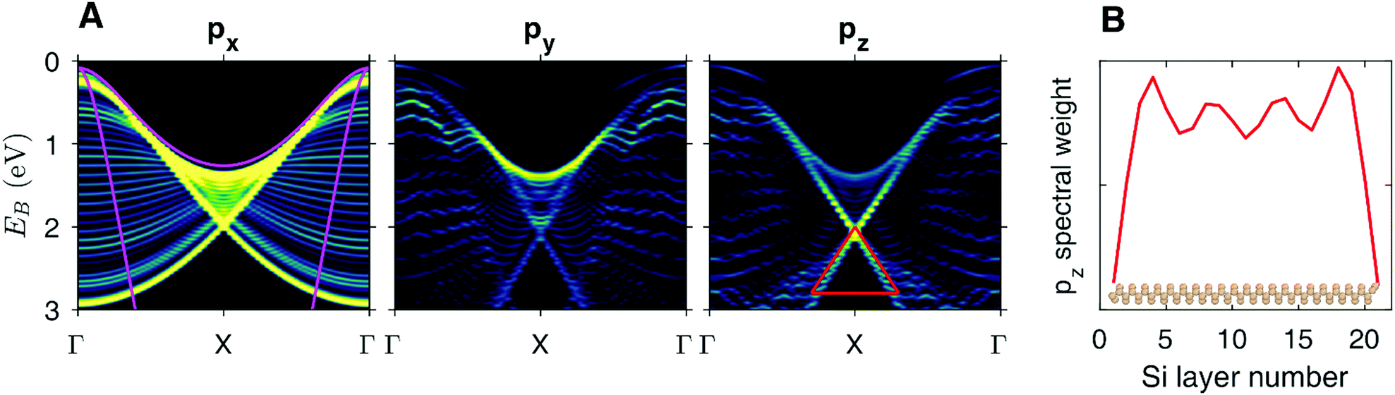 | ||
| Fig. 2 Electronic structure of Si(110) along the [001] direction – DFT results. (A) Relative contribution of the components of the p orbitals to the bands for the 4th Si layer presented as intensity maps. The pink, solid line in the px map presents bulk band structure. (B) Contribution of the pz component of the 3p orbitals to the bands in the region outlined by the red triangle in the pz map. | ||
Moreover, our DFT calculations10,15–19 indicate that the Bi atoms introduce non-dispersive, flat bands. On the other hand, the results of DFT calculations obtained for ultrathin layers of silicon of various thicknesses confirm the experimental findings and reveal linear bands around the point of the Brillouin zone, Fig. 2A. In addition, the calculations indicate that the spectral weight of the considered bands exhibits oscillations across the slab and is clearly enhanced at both its interfaces, Fig. 2B. The observed oscillations are the result of the interference effects between incoming and reflected at the surface wave functions. In a real system, we expect damping of theses oscillations towards the bulk. Nevertheless, the interference-induced states persist just below the surface. Thus this region can be regarded as a (quasi) 2D system.
Fig. 2A presents the relative contribution of the 3p orbitals of Si (plotted as intensity maps) to the electronic bands around the point. The contribution of other orbitals to the considered bands is negligible. It is clear that the main contribution to the linear bands comes from the px and pz components. It is interesting to note that the px orbitals do not contribute to the linear bands below the contact point. Those bands are mostly defined by the pz component and weak component of py (z axis is perpendicular to the surface, parallel to [110], y axis is parallel to [001]). This indicates that the pz component and therefore the linear bands below the contact point are associated with the bonds between the atoms lying in the neighbouring (110) planes within the considered 2D layer. It also means that in the bulk where there is no distinguished 2D layer, such electronic states cannot exist. On the other hand, above the contact point there is a bulk band which is formed by all three components of the p orbitals.
As suggested by the authors of ref. 9 adding dopants/other elements to the target system without changing its symmetry does not affect the FT dispersion. This is exactly what is observed in the ARPES experiments: the addition of Bi or Pb does not influence the FT states. The preparation of (3 × 2) (with only 0.1 ML Bi) or (1 × 1) (with 1 ML Bi or 1 ML Pb) surface reconstructions does not influence the existence and the shape of the bands. It only changes the position of the contact point at the X point, Fig. S3 (ESI†), or adds/removes other surface state bands. Similarly, the bare Si(110) surface which reveals (16 × 2) reconstruction also hosts the FT states. The FT bands in this case are considerably weaker compared to those obtained for the (1 × 1) Bi or Pb-reconstructed surface. Apparently, it is caused by the existence of different surface reconstructions: (1 × 1) in the case of adsorption of 1 ML Bi or Pb and (16 × 2) formed on the bare surface which very likely obscures the considered bands.
The energy position of the contact point with respect to the Fermi level depends on a particular system and on band filling. In the studied system the contact point is located about 2 eV below the Fermi level allowing observation of linearity of the bands above that point. In the cases of the (1 × 1)-Pb and the bare (16 × 2) surfaces the contact point is located at 1.6 and 2.0 eV below the Fermi level, respectively. The free layer of Si with the required symmetry has lattice constants of 3.74 Å and 4.64 Å.9 For such layers the contact point is located 2.30 eV below EF. In our case the lattice constants are different, 5.43 Å and 3.84 Å, and the surface layer is directly connected to the rest of the crystal; thus we do not expect the same position of the contact point as in ref. 9 although both values are very close.
Interestingly, there is a gap between the linear bands as seen in Fig. 1A and in more detail in Fig. S4 (ESI†). According to the authors of ref. 9 the appearance of the gap might be caused by a contact between one face of the sample and a substrate. Such contact reduces the symmetry of the system and opens a gap. The same effect can be obtained when an electric field is applied perpendicularly to the sample. In fact, both cases occur in the investigated system: the surface region responsible for the existence of linear bands is directly connected to the bulk as a part of the Si sample and the surface region experiences strong band bending resulting in an electric field perpendicular to the surface. The opening of the energy gap clearly points to a possibility of tailoring the electronic properties in such systems.
Conclusions
In conclusion, we have experimentally demonstrated the existence of a new type of massless fermion in quasi 2D crystals. It appears that the surface region of the (110) face of silicon possesses singular electronic structure consisting fortune teller-like states. This discovery paves a route for searching for other materials revealing such extraordinary electronic properties and designing new devices utilizing strongly anisotropic ultrafast charge carriers.Conflicts of interest
The authors declare no competing interests.Acknowledgements
This work was supported by the National Science Centre Poland under Grant No. 2013/11/B/ST3/04003.References
- L. A. Ponomarenko, R. V. Gorbachev, G. L. Yu, D. C. Elias, R. Jalil, A. A. Patel, A. Mishchenko, A. S. Mayorov, C. R. Woods, J. R. Wallbank, M. Mucha-Kruczynski, B. A. Piot, M. Potemski, I. V. Grigorieva, K. S. Novoselov, F. Guinea, V. I. Fal’ko and A. K. Geim, Cloning of Dirac fermions in graphene superlattices, Nature, 2013, 497, 594–597 CrossRef CAS PubMed.
- B. J. Wieder, Y. Kim, A. M. Rappe and C. L. Kane, Double Dirac semimetals in three dimensions, Phys. Rev. Lett., 2016, 116, 186402 CrossRef PubMed.
- P. Tang, Q. Zhou, G. Xu and S.-C. Zhang, Dirac fermions in an antiferromagnetic semimetal, Nat. Phys., 2016, 12, 1100–1104 Search PubMed.
- Z. Wang, A. Alexandradinata, R. J. Cava and B. Bernevig, Hourglass fermions, Nature, 2016, 532, 189–194 CrossRef CAS PubMed.
- J. Ma, C. Yi, B. Lv, Z. Wang, S. Nie, L. Wang, L. Kong, Y. Huang, P. Richard, P. Zhang, K. Yaji, K. Kuroda, S. Shin, H. Weng, B. A. Bernevig, Y. Shi, T. Qian and H. Ding, Experimental evidence of hourglass fermion in the candidate nonsymmorphic topological insulator KHgSb, Sci. Adv., 2017, 3, e1602415 CrossRef PubMed.
- P. Tang, Q. Zhou and S.-C. Zhang, Multiple types of topological fermions in transition metal silicides, Phys. Rev. Lett., 2017, 119, 206402 CrossRef PubMed.
- Z. K. Liu, B. Zhou, Y. Zhang, Z. J. Wang, H. M. Weng, D. Prabhakaran, S.-K. Mo, Z. X. Shen, Z. Fang, X. Dai, Z. Hussain and Y. L. Chen, Discovery of a three-dimensional topological Dirac semimetal, Na3Bi, Science, 2014, 343, 864–867 CrossRef CAS PubMed.
- B.-J. Yang and N. Nagaosa, Classification of stable three-dimensional Dirac semimetals with nontrivial topology, Nat. Commun., 2014, 5, 4898 CrossRef CAS PubMed.
- V. Damljanović, I. Popov and R. Gajić, Fortune teller fermions in two-dimensional materials, Nanoscale, 2017, 9, 19337–19345 RSC.
- ESI†.
- N. D. Kim, Y. K. Kim, C.-Y. Park, H. W. Yeom, H. Koh, E. Rotenberg and J. R. Ahn, High-resolution photoemission spectroscopy study of the single-domain Si(110)-16 × 2 surface, Phys. Rev. B: Condens. Matter Mater. Phys., 2007, 75, 125309 CrossRef.
- K. Sakamoto, M. Setvin, K. Mawatari, P. E. J. Eriksson, K. Miki and R. I. G. Uhrberg, Electronic structure of the Si(110)-(16 × 2) surface: High-resolution ARPES and STM investigation, Phys. Rev. B: Condens. Matter Mater. Phys., 2009, 79, 045304 CrossRef.
- I. Gierz, T. Suzuki, E. Frantzeskakis, S. Pons, S. Ostanin, A. Ernst, J. Henk, M. Grioni, K. Kern and C. R. Ast, Silicon surface with giant spin splitting, Phys. Rev. Lett., 2009, 103, 046803 CrossRef CAS PubMed.
- K. Sakamoto, H. Kakuta, K. Sugawara, K. Miyamoto, A. Kimura, T. Kuzumaki, N. Ueno, E. Annese, J. Fujii, A. Kodama, T. Shishidou, H. Namatame, M. Taniguchi, T. Sato, T. Takahashi and T. Oguchi, Peculiar Rashba splitting originating from the two-dimensional symmetry of the surface, Phys. Rev. Lett., 2009, 103, 156801 CrossRef PubMed.
- P. E. Blöchl, Projector augmented-wave method, Phys. Rev. B: Condens. Matter Mater. Phys., 1994, 50, 17953–17979 CrossRef PubMed.
- J. P. Perdew, K. Burke and M. Ernzerhof, Generalize gradient approximation made simple, Phys. Rev. Lett., 1996, 77, 3865–3868 CrossRef CAS PubMed.
- G. Kresse and J. Furthmüller, Efficient iterative schemes for ab initio total-energy calculations using a plane-wave basis set, Phys. Rev. B: Condens. Matter Mater. Phys., 1996, 54, 11169–11186 CrossRef CAS PubMed.
- G. Kresse and D. Joubert, From ultrasoft pseudopotentials to the projector augmented-wave method, Phys. Rev. B: Condens. Matter Mater. Phys., 1999, 59, 1758–1775 CrossRef CAS.
- H. J. Monkhorst and J. D. Pack, Special points for Brillouin-zone integrations, Phys. Rev. B: Condens. Matter Mater. Phys., 1976, 13, 5188–5192 CrossRef.
Footnote |
| † Electronic supplementary information (ESI) available. See DOI: 10.1039/c9nh00681h |
| This journal is © The Royal Society of Chemistry 2020 |