
Direct electroplating of Ag nanowires using superionic conductors†
Zeliang
Guo
 ,
Yusen
Zhao
,
Shipeng
Sun
and
Hui
Wu
*
,
Yusen
Zhao
,
Shipeng
Sun
and
Hui
Wu
*
State Key Lab of New Ceramics and Fine Processing, School of Materials Science and Engineering, Tsinghua University, Beijing 100084, China. E-mail: huiwu@tsinghua.edu.cn
First published on 26th July 2019
Abstract
Solid electrolytes can be applied in the metal electrodeposition industry. We propose a new strategy for fabricating Ag and Cu nanowire arrays by direct all-solid electroplating. The Ag nanowires are uniformly aligned and have a controllable length ranging between 2 μm and 300 μm. Moreover, the Ag nanowires show uniform lattice orientation on a large scale. By designing and altering the pattern of the electrolyte surface, the plated layer shows the corresponding patterns. This new electroplating strategy provides new insights to metal nanowire growth and patterned coating designs that are simple, inexpensive and versatile.
New conceptsAs solid electrolytes have poor electrode wettability compared to liquid electrolytes, they have not been used in electroplating for material production. However, if we consider exploiting the non-wetting contact property of solid–solid interfaces, metal materials can grow in a completely different way compared to their growth in liquid electrolytes. In this research, we successfully fabricated close-packed Ag nanowires having a uniform alignment and controllable length ranging between 2 μm and 300 μm by direct all-solid electroplating utilizing the superionic conductors RbAg4I5 and RbCu4Cl2I3 as electrolytes. Thus, we achieved a new mask-free and template-free method for selected area electroplating. By designing and altering the pattern of the electrolyte surface, the plated layer shows the corresponding micrometer-scale patterns. |
Introduction
Metal electrodeposition technology is widely applied in the material manufacturing industry, including surface decorating, protective coating, and conductive coating. It is also widely used in advanced applications such as in microelectronic device manufacturing,1 energy conversion device manufacturing2–6 and biomaterial surface coating.7 Moreover, research efforts to advance the application of electrodeposition technology for creating different materials are still ongoing.8,9 For electrolytes, a rich variety of electrolyte systems, including aqueous solutions, organic liquid solutions and molten salt systems, have been explored. However, solid electrolytes have not been used in electroplating for material production because they have poor electrode wettability compared to liquid electrolytes. Another field of research concern is selected area electroplating. To create specific patterns on material surfaces, stereolithography is commonly used to create masks for subsequent electroplating.10,11 Local electroplating using scanning probes has been reported since 1988.12–14 Although patterns with high resolution have been created, it is difficult to achieve their mass production and macroscopic sizes. A straightforward mask-free process can eliminate the cost and labor used in selected area electroplating. However, if we consider exploiting the non-wetting surface contact property of solid electrolytes, metal materials can grow in a completely different way compared to their growth in liquid electrolytes. We can also achieve a new mask-free method for selected area electroplating. Metal nanowires exhibit outstanding physical and chemical properties because of which they have been widely applied as flexible conductors,15–18 catalysts,19,20 sensors,21,22 and optoelectronic devices.23,24 The fabrication methods of Ag nanowires include solution processing,16,24,25 metal deposition26,27 and spinning.28,29 In these methods, high temperature, high voltage or complicated devices are used. Moreover, to obtain nanowires with uniform alignment, the usage of templates such as AAO and single crystal substrates is inevitable. Industrial application of metal nanowires needs to be further increased using a novel method that is both versatile and inexpensive.In this study, we propose a new strategy for fabricating Ag and Cu nanowire arrays by direct all-solid electroplating utilizing superionic conductors RbAg4I5 and RbCu4Cl2I3 as electrolytes. We successfully fabricated close-packed Ag nanowires that are uniformly aligned with a controllable length ranging between 2 μm and 300 μm. The widths of Ag nanowires were between 100 and 300 nm. Moreover, the Ag nanowires grown in this way show uniformed lattice orientation on a large scale along the nanowire growth direction. Furthermore, the Ag nanowire arrays are closely packed into a free-standing foil whose thickness equals to the length of the nanowires. The same mechanism also works for the all-solid electroplating of Cu. By designing and altering the pattern of the electrolyte surface, the plated layer shows the corresponding patterns. More importantly, electrodeposition in liquid solutions usually produces waste water containing hazardous contents,30,31 which leads to the problem of waste removal. The new electroplating strategy provides new insights into metal nanowire growth and a patterned coating design that is simple, inexpensive and versatile.
Experimental
Electrolyte preparation
All materials used were of high purity. RbAg4I5 was prepared by melting RbI (Sigma-Aldrich, 99.9%) and AgI (Shanghai Xianding Biotechnology Co., Ltd, 99%) in a molar ratio of 1![[thin space (1/6-em)]](https://www.rsc.org/images/entities/char_2009.gif) :4 at 420 °C in an argon-filled glovebox. 3 g of the molten mixture was quenched in a marble container at room temperature. Then, the solid product was ground and annealed at 190 °C for 10 h. The annealed material was ground using a marble mortar. 0.9 g of the powder was added to a stainless steel mould (12 mm radius) and pressed tight at 5.6 kN to form a compact tablet (thickness = ∼1.5 mm). RbCu4I3Cl2 was prepared by melting RbCl (Acros organics, 99.8%), CuCl (Alfa Aesar, 99%) and CuI (Shanghai Hushi Laboratorial Equipment Co., Ltd, 99.5%) in a molar ratio of 1:1:3 at 500 °C in an argon-filled glovebox. Then, the solid product was ground and annealed at 200 °C for 10 h. The reshaping process of RbCu4I3Cl2 is the same as that of RbAg4I5.
:4 at 420 °C in an argon-filled glovebox. 3 g of the molten mixture was quenched in a marble container at room temperature. Then, the solid product was ground and annealed at 190 °C for 10 h. The annealed material was ground using a marble mortar. 0.9 g of the powder was added to a stainless steel mould (12 mm radius) and pressed tight at 5.6 kN to form a compact tablet (thickness = ∼1.5 mm). RbCu4I3Cl2 was prepared by melting RbCl (Acros organics, 99.8%), CuCl (Alfa Aesar, 99%) and CuI (Shanghai Hushi Laboratorial Equipment Co., Ltd, 99.5%) in a molar ratio of 1:1:3 at 500 °C in an argon-filled glovebox. Then, the solid product was ground and annealed at 200 °C for 10 h. The reshaping process of RbCu4I3Cl2 is the same as that of RbAg4I5.
Cell assembly and electroplating
RbAg4I5 and RbCu4I3Cl2 electrolytes were placed in polytetrafluoroethylene (PTFE) rings to fix them from crushing. A silver foil (radius = 12 mm, thickness = 0.2 mm) and a stainless steel foil (radius = 12 mm, thickness = 0.1 mm) were placed at either sides of the electrode. The whole cell was insulated and clamped in a hot-press machine at 85 °C and 5 kN. The electrodeposition process was conducted on a CHI660e electrochemical workstation (Shanghai Chenhua Instruments). The stainless steel foil and silver foil were connected to the working electrode and counter electrode, respectively. A constant voltage was applied on the cell using the amperometric I–t curve method. During the electroplating process, the potential was set at −0.05 V for 10000 s and changed to 0.05 V for 1000 s during the reverse plating process. The all-solid electroplated layer was detached from the cell and washed in ethanol using an ultrasound cleaning machine for 60 s and then dried in air.
Characterization of nanostructured plate layer
All-solid electroplated Ag and Cu layers were characterized by scanning electron microscopy (Carl Ziess, Gemini 2), EDS (X-Max, Oxford instruments), transmission electron microscopy (jeol-ARM-200F, operated at 200 kV), and XRD (Rigaku D-Max-2500).Pattern transferring
The original honeycomb-like pattern was obtained on a stainless steel plate mould etched using a picosecond laser. The pattern was transferred onto the electrode during the tableting process, which created peaks and valleys on the electrode surface. During the electroplating process, the patterned surface of the electrode was connected to the stainless steel foil electrode. The patterned plate layer was detached from the cell and characterized using SEM.Results and discussion
The length of the obtained nanowires can be controlled between 2 and 300 μm, while the widths of Ag nanowires were between 100 and 300 nm. The nanowires were closely packed to form a freestanding thin foil. The fabrication process was both solvent-free and template-free. More importantly, the Ag nanowires are close-packed, self-standing and can be designed to form specific patterns. A similar all-solid electroplating method can be successfully applied to Cu and other metals too.The process of all-solid electrodeposition and fabricating silver nanowires starts with synthesizing the superionic conductor RbAg4I5. RbAg4I5, a kind of superionic conductor, was chosen as the electrolyte because of its high ionic conductivity at room temperature32 (σi = 0.32 S cm−1). RbAg4I5 was obtained by melt-quenching of RbI and AgI, and the product was then reshaped into tablets, as shown in Fig. 1a. In the second step, the RbAg4I5 pellet (diameter = 12 mm, thickness = 1.5 mm), a silver film anode and a stainless steel (SS) film cathode were assembled into a Ag(+)|RbAg4I5|SS(−) cell, and compressed under 50 MPa to ensure a good electronic contact between the electrode and electrolyte. The whole device was heated to 85 °C to enhance the ionic conductivity of the RbAg4I5 electrolyte, and thus speed up the electrodeposition process. We applied a DC voltage of −0.05 V on the cell. During the electrodeposition process, the current–time curve was recorded and shown in Fig. S1 (ESI†). As the electroplated layer fills the gap between the negative electrode and the electrolyte, the electric contact improves and the current goes up from 4 mA to 18 mA. After the total charge reached the target value, the electrodeposition process was stopped and a DC voltage of 0.05 V was applied on the cell. Since the interface bonding between the electroplated layer and the electrolyte is robust, such “reverse electroplating” process shown in Fig. 1b aims to remove a small amount of silver at the electrolyte-deposited layer interface, making it easy detach the deposited layer from the electrolyte. For the all-solid electrodeposition of Cu, we used RbCu4I3Cl2 as the electrode and applied the same electroplating method.
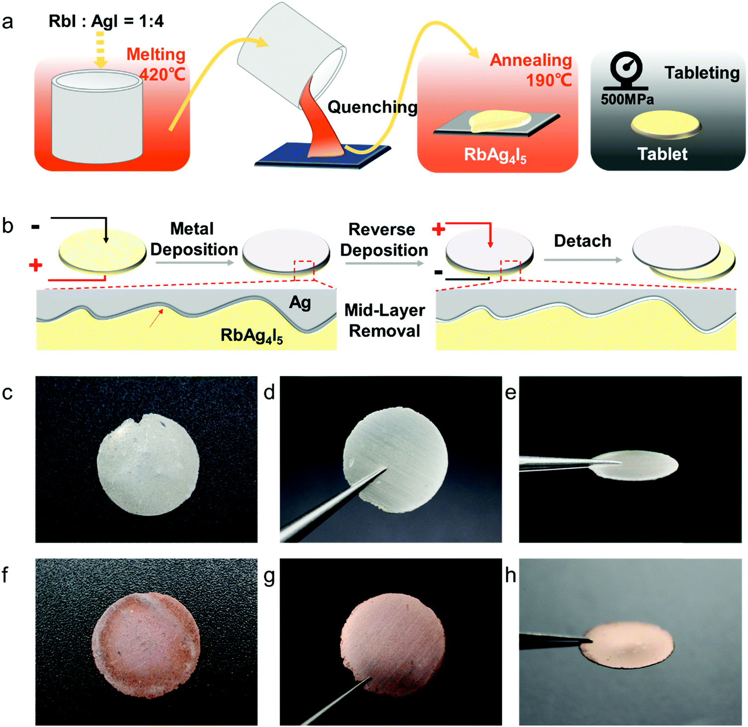 | ||
| Fig. 1 Self-standing all-solid electroplated Ag and Cu foils. Electrolyte preparation process (a) and electroplating process (b) are illustrated in diagrammatic sketches. (c–e) Ag foil fabricated by direct electroplating utilizing superionic conductor RbAg4I5 as electrolyte. (f–h) Cu foil fabricated by direct electroplating utilizing superionic conductor RbCu4I3Cl2 as electrolyte. Pictures show the surface (c and f), polished surface (d and g) and side view (e and h) of the Ag and Cu foil. | ||
The electrodeposited layer was peeled off from the electrolyte. Fig. 1c and f and Fig. S2 (ESI†) show the optical images of the original Ag and Cu layer, respectively. The whole layer remains intact and is freestanding without breaking or cracking (the Cu layer was slightly oxidized because the plating temperature was 85 °C). The XRD results of the deposited layers in Fig. S3 (ESI†) exhibit strong Ag and Cu peaks with no signal from any impurity. EDS analysis of the electroplated Ag layer surface shows that the electrodeposition layer consists of pure Ag element (Fig. S4, ESI†). Fig. S5 (ESI†) shows that the surface of the original Ag and Cu layer is clean and smooth under a scanning electron microscope (SEM). After being polished with a 3000 mesh sandpaper, the surface of the Ag and Cu layer still remained flawless without a hollow area or crack (Fig. 1d and e), which confirms that the electrodeposited layers are compact. Cross-sectional SEM images of the electrodeposited Ag layer in Fig. 2c–g show that the whole layered structure is constructed by a large number of close-packed nanowires. The nanowires are mutually parallel and have a uniform width and length. The length of the nanowire arrays can be controlled by setting the total charge to be transferred during the electrodeposition process. Fig. 2c–g also show the SEM images of the Ag electrodeposited layer at different charge densities: 2 C cm−2, 5 C cm−2, 10 C cm−2 and 150 C cm−2. During the process, the growth direction of the Ag nanowires remains vertical to the substrate. The isolated nanowires from the Ag electroplating layer are observed using transmission electron microscopy (TEM). The selected area diffraction patterns of a single Ag nanowire are shown in Fig. 3b–d. TEM images of nanowire margins on different sections of a single silver nanowire are shown in Fig. S7 (ESI†). The diffraction pattern at different positions along the nanowire show the same crystal orientation on a large scale along the nanowire growth direction, which is perpendicular to the crystal face (![[1 with combining macron]](https://www.rsc.org/images/entities/char_0031_0304.gif) 1) of Ag.
1) of Ag.
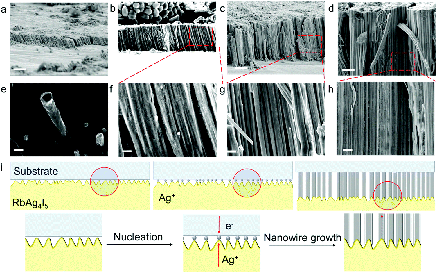 | ||
| Fig. 2 Growth track of all-solid electroplated Ag nanostructures SEM images of all-solid electroplated Ag with different deposition quantities. (a) and (e) 2 C cm−1; (b) and (f) 5 C cm−1; (c) and (g) 10 C cm−1; (d) and (h) 150 C cm−1. Scale bar, 5 μm (a)–(d); 300 nm (e); 1 μm (f)–(h). (i) Diagrammatic sketches illustrating the mechanism of all-solid electroplating. The nucleation and nanowire growth processes are focused at the hot spots. | ||
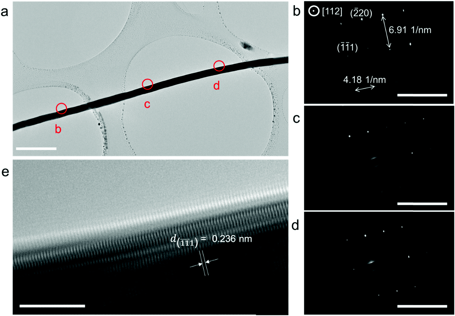 | ||
| Fig. 3 TEM images and diffraction patterns of Ag nanowire showing uniform lattice orientation on a large scale along the nanowire growth direction. (a) TEM picture of a separated silver nanowire. (b–d) TEM diffraction patterns of selected area on the nanowire. (e) Magnified TEM picture showing crystal planes vertical to the nanowire axial direction. Scale bar, 1 μm (a); 10 nm−1 (b)–(d); 5 nm (e). | ||
Structural properties of the all-solid electrodeposited layer obtained by our method significantly differ from those of the electrodeposited layer obtained in liquid electrolyte systems. Liquid electrolyte systems usually produce metal layers with equiaxed grains or dendrites; however, our all-solid electroplating systems produce uniform nanowires. This can be attributed to different reaction mechanisms in the liquid system and the solid system. In liquid systems, the electrolyte covers the entire surface of the electrode; thus, metal deposition reaction simultaneously takes place on the whole surface. However, in solid systems, poor solid–solid contact between the electrolyte and electrodes is a common problem.33,34 As shown in Fig. 2i, the electrolyte and the electrode contact at discrete spots, and metal deposition is focused at these “hot spots” (Fig. S9, ESI†). No deposition reaction takes place on other interface areas with no electrode–electrolyte contact. As the deposition process continues, fresh nucleation of Ag is observed at the “hot-spots”, connecting to the bottom of the previously deposited materials and pushing up the interface when they grow.35 Thus, all-solid electrodeposition produces Ag nanowire arrays. A similar phenomenon is also found in the all-solid electrodeposition of Cu. If properly protected, there is a great possibility that lithium and sodium nanowires can be produced using inorganic solid electrolytes and polymer electrolytes. Moreover, gel electrolytes, as well as the newly proposed “ice electrolytes”36 provide the possiblity for a wide range of other metals such as Zn, Ni and Fe to be all-solid electroplated.
In aqueous electroplating systems, electrodes are immersed in the liquid electrolyte; thus, the electrodeposited layer are usually uniformly grown. However, in all-solid electroplating systems, gaps exist at the interface. The contact region between the electrolyte and electrode can be altered by changing the surface pattern of the electrolyte, and then the electrodeposited layer can be designed to form specific patterns. We used a honeycomb-like hexagonal template to illustrate this idea. Superionic RbAg4I5 pellets were reshaped under pressure using a stainless steel mould. Then, a flat stainless steel substrate was stuck to the reshaped side of the RbAg4I5 pellet (cathode side) and a Ag foil was stuck to the other side (anode side). The voltage of the electrodeposition process was set to −0.05 V. SEM images of the obtained electrodeposited layer in Fig. 4a and b shows that the honeycomb-like pattern of the mould is successfully replicated on the electrodeposited layer. The thickness of “walls” in the honeycomb-like pattern is 80 μm. After the electrodeposition process, the RbAg4I5 electrolyte can be pressed and reshaped again to reuse the material. XRD results in Fig. S8 (ESI†) prove that, after the electrodeposition process, the electrolyte remains in the original phase. The reusage of electrolyte reduces the waste of materials and eliminates hazardous by-products. At the stage of 100 nm feature size, all-solid electroplating patterning has the potential to be applied in micro pattern printing, optoelectronic devices and wearable electronic devices. Note that this method has not pushed the limit of fineness of the pattern. Optimizing this method can help to create more meticulous patterns.
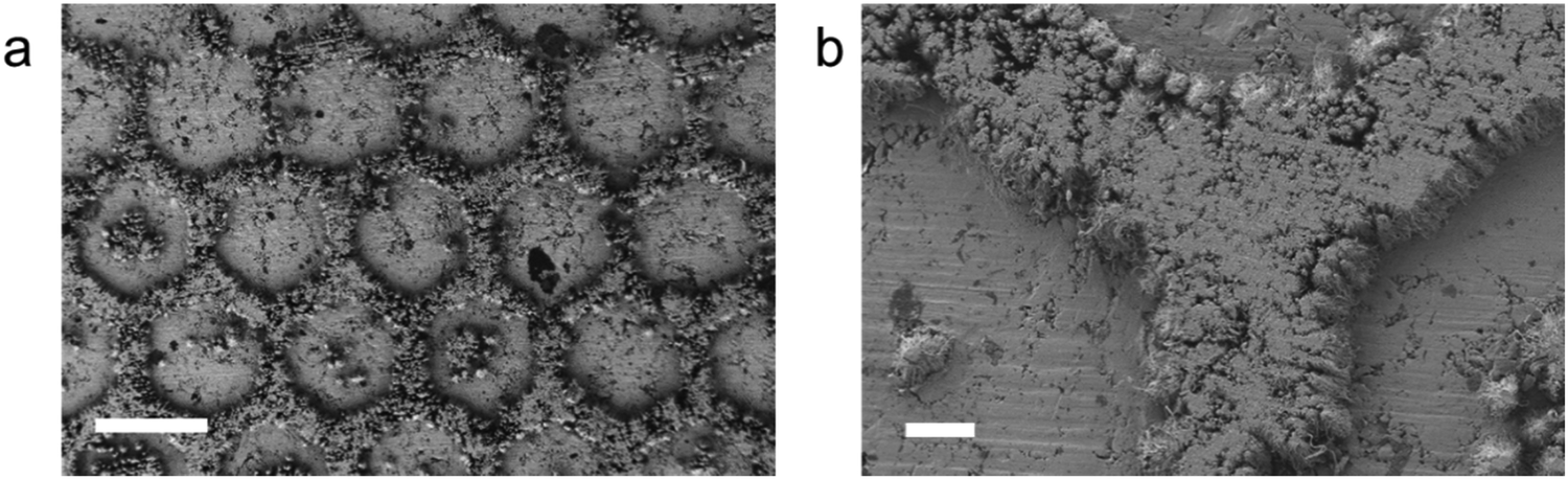 | ||
| Fig. 4 Patterns of electrodeposited Ag layer created by designing the surface of the electrolyte. (a) SEM picture showing the hexagonal pattern of Ag layer. (b) Zoom-in SEM picture showing details of the hexagonal pattern of Ag layer. Scale bar, 500 μm (a), 50 μm (b). | ||
Conclusions
In conclusion, we introduce a novel all-solid electrodeposition system using RbAg4I5 as an electrolyte. The same method can be applied to other electrolytes such as RbCu4I3Cl2. The electrodeposited layer is made up of pure Ag and consists of closely packed, mutually parallel and uniform Ag nanowire arrays. Moreover, the nanowires show same crystal orientation on a large scale. These properties can be explained by the specific “hot spot” model caused by the discrete contact between the solid electrolyte and the flat electrode. These unique properties can be widely utilized for producing metal nanowires and directly depositing metal layers with specific patterns. A new material growth mode in electrodeposition was provided by an all-solid electrodeposition technique, thus opening up new avenues in the field of electrodeposition, nanomaterial preparation and metal patterning.Conflicts of interest
There are no conflicts to declare.Acknowledgements
We are grateful for funding from the National Natural Science Foundation of China (51788104, 51661135025, 51706117 and U1564205) and the National Basic Research of China (2015CB932500, 2016YFE0102200 and 2018YFB0104404).Notes and references
- T. A. Green, Gold Bull., 2007, 40, 105 CrossRef CAS.
- Z. Liu, T. Cui, G. Pulletikurthi, A. Lahiri, T. Carstens, M. Olschewski and F. Endres, Angew. Chem., Int. Ed., 2016, 55, 2889–2893 CrossRef CAS PubMed.
- D. K. Zhong, M. Cornuz, K. Sivula, M. Grätzel and D. R. Gamelin, Energy Environ. Sci., 2011, 4, 1759 RSC.
- X. Xia, J. Tu, Y. Zhang, J. Chen, X. Wang, C. Gu, C. Guan, J. Luo and H. J. Fan, Chem. Mater., 2012, 24, 3793 CrossRef CAS.
- X. Lu and C. Zhao, Nat. Commun., 2015, 6, 6616 CrossRef CAS PubMed.
- Y. Lu, Z. Tu and L. A. Archer, Nat. Mater., 2014, 13, 961 CrossRef CAS.
- Y. W. Song, D. Y. Shan and E. H. Han, Mater. Lett., 2008, 62, 3276 CrossRef CAS.
- Q. Zhang, Q. Wang, S. Zhang, X. Lu and X. Zhang, Chem. Phys. Chem., 2016, 17, 335 CrossRef CAS.
- M. D. Tikekar, L. A. Archer and D. L. Koch, Sci. Adv., 2016, 2, e1600320 CrossRef.
- M. A. Zeeshan, R. Grisch, E. Pellicer, K. M. Sivaraman, K. E. Peyer, J. Sort, B. Özkale, M. S. Sakar, B. J. Nelson and S. Pané, Small, 2014, 10, 1284 CrossRef CAS.
- M. Miyake, Y. C. Chen, P. V. Braun and P. Wiltzius, Adv. Mater., 2009, 21, 3012 CrossRef CAS.
- D. H. Craston, W. L. Charles and A. J. Bard, J. Electrochem. Soc., 1988, 135, 785 CrossRef CAS.
- M. Sheffer and D. Mandler, J. Electrochem. Soc., 1995, 142, L82 CrossRef.
- L. Hirt, S. Ihle, Z. Pan, L. D. Carter, A. Reiser, J. M. Wheeler, R. Spolenak, J. Vörös and T. Zambelli, Adv. Mater., 2016, 28, 2311 CrossRef CAS.
- J. Lee, S. T. Connor, Y. Cui and P. Peumans, Nano Lett., 2008, 2, 689 CrossRef.
- H. Wu, D. Kong, Z. Ruan, P. C. Hsu, S. Wang, Z. Yu, T. J. Carney, L. Hu, S. Fan and Y. Cui, Nat. Nanotechnol., 2013, 8, 421 CrossRef CAS.
- C. F. Guo and Z. Ren, Mater. Today, 2015, 18, 143 CrossRef CAS.
- S. Yao and Y. Zhu, Adv. Mater., 2015, 27, 1480 CrossRef CAS.
- S. Guo, D. Li, H. Zhu, S. Zhang, N. M. Markovic, V. R. Stamenkovic and S. Sun, Angew. Chem., 2013, 125, 3549 CrossRef.
- C. Wang, Z. Zhang, G. Yang, Q. Chen, Y. Yin and M. Jin, Nano Lett., 2016, 9, 5669 CrossRef.
- K. K. Kim, S. Hong, H. M. Cho, J. Lee, Y. D. Suh, J. Ham and S. H. Ko, Nano Lett., 2015, 8, 5240 CrossRef.
- M. Amjadi, A. Pichitpajongkit, S. Le, S. Ryu and I. Park, ACS Nano, 2014, 8, 5154 CrossRef CAS.
- D. Lee, H. Lee, Y. Ahna, Y. Jeonga, D. Leeb and Y. Lee, Nanoscale, 2013, 17, 7750 RSC.
- H. Lee, M. Kim, I. Kim and H. Lee, Adv. Mater., 2016, 28, 4541 CrossRef CAS.
- B. Bari, J. Lee, T. Jang, P. Won, S. H. Ko, K. Alamgir, M. Arshad and L. J. Guo, J. Mater. Chem. A, 2016, 29, 11365 RSC.
- M. Song, D. S. You and K. Lim, Adv. Funct. Mater., 2013, 34, 4177 CrossRef.
- G. Y. Margulis, M. G. Christoforo, D. Lam, Z. M. Beiley, A. R. Bowring, C. D. Bailie, A. Salleo and M. D. McGehee, Adv. Energy Mater., 2013, 12, 1657 CrossRef.
- L. Hu, H. Wu and Y. Cui, MRS Bull., 2011, 36, 760 CrossRef CAS.
- S. Lin, H. Wang and F. Wu, npj. Flexible Electron., 2019, 3, 6 CrossRef.
- S. A. Cavaco, S. Fernandes, M. M. Quina and L. M. Ferreira, J. Hazard. Mater., 2007, 144, 634 CrossRef CAS.
- J. Liu, X. H. Zhang, H. Tran, D. Q. Wang and Y. N. Zhu, Environ. Sci. Pollut. Res., 2011, 18, 1623 CrossRef CAS.
- B. B. Owens and G. R. Argue, Science, 1967, 157, 308 CrossRef CAS.
- S. S. Chi, Y. Liu, N. Zhao, X. Guo, C. W. Nan and L. Z. Fan, Energy Storage Mater., 2019, 17, 309 CrossRef.
- C. Wang, Y. Gong, J. Dai, L. Zhang, H. Xie, G. Pastel, B. Liu, E. Wachsman, H. Wang and L. Hu, J. Am. Chem. Soc., 2017, 139, 14257 CrossRef CAS.
- W. M. Schuette and W. E. Buhro, ACS Nano, 2013, 7, 3844 CrossRef CAS PubMed.
- Z. Guo, et al. , Angew. Chem., Int. Ed., 2019 DOI:10.1002/anie.201907832.
Footnote |
| † Electronic supplementary information (ESI) available. See DOI: 10.1039/c9nh00395a |
| This journal is © The Royal Society of Chemistry 2020 |