DOI:
10.1039/C9NH00299E
(Communication)
Nanoscale Horiz., 2020,
5, 82-88
Superior phototransistors based on a single ZnO nanoparticle with high mobility and ultrafast response time†
Received
8th May 2019
, Accepted 7th August 2019
First published on 7th August 2019
Abstract
Conventional film-structured polycrystalline semiconductor devices suffer from grain boundary scattering, which is responsible for low mobility and can even mask intrinsic transport properties. In this work, we show that devices containing only a ZnO single particle can exhibit mobility values one order higher than that of single-crystal nanowires. The ZnO nanoparticle was embedded inside a nanopore structure, surrounded by a gate electrode and connected to top and bottom electrodes. Due to the absence of inter-grain scattering and long traveling distance, we obtained relatively high mobility values of around 600 cm2 V−1 s−1 at room temperature (300 K) and about 1100 cm2 V−1 s−1 at low temperature (∼180 K). The devices also presented external quantum efficiency of 5.6 × 10⁷, responsivity of 1.39 × 10⁶ AW−1, detectivity of 8.69 × 10¹² Jones, and a record-high photoresponse rise time of 90 μs. This single nanoparticle-based device could be an excellent candidate of phototransistors with high performances.
New concepts
In this work, the new concept is a single ZnO nanoparticle embedded inside the nanopore structure which exhibits relatively higher mobility and responsivity than that of devices made of polycrystal and single-crystal materials. The excellent physical properties are due to elimination of scattering from inter-grain boundaries and the absence of long traveling distance. The most important feature is a quick photoresponse rising time of 90 μs which is the record-high value in the state of the art.
|
Introduction
Zinc oxide (ZnO) has unique electric and opto-electric properties (including wide band gap (3.37 eV) and high exciton binding energy (60 meV)) and has emerged as a strong candidate for applications in electronics and optoelectronics.1–4 Particularly, ZnO-based field-effect-transistors (FETs) have been extensively explored and have exhibited high mobility, high on/off ratio, high transconductance gain, and low operating voltages.5–8 It is also found that devices containing ZnO nanostructures as an active conducting channel exhibit a variety of novel properties with enhancements in electrical performance due to quantum confinement.9–12 Electronic devices with a single ZnO nanoparticle may be of particular interest as they possess several advantages over 1D and 2D structures. An obvious advantage is the large surface-to-volume ratio, which promises high sensitivity with light illumination. Other advantages are absence of boundary scattering and short conducting channel, which can reduce the probability of inter-grain boundary scattering and thus improve carrier mobility and subsequently prolong the carrier lifetime.
To evaluate the intrinsic mobility of ZnO and to explore unique properties of single-ZnO-particle devices, we fabricated and studied devices containing an individual nanoparticle. The nanoparticle was surrounded by a gate electrode and sandwiched between top and bottom electrodes. Due to a strong capacitive coupling from the surrounded gate electrode, the transconductance reached around 2.6 μS. At room temperature, the devices exhibited n-type behavior with a high mobility value of around 600 cm2 V−1 s−1, while about 1100 cm2 V−1 s−1 was obtained at low temperature. With this high mobility the device showed an external quantum efficiency (EQE) value of 5.6 × 10⁷ with ultrafast response rise time of 90 μs upon 365 nm ultraviolet light emitting diode (UV-LED) illumination. Mechanisms governing photo-induced electron transport and high-performance behaviors with ultrafast response time were discussed.
Materials and methods
Material characteristics
Commercially available ZnO nanoparticles (purity 99.99%) with diameters ranging from 50 nm to 100 nm were used here. Fig. 1a and Fig. S1 (ESI†) show a high-resolution transmission electron microscopy (HRTEM) image of the single ZnO nanoparticle, which reveals periodic atom arrangement. No obvious crystalline defects in the ZnO nanoparticle are found in the HRTEM image, indicating a high quality of crystalline structure. The clear lattice fringes with d spacing of 0.52 nm and 0.28 nm can be observed, corresponding to (0001) and (10![[1 with combining macron]](https://www.rsc.org/images/entities/char_0031_0304.gif) 0) lattice planes of hexagonal wurtzite ZnO, respectively.13Fig. 1b displays the selected area electron diffraction (SAED) pattern with sharp and clear diffraction spots, which again confirms a highly crystalline nature of the ZnO nanoparticle. It is also noted from TEM-based energy dispersive spectroscopy (TEM-EDS) analysis (Fig. 1c) that the atomic percentage ratio between Zn and O is 1
0) lattice planes of hexagonal wurtzite ZnO, respectively.13Fig. 1b displays the selected area electron diffraction (SAED) pattern with sharp and clear diffraction spots, which again confirms a highly crystalline nature of the ZnO nanoparticle. It is also noted from TEM-based energy dispersive spectroscopy (TEM-EDS) analysis (Fig. 1c) that the atomic percentage ratio between Zn and O is 1![[thin space (1/6-em)]](https://www.rsc.org/images/entities/char_2009.gif) :1, indicating the high purity of the ZnO nanoparticle. Fig. 1d shows the optical absorption and photoluminescence (PL) spectra of ZnO nanoparticles at room temperature. It is found that ZnO nanoparticles exhibit a strong excitonic absorption at 372 nm and a band edge emission peak at 383 nm, which is slightly blue-shifted with respect to the bulk ZnO.14,15 It is also noted from the PL spectrum that the emission peak recorded at 383 nm indicates strong absorption of nanoparticles under photo-excitation with a 365 nm UV light source. With this excitation, it is still distinguishable to recognize two peaks with the separation around 18 nm (resolution for the spectrum is 0.3 nm) and it also has enough energy (3.4 eV) to excite the photocurrent (band gap is 3.24 eV) in this experiment. In addition, we notice that a broad spectrum appears in the optical absorption as shown in Fig. 1d. From the theoretical prediction on the absorbance as a function of wavelength with different size of nanoparticles, the larger the size the wider an absorption spectrum should be observed.16 Based on this theory, our nanoparticle with size around 80 nm is reasonable to observe a broad absorption spectrum17 in our experiment.
:1, indicating the high purity of the ZnO nanoparticle. Fig. 1d shows the optical absorption and photoluminescence (PL) spectra of ZnO nanoparticles at room temperature. It is found that ZnO nanoparticles exhibit a strong excitonic absorption at 372 nm and a band edge emission peak at 383 nm, which is slightly blue-shifted with respect to the bulk ZnO.14,15 It is also noted from the PL spectrum that the emission peak recorded at 383 nm indicates strong absorption of nanoparticles under photo-excitation with a 365 nm UV light source. With this excitation, it is still distinguishable to recognize two peaks with the separation around 18 nm (resolution for the spectrum is 0.3 nm) and it also has enough energy (3.4 eV) to excite the photocurrent (band gap is 3.24 eV) in this experiment. In addition, we notice that a broad spectrum appears in the optical absorption as shown in Fig. 1d. From the theoretical prediction on the absorbance as a function of wavelength with different size of nanoparticles, the larger the size the wider an absorption spectrum should be observed.16 Based on this theory, our nanoparticle with size around 80 nm is reasonable to observe a broad absorption spectrum17 in our experiment.
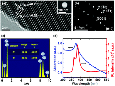 |
| | Fig. 1 Characterization of ZnO nanoparticles. (a) High-resolution TEM image. The inset shows the SEM image of a single ZnO nanoparticle. (b) The SAED pattern taken along the [010] zone axis. (c) TEM-EDS analysis of the composition ratio. (d) Optical absorption (blue curve) and photoluminescence (red curve) spectra of the ZnO nanoparticles recorded at room temperature. | |
Experimental section
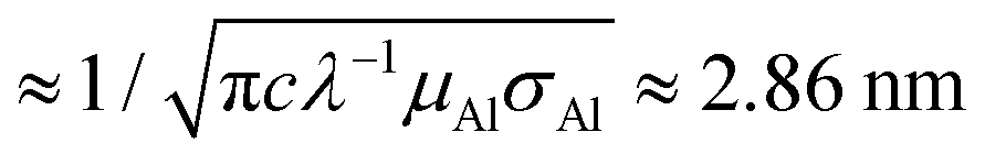
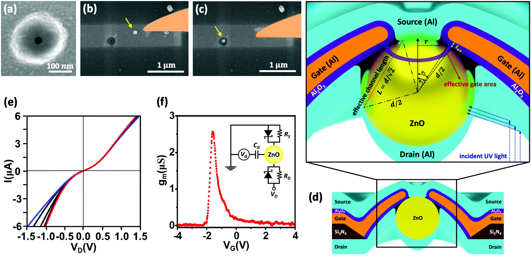
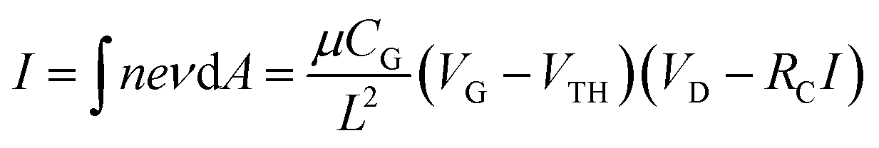
The device structure and fabrication process are illustrated in Fig. 2. Firstly, e-beam lithography and reactive-ion etching were applied to create a bowl-shape hole on the silicon nitride (Si3N4) membrane. This was followed by another e-beam lithography and e-gun deposition of a 400 nm-wide and 24 nm-thick aluminum (Al) strip; an 8 nm-thick aluminum oxide (Al2O3) layer was grown by oxidization. The Al strip serves as a gate and the Al2O3 layer is to isolate the gate electrode from the source and drain electrodes, which are to be made at a later stage. The Al/Al2O3 layer formed a volcano-shape nanopore structure on the membrane with the diameter of the crater about 30 nm as shown in Fig. 2a. ZnO nanoparticles were then dispersed onto the backside of the membrane around the nanopore and a selected single ZnO nanoparticle was manipulated and placed into the bottom side of the nanopore by using a nano-manipulator (Zyvex S100) installed inside the field-emission scanning electron microscope (FEI Sirion 600) chamber; the manipulation process is shown in Fig. 2b and c. Optical fiber tips of diameters as small as 50 nm were employed to manipulate the ZnO nanoparticle. Details of nanopore fabrication and single nanoparticle manipulation procedures can be found in ref. 18. After placing the ZnO nanoparticle, around 30 nm-thick Al films were thermally-evaporated onto the top and bottom sides to form source and drain electrodes, respectively. Fig. 2d schematically illustrates the cross-section of a completed device structure. In order to explain the reason why UV light can penetrate through metal, we illustrate the potential situation for our case below. The thickness of the drain electrode at the side wall of the nanoparticle must be much thinner than that on the top due to an anisotropic metal deposition process. The penetration depth δ of aluminum is  , where c is the speed of light and λ is the wavelength of the incident light; μAl and σAl are permeability and conductivity of aluminum, respectively.19 According to the schematic geometry in Fig. 2d, the drain electrode on the side wall of the nanoparticle could be below 2.86 nm while 30 nm thick metal was perpendicularly deposited on the top. Therefore, the UV light is able to penetrate through the metal and interact with the ZnO nanoparticle. All the electrical measurements were performed in a Physical Property Measurement System (PPMS from Quantum Design) with a homemade current–voltage amplifier.
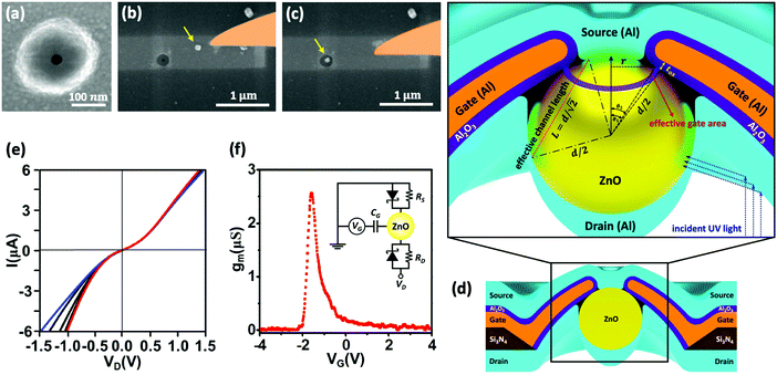 |
| | Fig. 2 (a) SEM image of a nanopore on a Si3N4 membrane. (b and c) SEM images of manipulating a single ZnO nanoparticle into the bottom side of the nanopore by using an optical fiber nanoprobe. (d) The cross-section schematic of the device containing a single ZnO nanoparticle surrounded by gate electrode and sandwiched between source and drain electrodes. Enlarged image shows the effective channel length between the source and drain, and the effective gate oxide area between the Al gate electrode and the ZnO nanoparticle. (e) I–VD characteristics at VG varying from −4 V (blue curve) to 4 V (red curve) with step 2 V at room temperature. (f) Transconductance as a function of VG at VD = −1 V. Inset is a schematic DC circuit model; RD and RS are shunt resistances at the drain and source electrodes, respectively. | |
Results and discussion
IV characteristics
Two devices, named as device A and B, were characterized and discussed here. The diameters of the embedded ZnO nanoparticles in these two devices are 70 nm and 80 nm, respectively. Due to the interface between the ZnO semiconductor and low electronegativity of Al, the contacts between them form Schottky barriers.18 Furthermore, owing to unavoidable leakage in the barriers, the Schottky diodes are shunted with leak resistors, denoted as RS and RD for top and bottom contacts, respectively. We thus modeled a DC circuit as shown in the inset of Fig. 2f. The RS and RD are highly temperature dependent, and the values increase at low temperatures. Because the contact area at the top (source) is much smaller than that at the bottom (drain), RD is much smaller than RS. Therefore, the drain contact behavior is more like an Ohmic contact but with a very small Schottky barrier whereas the source contact behavior is as a Schottky diode. Fig. 2e shows room-temperature I–VD curves measured at different gate voltages for device A. At positive bias (VD > 0), the source diode is reversely biased so that the current is mainly contributed by both shunt resistors RS and RD, and the device exhibits little gate voltage modulation. At negative bias (VD < 0), the source diode is put in forward bias and contributes to the current. The detailed current routes in two scenarios can be seen in Fig. S2 (ESI†). Since the Schottky barrier height can be tuned by gate voltage VG, the device shows obvious gate modulation. From that, we can judge that the ZnO nanoparticles are n-type behaviors. As illustrated in Fig. 2d, the ZnO nanoparticle is surrounded by the gate electrode, giving a strong capacitive coupling and a high transconductance (gm = dI/dVG).20–22Fig. 2f displays transconductance as a function of gate voltage and it reaches a maximum value of about 2.56 μS at VG = −1.6 V for device A, while 2.7 μS at VG = 0.8 V is obtained for device B shown in Fig. S3 (ESI†).
Mobility
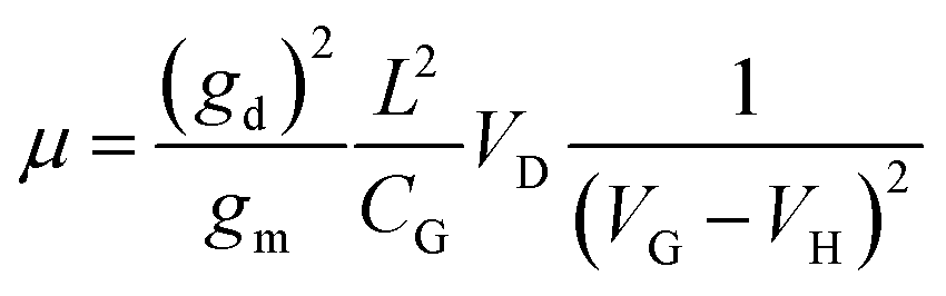
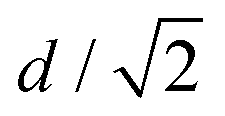
We further analyzed carrier mobility of ZnO nanoparticle devices. By considering the total contact resistance (RC = RS + RD) at the source and drain as shown in the inset of Fig. 2f, the current I at fixed bias voltage (VD) can be calculated using the following equation:| |  | (1) |
Here n = CG(VG − VTH)/eπr2L is the carrier concentration and μ, CG, L and VTH are carrier mobility, gate capacitance, channel length and threshold voltage, respectively. The carrier mobility can be evaluated as
| | 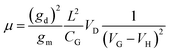 | (2) |
where
gd is differential conductance defined as
gd = d
I/d
VD and length
L is roughly

as illustrated in Fig. S4 (ESI
†), where
d is the particle diameter.
23–25 The gate capacitance
CG can be calculated using an effective gate area illustrated in the enlarged image of
Fig. 2d with an assumption that the contact angle is between 7–10 degrees and the oxide thickness is between 6–8 nm.
where
A and
tox are the effective gate oxide area and the insulating layer thickness, respectively.
The effective gate area can be determined as:
| |  | (4) |
where
d is the diameter of a ZnO nanoparticle. For device A,
θ1 = 25.4° (sin
θ1 = 2
r/
d,
r is nanopore radius) is a contact angle defined by the nanopore. If we assume that the contact angle between the gate oxide electrode and nanoparticle is between 7 and 10 degrees, corresponding to a tangent arc between 4 and 6 nm, then the effective gate area should be
A = 462–685 nm
2. With the Al
2O
3 layer thickness (
tox) of 6–8 nm and Al permittivity (
εrε0 = 8.27 × 10
−20 F nm
−1), the value of
CG = 5–9 aF can be obtained. Using the same approach, the gate capacitance for device B is determined to be 6–11 aF. Accordingly, the calculated mobility values for devices A and B are around 273–569 cm
2 V
−1 s
−1 which are one order higher than those of a synthesized ZnO single nanowire
26,27 and comparable to a nanosheet.
28 The high mobility values in our devices can be attributed to the elimination of grain boundary scattering as electrons transport through a single nanoparticle. Furthermore, the carrier concentrations are also calculated to be in the range of (4.4–8.0) × 10
17 cm
−3 and (3.7–6.8) × 10
17 cm
−3 for devices A and B, respectively. The estimated physical parameters of the two measured devices are listed in
Table 1.
Table 1 The estimated physical parameters of the two measured devices
| Device |
d/2 (nm) |
C
G (aF) |
g
m (μS) |
μ (cm2 V−1 s−1) |
n (cm−3) |
| A |
35 |
5–9 |
2.56 |
273–492 |
(4.4–8.0) × 1017 |
| B |
40 |
6–11 |
2.7 |
310–569 |
(3.7–6.8) × 1017 |
Temperature dependence
Fig. 3a and b display I–VD and I–VG characteristics at different temperatures for device A. It is found that the current decreases upon cooling due to decreased carrier concentration, giving rise to a threshold voltage shift in I–VG. Furthermore, decreased carrier concentration also causes both the Schottky barrier height and contact resistance to increase, resulting in prominent rectifying behavior. The calculated carrier concentration and electron mobility at different temperatures for both devices are plotted in Fig. 3c and d, respectively. It is noted that the carrier concentration decreases with decreasing temperature, as expected for semiconductor materials. Furthermore, the initial electron mobility increases and reaches a peak of 1070 cm2 V−1 s−1 (for device A) at around 180 K, referred to as Tcr, which is the crossover temperature that separates high-temperature electron–phonon scattering from low-temperature Coulomb scattering mechanisms. The initial increase at T > Tcr (from 300 K to Tcr) is originated from suppression of electron–phonon scattering.12,29,30 Below Tcr, the decrease in carrier concentration weakens the shielding effect and thereby promotes carrier–carrier and carrier–impurity Coulomb scatterings. Consequently, the carrier mobility decreases with decreasing temperature.12,29,31 Since Tcr is determined by the onset of the screening effect, it is carrier concentration-dependent, and the higher the carrier concentration the lower the crossover temperature. This can explain a lower Tcr observed for device A as compared to the behaviors from device B. Similar dependence of Tcr on carrier concentration was reported in ref. 32.
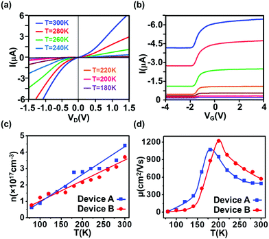 |
| | Fig. 3 (a) I–VD characteristic at VG = −1.6 V and (b) I–VG characteristic at VD = −1.0 V for device A at different temperatures. In both plots, the magnitude of the current decreases as the temperature is lowered from 300 K (blue curve) to 180 K (purple curve) in a step of 20 K. (c) Temperature dependence of carrier concentration and (d) electron mobility for both devices. The crossover temperature Tcr, at which the maximum mobility appears, is 180 K for device A and 200 K for device B, respectively. | |
Photoresponse
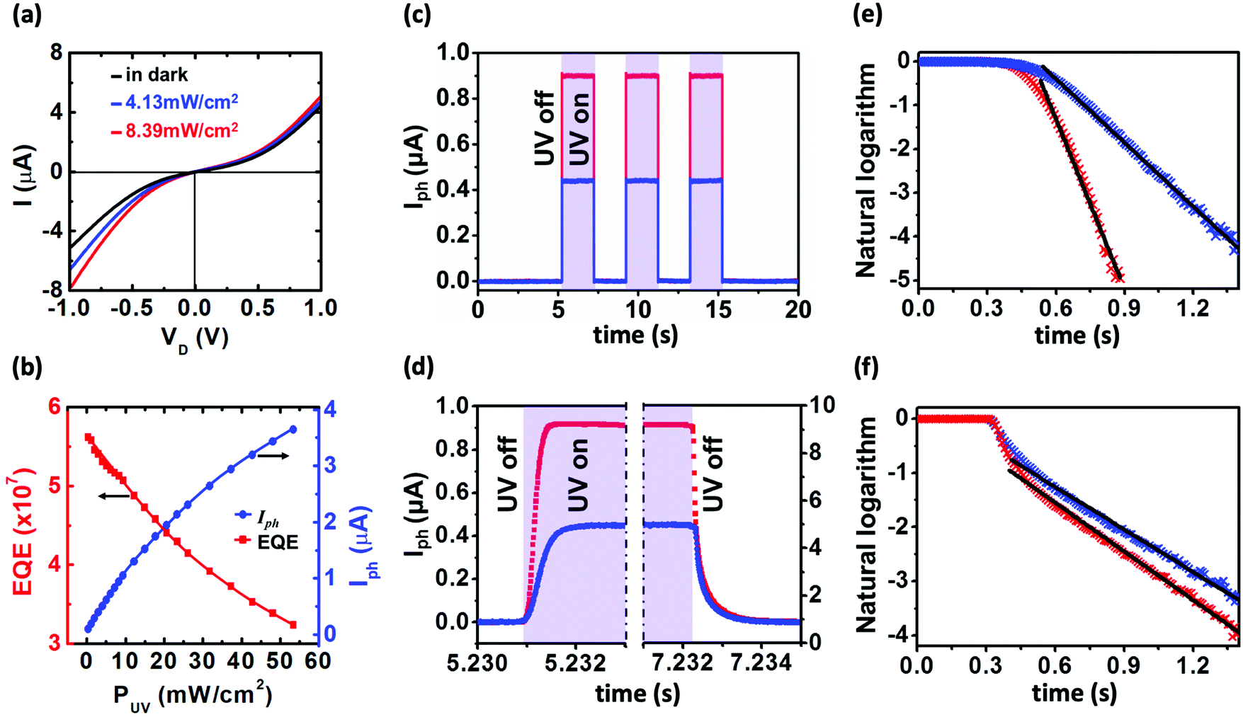
To explore the effects of high mobility on optoelectronic properties, the photoresponse of the devices is investigated. It is well known that because of the high surface-to-volume ratio, surface trap states drastically affect the transport and photoconduction properties of nanoparticles. Owing to the high electronegativity of ZnO, adsorbed oxygen molecules on the nanoparticle surface tend to attract electrons, forming disordered surface potential and suppressed electrical conductivity. Photo-excitation with energy above the energy gap of ZnO generates electron–hole pairs, and promotes electrical conduction in two ways: (1) the excited holes neutralize the negative oxygen ions and decrease surface charge scattering, and (2) the excited free carriers contribute to the conduction.26,33Fig. 4a displays the effect of photo-excitation on the I–VD characteristics by using UV-LED with a center wavelength of 365 nm (∼3.4 eV). It is noted that the higher the illumination intensities, the larger the generated photocurrents. Besides, owing to the asymmetric contact between ZnO and source/drain electrodes, the larger Schottky barrier at the source electrode can amplify the photodiode behavior. Therefore, an additional current will be generated at negative bias while the device is illuminated, resulting to a larger modulation in the negative direction compared to the positive direction.
 |
| | Fig. 4 (a) I–VD characteristics of device B under 365 nm UV-LED illumination with different intensities. The black curve is the I–VD in the dark whereas blue and red curves are for LED intensities of 4.13 mW cm−2 and 8.39 mW cm−2, respectively. (b) Illumination intensity dependence of external quantum efficiency (red squares) and photocurrent (blue dots). The measurements are performed at 300 K. (c–f) Photoresponse characteristics of device B under 365 nm UV-LED illumination at VD = −0.5 V at 300 K. Blue and red curves are for illumination intensity of 4.13 mW cm−2 and 8.39 mW cm−2, respectively. (c) On/off response of the photocurrent. The photocurrent is defined as Iph = Iill − Idark. (d) Magnified time scale showing rise and decay behaviors. Shaded area represents UV on. (e and f) Fittings to photocurrent rise and decay curves. | |
External quantum efficiency (EQE) or photo gain,26,28,34–36 defined as the ratio between the number of collected electrons induced by an incident photon per unit time, can be determined by using the following equation:
| |  | (5) |
where
Iph is photo-induced current and
Pill is incident illumination power on the particle;
h,
c, and
λ are Planck's constant, speed of light and incident light wavelength, respectively.
Iph =
Iill −
Idark, where
Iill and
Idark are illumination current and dark current, respectively. It is found that the obtained EQE is as high as 5.6 × 10
7 for a light intensity of 0.42 mW cm
−2, which is comparable to the reported values for other nano-structured inorganic semiconductors such as ZnO nanowires,
26,34 ZnO nanosheet,
28 In
2Ge
2O
7 nanobelts
35 and SnO
2 nanowires.
36 The high EQE can be attributed to the following origins: (1) large surface-to-volume ratio that enhances photo-excitation efficiency, and (2) the intrinsically defect-free nature of single crystalline and the short travelling distance that help to facilitate transport of carriers.
Fig. 4b shows light intensity dependence of
Iph and EQE values. It is noted that with increasing light intensity,
Iph increases while the EQE value decreases. Similar EQE behavior was reported and attributed to the increase in the recombination probability of excited-carriers, which shortens the carrier lifetime,
26,35,36 and a sufficient number of photogenerated holes being more than the number of trap sites, leading to lower trapping possibility.
37,38
The main figures of merit for photodetectors are responsivity (R) and specific detectivity (D*).39 The estimation shown below is for device B. For the responsivity, it can be determined as
| |  | (6) |
where
S is the effective illuminated area of the ZnO nanoparticle. To estimate the specific detectivity, we assume that the shot noise from the dark current is the main contribution to the noise,
40 the specific detectivity can be calculated by
| |  | (7) |
where
e is the elementary charge and
Idark is the dark current which is around 4 μA at
VD = 1 V. The effective illuminated area
S is assumed around a quarter the surface area of the nanoparticle by considering light only penetrating from the estimated penetration depth of aluminum around the side wall as shown in Fig. S5 (ESI
†). According to the above equations,
R and
D* are up to 1.39 × 10
6 AW
−1 and 8.69 × 10
12 Jones, respectively.
Photoresponse time of the device is also studied. Fig. 4c presents the time-resolved photocurrent under a fixed reversed bias voltage at different UV-LED intensities. The photo switching is stable and reproducible. The magnified time scale shown in Fig. 4d clearly indicates photocurrent transient characteristics. The rise and decay times can be obtained by fitting the photocurrent data (blue and red crosses) to exponential growth [I = Iph(1 − e−t/τ)] and decay [I = Iph(e−t/τ)] functions (black lines), where τ is a time constant, as shown in Fig. 4e and f, respectively. From these fittings, the rise times for low and high intensities are 0.21 ms and 0.09 ms, respectively. However, the decay time does not change much with the intensity. For low and high intensities, they are 0.37 ms and 0.35 ms, respectively. Both time scales (well below 1 ms) are much faster than those of other ZnO nano-structures such as nanowires,26,27,33,34,41 nanosheet,28 and thin films.42–46 This fast photoresponse behavior is similar to the previous reference and can be attributed to short traveling distance where the carrier scattering is relatively lower.46 It is also noted that the higher the UV-illumination intensities the faster the rise time. This originates from the higher energy to easily tunnel the barrier height leading to a reduction of contact resistance effectively at the metal–semiconductor interfaces. For comparison between our results and other works, the electrical and optical properties for different types of ZnO nano-structures are shown in Table 2 in which the most prominent is ultrafast response time in this work.
Table 2 Comparison of electrical and optical properties for different types of ZnO nano-structures
| Ref. |
Type |
μ (cm2 V−1 s−1) |
n (cm−3) |
g
m (μS) |
QE (photo gain) |
Responsivity (AW−1) |
Detectivity (Jones) |
Response time |
|
26
|
Nanowire |
270 |
∼1013 |
— |
IQE: 2 × 10⁸ |
— |
— |
Rise: 23 s, decay: 33 s |
|
27
|
Nanowire |
25–33 |
∼1016 |
— |
— |
1.6 × 10⁶ |
— |
— |
|
28
|
Nanosheet |
609 |
— |
— |
— |
6.83 × 10³ |
6.11 × 10¹⁴ @1 V bias |
Rise: 300 ms, decay: 310 ms |
|
34
|
5 Nanowires (in parallel) |
— |
1.6 × 10¹⁷ |
— |
IQE: 2.6 × 10⁷ |
7.5 × 10⁶ |
3.3 × 10¹⁷ @1 V bias |
Rise: 560 ms, decay: 320 ms |
|
44
|
Thin film |
— |
— |
— |
— |
∼0.11 |
2 @1 V bias |
5 ms |
|
46
|
Thin film |
— |
— |
— |
— |
1 × 10³ (VW−1) |
— |
Rise: 51 ms, decay: 69 ms |
| This work |
Nanoparticle |
∼600 @300K, ∼1100 @180K |
8 × 10¹⁷ |
∼2.6 |
EQE: 5.6 × 10⁷ |
1.39 × 10⁶ |
8.69 × 10¹² @1 V bias |
Rise: 0.09 ms, decay: 0.35 ms |
Conclusions
In summary, high mobility single ZnO nanoparticle transistors are fabricated. The devices exhibit high electron mobility due to elimination of scattering resulting from defects and grain-boundaries. Upon cooling from room temperature, the mobility first increases due to suppressed electron–phonon scattering and then decreases at low temperatures due to enhanced Coulomb scatterings. With such high mobility, the device not only shows high responsivity of 1.39 × 10⁶ and EQE values of 5.6 × 10⁷, but also exhibits an ultrafast photoresponse time of 0.09 ms for the rising time due to short traveling distance. These characteristics greatly increase the potential applications of single semiconductor nanoparticles in transistors and optoelectronics.
Conflicts of interest
There are no conflicts to declare.
Acknowledgements
We thank Tzu-Hui Hsu and Yu-Cheng Chang for their assistance during the course of this work. This research was funded by the National Science Council of Taiwan under contract No. NSC 98-2112-M-001-023-MY3, NSC 100-2120-M-002-002 and MOST 105-2112-M-003-016-MY3, and by Funds for Science and Technology Development of the University of Danang under project number B2018-DN06-11. Technical support from NanoCore, the Core Facilities for Nanoscience and Nanotechnology at Academia Sinica, is acknowledged.
References
- G. Zhu, R. Yang, S. Wang and Z. L. Wang, Nano Lett., 2010, 10, 3151–3155 CrossRef CAS PubMed.
- M. Law, L. E. Greene, J. C. Johnson, R. Saykally and P. D. Yang, Nat. Mater., 2005, 4, 455–459 CrossRef CAS PubMed.
- S. Chu, G. Wang, W. Zhou, Y. Lin, L. Chernyak, J. Zhao, J. Kong, L. Li, J. Ren and J. Liu, Nat. Nanotechnol., 2011, 6, 506–510 CrossRef CAS PubMed.
- H. Kind, H. Q. Yan, B. Messer, M. Law and P. D. Yang, Adv. Mater., 2002, 14, 158–160 CrossRef CAS.
- H. Frenzel, A. Lajn, H. von Wenckstern, M. Lorenz, F. Schein, Z. Zhang and M. Grundmann, Adv. Mater., 2010, 22, 5332–5349 CrossRef CAS.
- H. Bong, W. H. Lee, D. Y. Lee, B. J. Kim, J. H. Cho and K. Cho, Appl. Phys. Lett., 2010, 96, 192115 CrossRef.
- R. L. Hoffman, J. Appl. Phys., 2004, 95, 5813–5819 CrossRef CAS.
- E. M. C. Fortunato, P. M. C. Barquinha, A. Pimentel, A. M. F. Goncalves, A. J. S. Marques, R. F. P. Martins and L. M. N. Pereira, Appl. Phys. Lett., 2004, 85, 2541–2543 CrossRef CAS.
- W. I. Park, J. S. Kim, G. C. Yi, M. H. Bae and H. J. Lee, Appl. Phys. Lett., 2004, 85, 5052–5054 CrossRef CAS.
- P.-C. Chang, Z. Fan, C.-J. Chien, D. Stichtenoth, C. Ronning and J. G. Lu, Appl. Phys. Lett., 2006, 89, 133113 CrossRef.
- G. D. Yuan, W. J. Zhang, J. S. Jie, X. Fan, J. A. Zapien, Y. H. Leung, L. B. Luo, P. F. Wang, C. S. Lee and S. T. Lee, Nano Lett., 2008, 8, 2591–2597 CrossRef CAS.
- J. Goldberger, D. J. Sirbuly, M. Law and P. Yang, J. Phys. Chem. B, 2005, 109, 9–14 CrossRef CAS.
- H. Li, C. Liang, K. Zhong, M. Liu, G. A. Hope, Y. Tong and P. Liu, Nanoscale Res. Lett., 2009, 4, 1183–1190 CrossRef CAS.
- Z. L. Wang, J. Phys.: Condens. Matter, 2004, 16, R829–R858 CrossRef CAS.
- J. Liu, X. Huang, Y. Li, K. M. Sulieman, F. Sun and X. He, Scr. Mater., 2006, 55, 795–798 CrossRef CAS.
- D. Segets, J. Gradl, R. K. Taylor, V. Vassilev and W. Peukert, ACS Nano, 2009, 3, 1703–1710 CrossRef CAS.
- H. M. Yang, Biomed. Res., 2017, 28, 2262–2266 CAS.
- N. Linh-Nam, M.-C. Lin, H.-S. Chen, Y.-W. Lan, C.-S. Wu, K.-S. Chang-Liao and C.-D. Chen, Nanotechnology, 2012, 23, 165201 CrossRef.
- S. H. Brewer and S. Franzen, J. Alloys Compd., 2002, 338, 73–79 CrossRef CAS.
- S. N. Cha, J. E. Jang, Y. Choi, G. A. J. Amaratunga, G. W. Ho, M. E. Welland, D. G. Hasko, D. J. Kang and J. M. Kim, Appl. Phys. Lett., 2006, 89, 263102 CrossRef.
- J. Xiang, W. Lu, Y. Hu, Y. Wu, H. Yan and C. M. Lieber, Nature, 2006, 441, 489–493 CrossRef CAS.
- S. A. Dayeh, D. P. R. Aplin, X. Zhou, P. K. L. Yu, E. T. Yu and D. Wang, Small, 2007, 3, 326–332 CrossRef CAS.
- Q. Cao, S.-J. Han, G. S. Tulevski, A. D. Franklin and W. Haensch, ACS Nano, 2012, 6, 6471–6477 CrossRef CAS.
- Y. Xu, T. Minari, K. Tsukagoshi, J. A. Chroboczek and G. Ghibaudo, J. Appl. Phys., 2010, 107, 114507 CrossRef.
- G. Horowitz, R. Hajlaoui, D. Fichou and A. El Kassmi, J. Appl. Phys., 1999, 85, 3202–3206 CrossRef CAS.
- C. Soci, A. Zhang, B. Xiang, S. A. Dayeh, D. P. R. Aplin, J. Park, X. Y. Bao, Y. H. Lo and D. Wang, Nano Lett., 2007, 7, 1003–1009 CrossRef CAS.
- M. Y. Lu, M. P. Lu, S. J. You, C. W. Chen and Y. J. Wang, Sci. Rep., 2015, 5, 8 Search PubMed.
- Y. Wang, P. Wang, Y. K. Zhu, J. R. Gao, F. Gong, Q. Li, R. Z. Xie, F. Wu, D. Wang, J. H. Yang, Z. Y. Fan, X. Y. Wang and W. D. Hu, Appl. Phys. Lett., 2019, 114, 5 Search PubMed.
- T. Ando, A. B. Fowler and F. Stern, Rev. Mod. Phys., 1982, 54, 437–672 CrossRef CAS.
- R. Graham and D. Yu, Nano Lett., 2012, 12, 4360–4365 CrossRef CAS PubMed.
- M. H. Somerville, D. R. Greenberg and J. A. Delalamo, Appl. Phys. Lett., 1994, 64, 3276–3278 CrossRef CAS.
- I. G. Lezama, M. Nakano, N. A. Minder, Z. Chen, F. V. Di Girolamo, A. Facchetti and A. F. Morpurgo, Nat. Mater., 2012, 11, 788–794 CrossRef CAS PubMed.
- T. Zhai, X. Fang, M. Liao, X. Xu, H. Zeng, B. Yoshio and D. Golberg, Sensors, 2009, 9, 6504–6529 CrossRef CAS.
- X. Liu, L. L. Gu, Q. P. Zhang, J. Y. Wu, Y. Z. Long and Z. Y. Fan, Nat. Commun., 2014, 5, 9 Search PubMed.
- W. Tian, C. Zhi, T. Zhai, X. Wang, M. Liao, S. Li, S. Chen, D. Golberg and Y. Bando, Nanoscale, 2012, 4, 6318–6324 RSC.
- L. Hu, J. Yan, M. Liao, L. Wu and X. Fang, Small, 2011, 7, 1012–1017 CrossRef CAS.
- L. H. Zeng, L. L. Tao, C. Y. Tang, B. Zhou, H. Long, Y. Chai, S. P. Lau and Y. H. Tsang, Sci. Rep., 2016, 6, 20343 CrossRef CAS.
- O. Lopez-Sanchez, D. Lembke, M. Kayci, A. Radenovic and A. Kis, Nat. Nanotechnol., 2013, 8, 497–501 CrossRef CAS PubMed.
- Y. W. Lan, C. M. Torres, X. D. Zhu, C. L. Sun, S. L. Zhu, C. D. Chen and K. L. Wang, Nano Energy, 2016, 27, 114–120 CrossRef CAS.
- X. Gong, M. H. Tong, Y. J. Xia, W. Z. Cai, J. S. Moon, Y. Cao, G. Yu, C. L. Shieh, B. Nilsson and A. J. Heeger, Science, 2009, 325, 1665–1667 CrossRef CAS.
- J. B. K. Law and J. T. L. Thong, Appl. Phys. Lett., 2006, 88, 133114 CrossRef.
- L. J. Mandalapu, F. Xiu, Z. Yang and J. L. Liu, Solid·State Electron., 2007, 51, 1014–1017 CrossRef CAS.
- P. Sharma, K. Sreenivas and K. V. Rao, J. Appl. Phys., 2003, 93, 3963–3970 CrossRef CAS.
- E. Nurfani, M. A. K. Purbayanto, T. Aono, K. Takase and Y. Darma, Opt. Mater., 2018, 84, 453–458 CrossRef CAS.
- R. Khokhra, B. Bharti, H. N. Lee and R. Kumar, Sci. Rep., 2017, 7, 15032 CrossRef.
- H. K. Yadav, K. Sreenivas and V. Gupta, J. Appl. Phys., 2010, 107, 044507 CrossRef.
Footnote |
| † Electronic supplementary information (ESI) available. See DOI: 10.1039/c9nh00299e |
|
| This journal is © The Royal Society of Chemistry 2020 |
Click here to see how this site uses Cookies. View our privacy policy here. 
 *d
*d

 , where c is the speed of light and λ is the wavelength of the incident light; μAl and σAl are permeability and conductivity of aluminum, respectively.19 According to the schematic geometry in Fig. 2d, the drain electrode on the side wall of the nanoparticle could be below 2.86 nm while 30 nm thick metal was perpendicularly deposited on the top. Therefore, the UV light is able to penetrate through the metal and interact with the ZnO nanoparticle. All the electrical measurements were performed in a Physical Property Measurement System (PPMS from Quantum Design) with a homemade current–voltage amplifier.
 as illustrated in Fig. S4 (ESI†), where d is the particle diameter.23–25 The gate capacitance CG can be calculated using an effective gate area illustrated in the enlarged image of Fig. 2d with an assumption that the contact angle is between 7–10 degrees and the oxide thickness is between 6–8 nm.