
 Open Access Article
 This Open Access Article is licensed under a
 Creative Commons Attribution 3.0 Unported Licence
Thermal conductance between water and nm-thick WS2: extremely localized probing using nanosecond energy transport state-resolved Raman†
Hamidreza
Zobeiri‡
a,
Nicholas
Hunter‡
a,
Ridong
Wang‡
 b,
Xinman
Liu
c,
Hong
Tan
*d,
Shen
Xu
*ae and
Xinwei
Wang
*a
b,
Xinman
Liu
c,
Hong
Tan
*d,
Shen
Xu
*ae and
Xinwei
Wang
*a
aDepartment of Mechanical Engineering, Iowa State University, Ames, Iowa 50011, USA. E-mail: shxu16@sues.edu.cn; xwang3@iastate.edu; Tel: +1-515-294-8023
bState Key Laboratory of Precision Measuring Technology and Instruments, Tianjin University, Tianjin 300072, P. R. China
cDepartment of Landscape Architecture, University of Washington, Seattle, Washington 98105, USA
dSchool of Energy and Power Engineering, Nanjing University of Science and Technology, Nanjing 210094, P. R. China. E-mail: tanhongwh@njust.edu.cn
eAutomotive Engineering College, Shanghai University of Engineering Science, 333 Longteng Road, Shanghai 201620, People's Republic of China
First published on 2nd November 2020
Abstract
Liquid–solid interface energy transport has been a long-term research topic. Past research mostly focused on theoretical studies while there are only a handful of experimental reports because of the extreme challenges faced in measuring such interfaces. Here, by constructing nanosecond energy transport state-resolved Raman spectroscopy (nET-Raman), we characterize thermal conductance across a liquid–solid interface: water–WS2 nm film. In the studied system, one side of a nm-thick WS2 film is in contact with water and the other side is isolated. WS2 samples are irradiated with 532 nm wavelength lasers and their temperature evolution is monitored by tracking the Raman shift variation in the E2g mode at several laser powers. Steady and transient heating states are created using continuous wave and nanosecond pulsed lasers, respectively. We find that the thermal conductance between water and WS2 is in the range of 2.5–11.8 MW m−2 K−1 for three measured samples (22, 33, and 88 nm thick). This is in agreement with molecular dynamics simulation results and previous experimental work. The slight differences are attributed mostly to the solid–liquid interaction at the boundary and the surface energies of different solid materials. Our detailed analysis confirms that nET-Raman is very robust in characterizing such interface thermal conductance. It completely eliminates the need for laser power absorption and Raman temperature coefficients, and is insensitive to the large uncertainties in 2D material properties input.
1. Introduction
Thermal transport across a solid–liquid interface is a topic of ongoing research due to its various applications in micro/nanoscale thermal transport, such as evaporation cooling and energy conversion,1–5 thermal management,6–8 ultrafast flow delivery,9 cancer treatment,10 solar thermal heating,11 and nanofluids.12,13Continuum based interface thermal resistance (ITR) models describe this resistance as an irruption on phonon propagation in a crystalline lattice. This is due to the difference in the speed of sound between two materials which leads to a mismatch in acoustic impedance.14 The Acoustic Mismatch Model (AMM) and the Diffuse Mismatch Model (DMM) are the main models to explain this mismatch across a solid–liquid interface and have been used widely for the theoretical calculation of interface thermal transport.15 The AMM model neglects phonon scattering at the interface, while the DMM model considers their diffuse scattering across the interface.16,17 AMM and DMM predict high and low interface thermal resistance, respectively, which provide upper and lower limits for the interface thermal resistance. However, these two models do not consider surface complexities and solid–liquid interaction strength. Molecular dynamic (MD) simulation is an alternative method for studying ITR theoretically without considering continuum based governing equations, and it is capable of studying several factors that can affect the ITR, such as surface wettability. Note that in some calculations the term Kapitza length lK is used to represent the ITR quantitatively. lK is defined as: lK = RKk, where RK is ITR or Kapitza resistance and k is the thermal conductivity of one of the phases, usually the liquid. Barrat et al. studied the dependence of RK on wetting properties using non-equilibrium MD simulation as a function of the interaction coefficient (c12) of the Lennard-Jones equation and under normal pressures. Their results showed relatively large values of RK when the liquid is not wetting the solid (small c12 values).18 They reported that lK decreased from 50 nm to less than 10 nm, as the c12 coefficient increased from 0.5 to 1. Kim et al. investigated the interface thermal transport between parallel plates separated by a thin layer of liquid argon using a 3D MD simulation employing 6–12 Lennard-Jones potential interactions, and studied lK as a function of surface wettability, thermal oscillation frequency, wall temperature (from 80 to 160 K), and channel height. They assumed that the solid molecules had the same mass as the argon molecules. Their results indicated that lK varies from 1 to 10 nm under several scenarios.19 Similar results were reported by Giri et al. and Vo et al. regarding the effect of interaction strength and thermal boundary conductance.20,21 In another work, RK was reported in the range of 5 × 10⁻⁸ to 4 × 10⁻⁷ m2 K W−1 using non-equilibrium MD simulations at liquid–vapor Ar mixtures adjacent to warmer Fe walls.22 Murad et al. studied the ITR between Si and water using MD simulation, and they found that RK decreases with increasing temperature from 5 × 10⁻⁶ m2 K W−1 to 3 × 10⁻⁹ m2 K W−1 when temperature increases from ∼350 K to ∼550 K.23 In the work by Shenogina et al., it is reported that the Kapitza conductance is proportional to the work of adhesion, and for a highly hydrophilic surface it can be up to ∼160 MW m−2 K−1.24 Barisik et al. performed MD simulations of heat conduction in liquid Ar that is confined in Ag nano-channels and reported that RK can vary from 0.8 × 10⁻⁹ to 5 × 10⁻⁹ m2 K W−1 from cold to hot surface temperature, respectively.25 In another work they utilized MD simulations to study ITR at Ar–Ag and Ar–graphite interfaces, and concluded that lK increases with increased wall temperature, and is three times larger at an Ar–graphite interface than that at an Ar–Ag interface which is due to the difference between the interaction potentials of the molecular pairs in the two cases.16 While the last two works were conducted under generally low temperatures (∼130 K), Barisik et al. conducted other MD simulations and reported that lK at Si–water in a higher temperature range (more than RT) decreases slightly with increased wall temperature, and is on average around 9 nm.26 The pressure dependence of ITR at Au–water and Si–water interfaces was studied using MD simulations by Pham et al.27 Their results revealed that the pressure dependence of lK depends on surface wettability. The lK of the Au–water (hydrophobic) interface was stable despite increasing water pressure, while it changed significantly across an Si–water interface (hydrophilic). Han et al. drew the same conclusion that ITR increases with liquid pressure enhancement through an MD simulation of n-perfluorohexane in contact with gold.28 The ITRs of several linear alkane liquids in contact with gold were obtained using non-equilibrium MD by Bin Saleman et al. They found that ITR is directly proportional to the number of carbon atoms in an alkane molecule and on average is ∼1.5 × 10⁻⁷ m2 K W−1.29
Past discussion was mostly focused on theoretical works, especially MD simulations. Unfortunately, there are only a few experimental works in the field of solid–liquid ITR measurement to compare with those calculated values. In 2002, M. Wilson et al. investigated thermal interface conductance between Au, Pt, and AuPd nanoparticles suspended in water or toluene. They found a thermal conductance (G) of 130 MW m−2 K−1 for a citrate-stabilized Pt nanoparticles and water interface by heating particles with a 770 nm optical laser and interrogating the decay of their temperature through time-resolved changes in optical absorption.30 In their next work, the effect of the organic stabilizing group on the G of AuPd particle–water and AuPd particle–toluene interfaces was studied with a similar technique.31 Two conclusions were arrived at in their work: (1) the values of G of the particle–water interface under different stabilizing groups were in the order of 100–300 MW m−2 K−1, which means that G is large, regardless of the self-assembled stabilizing group, and (2) the G of an AuPd particle–water interface was larger than that of an AuPd particle–toluene interface, which indicates the effect of the liquid phase on ITR. In another work, Ge et al. performed a similar time-domain thermoreflectance technique and studied the effects of surface wettability on lK using Au and Al based surfaces. The results indicated that lK at hydrophobic (Al) interfaces (10–12 nm) is a factor of 2–3 larger than lK at hydrophilic (Au) interfaces (3–6 nm), which is in agreement with MD simulations.32 Park et al. reported ITR studies for a system of Au nanorods immobilized on a crystalline quartz support and immersed in various organic fluids by heating the nanorods with a subpicosecond optical pulse and monitoring their cooling process by transient absorption.33 They found the thermal conductances of the nanorod–fluid interface at 36 ± 4 MW m−2 K−1, 32 ± 6 MW m−2 K−1, 30 ± 5 MW m−2 K−1, and 35 ± 4 MW m−2 K−1, for methanol, ethanol, toluene, and hexane, respectively. This indicated that G drops significantly as water is replaced by an organic fluid. Using a similar technique, it was reported that the G of Au nanodisks coated with a hydrophilic self-assembled monolayer varies over 90–190 MW m−2 K−1, depending on the amount of water in the liquid mixture. For hydrophobic surfaces, G is in range of 70 ± 10 MW m−2 K−1. This was attributed to the effects of the work of adhesion on interface thermal conductance.34
Raman spectroscopy has proved to be a powerful tool for studying thermal transport at micro/nanoscales. Several works have been reported that show the potential of this tool to investigate the thermal conductivity and hot carrier diffusion coefficient of 2D materials, such as graphene35,36 and transition metal dichalcogenides (TMD).37–40 Raman spectroscopy is able to measure the ITR of solid–solid interfaces, as well as the aforementioned properties. Yuan et al. reported the interface thermal conductance between few-layered to multi-layered MoS2 films and Si, and showed that G increases with an increased number of layers of MoS2 thin film from 1 to 69 MW m−2 K−1.41 They reported other works that successfully measured the ITR between thin layers of TMD materials and a glass or Si substrate.42–44 Raman spectroscopy based techniques have the advantage of being non-contact, non-invasive, and material-specific leading to higher accuracy of measured parameters.
In this work, for the first time, the interfacial thermal conductance (Gint) between de-ionized (DI) water and WS2 nm-thick film is measured using a novel nanosecond energy transport resolved Raman (nET-Raman) technique. Each WS2 sample is suspended over a hole, and immersed in a water bath. Using this experimental structure, WS2 film is in contact with water from the top, while its other side is isolated thermally by air inside the hole. Interfacial thermal transport between solid and liquid is characterized here for three samples of different thicknesses. The measured Gint is compared and verified with other literature values based on both experimental and MD methods. It is shown in detail that the accuracy of the measurement can be improved by using shorter laser pulses as the transient part of the Raman thermometry. Also, it is proved that uncertainties in the laser absorption coefficient, Raman temperature coefficient, and values of thermal properties of WS2 film in theoretical calculations do not downgrade the precision of characterization. In the following, the feasibility and capability of this method are explored in detail.
2. Materials preparation and theoretical basis
2.1. Sample preparation
Two different sizes of holes are made on an Si substrate using FIB to prepare the suspended samples. One of the holes is circular with a diameter of 10 μm and the other one is square with 22 μm side length. Fig. 1 shows the cross-sectional view of the hole that is used to suspend the sample on top of it. Then, three nm-thick WS2 flakes are prepared using the mechanical exfoliation method from bulk WS2, which guarantees the quality and crystallinity of the layers. Mechanical exfoliation makes it possible to prepare several samples of different thicknesses depending on the force applied to the bulk sample. Finally, these samples are transferred to the holes by gel-films and a 3D micro-stage. More details of this process can be found in our previous work.45,46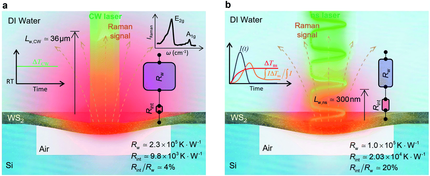 | ||
| Fig. 1 Cross-sectional view of the experimental sample design to measure the interfacial thermal conductance (Gint) at a water–WS2 nm-thick film interface. The nm-thick WS2 film is suspended over a hole in an Si layer. The hole depth is 3 μm. A graphical illustration of the effects of relative contribution of total interface resistance (Rint) and water thermal resistance (Rw) under (a) CW and (b) ns heating states. Under each state, the WS2 film is irradiated using a specific laser and the Raman signal is collected. A sample Raman spectrum of WS2 is shown in the inset of figure (a). Under CW laser heating, Rint is ∼4% of Rw, showing it has a weak effect on total thermal resistance between the WS2 sample and DI water, while under the ns laser this ratio is ∼20%. As a result, we expect to observe the effects of Rint on the temperature evolution of WS2 film under the ns heating state. Also, these two figures represent the thermal diffusion to the water and the fact that Lw,ns is much shorter than Lw,CW. The red thermal contour in each figure shows this effect. Also, the time-dependent temperature evolution under laser irradiation is represented schematically in the inset of each figure. For the CW case, the temperature rise (ΔTCW) is constant due to the steady-state heating of this laser. The transient temperature rise and Raman weighted average temperature rise of the ns case are shown using red and orange curves in the inset of part (b). Also, the blue curve indicates a single ns laser pulse. | ||
The Si substrate with the WS2 film on top of it is mounted on a stage inside a glass container. This container is filled with DI water. Using this setup, the WS2 film is in contact with air from the bottom, while touching the water on top (Fig. 1). Comparing the heat transfer on both sides of the WS2 layer, this design guarantees that heat transfers to water as much as possible and maximizes the effect of the water–WS2 interface on the temperature evolution of the film. A glass slide is placed on top of the container to prevent water evaporation and to stabilize water inside the container. It should be noted that water will not penetrate underneath the WS2 layer in the first few hours during which the Raman experiment is being performed. We observe that after 24 hours or more, a few micro-bubbles are formed beneath the WS2 layer, which shows water penetration. As will be mentioned in the next section, the nET-Raman technique is based on the ratio of the temperature rise of the sample under two different heating states; therefore, any constant parameter that contributes equally under both states will have a negligible effect on the measured interface thermal resistance. Placing the glass substrate on top of the container obviously affects the laser power irradiating the sample, but since the transmission of the glass slide under two heating states is the same, it will not affect our measurement and is not considered in the characterization process.
This method can also be applied to other materials, such as bulk ones, by constructing an appropriate geometry. For instance, for bulk silicon with a thickness in the order of 100 s of micrometers, it is possible to drill/cut a hole at a micrometer dimension from the bottom of the Si, in such a way that only a thin layer of Si remains on the top, and its bottom is totally in contact with air. Again, by putting this sample inside a DI water chamber, its top surface will touch the water, and the interfacial thermal conductance between the Si layer and water could be measured.
2.2. Physical principles of nET-Raman
The temperature rise of the suspended sample under laser irradiation is directly related to the thermal conductivity of the WS2 film (k), the thermal conductivity of water, and the interfacial thermal resistance at the water–WS2 interface Temperature changes of the sample could be investigated by studying the frequency variation of Raman-active optical phonons under laser heating. In the nET-Raman technique, two different energy transport states are constructed to analyze the thermal response of the material. Under the first state, the thin sample is irradiated using a continuous-wave (CW) laser to construct steady-state heating. Under this state, the temperature rise of the sample is mainly controlled by the in-plane thermal conductivity of the sample (k) and the thermal conductivity of water. The second state, which is a transient state, is a nanosecond (ns) state. This state is constructed using a 300 kHz ns pulsed laser. Under this state, the temperature rise of the film receives more effects from
The contribution of  to the total thermal resistance between WS2 and water is more significant in the ns case than in CW. For the CW heating state and under the area of laser heating, the thermal resistance of water Rw could be estimated as: Rw = 1/(2DCWkw), where DCW and kw are the laser spot diameter of the CW laser under a 20× objective lens and thermal conductivity of water, respectively. Taking kw ≃ 0.6
![[thin space (1/6-em)]](https://www.rsc.org/images/entities/char_2009.gif) W m−1 K−1 for water, and DCW = 3.6 μm (Table 2, see below), Rw will be around 2.3 × 10⁵ K W−1. The total interface resistance (Rint) can be estimated as:
W m−1 K−1 for water, and DCW = 3.6 μm (Table 2, see below), Rw will be around 2.3 × 10⁵ K W−1. The total interface resistance (Rint) can be estimated as: 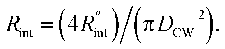 Take
Take  the total interface resistance will be around 9.8 × 10³ K W−1, which is 4% of the total water resistance covering the WS2 film. Therefore, the interfacial thermal resistance plays a negligible role compared with Rw in controlling the temperature of the WS2 film under the CW state and it is hard to detect its effects under this heating state [Fig. 1(a)]. It should be noted that performing the Raman experiment using a CW laser is necessary in this method, since it leads to the cancelling of the effects of several known and unknown parameters, such as laser absorption and temperature-dependent Raman coefficients, on the final results. This idea is represented in detail in the following paragraphs.
The laser pulse width (t0) of the ns laser used in this work is 212 ns. During ns laser pulse heating, the thermal diffusion length to the water layer can be estimated as: 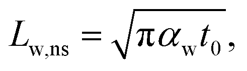 where αw is the thermal diffusivity of water. Lw,ns is around 300 nm. The total thermal resistance caused by water under the ns state is estimated as: Rw = 4Lw/(πDns2kw), where Dns is the laser spot diameter of the ns laser under a 20× objective lens, which is around 2.5 μm. Rw under this state is ∼100 × 103 K W−1. While this time Rint, using the same estimation as in the CW case and taking Dns as 2.5 μm (Table 2), is ∼20.3 × 10³ K W−1, which is ∼20% of Rw [Fig. 1(b)]. Hence, we expect that
  will play an important role under transient heating in the thermal response of the sample. Fig. 1(a) and (b) show a graphical representation of the relative effects of Rw and Rint under both states on total thermal resistance. Also, note that the thermal diffusion length to water under the CW state can be estimated as: Lw,CW ≃ 10DCW, which is ∼36 μm. This significant difference between Lw,CW and Lw,ns is also schematically shown in these two figures by red thermal contours.
In both states, laser heating and Raman signal excitation take place simultaneously. Collecting this Raman signal under various laser powers could be used to track the temperature evolution of the sample. In fact, we can obtain the Raman shift power coefficient (RSC) under each state by irradiating the sample using several laser powers (P). RSC is defined as: ψCW = ∂w/∂P = α(∂w/∂T)f(k), where α and ∂w/∂T are the laser absorption coefficient and Raman shift temperature coefficient, respectively. Under an ns energy transport state, which is designed to probe localized heating, RSC can be obtained as:  where ρcp is the volumetric heat capacity of each WS2 thin film. The thermal conductance at the water–WS2 interface is defined as:
 These definitions of
  and Gint are consistent in the rest of this article. As mentioned earlier, due to the localized heating of the ns state, the contribution of
  to ψCW is almost negligible in comparison to ψns; therefore the Raman shift power coefficients are different under these two states. Note that the f and g functions depend on the thermal properties of the materials under each heating state, and are more complicated to solve analytically. Therefore, it is too complicated to show their analytical forms, and they have to be solved numerically.
Using the last two Raman shift power coefficients ψCW and ψns, a new experimental parameter is defined as: Θexp = ψns/ψCW, which is called the normalized Raman shift power coefficient. It can easily be shown that Θexp is only a function of k,  and ρcp. And it is no longer a function of the temperature dependent Raman shift coefficient or laser absorption coefficient. This is the beauty of the nET-Raman technique which makes it independent of the last two coefficients. α and ∂w/∂T are generally the main sources of error in steady-state Raman thermometry. Using a 3D numerical model that calculates the temperature rise of the sample under CW (ΔTCW) and ns (ΔTns) heating states, we can find the theoretical value of the temperature rise ratio (Θth) as: Θth = ΔTns/ΔTCW. Using known values for k and ρcp for water and WS2, a relationship between Θth and
  is found. Finally, this relationship is used to find the
  value that meets the condition: Θexp = Θth. As mentioned earlier, known values of k and ρcp are used here from the literature.39,47,48 In the discussion part, it will be shown that both of these values have a negligible effect on the uncertainty and value of measured
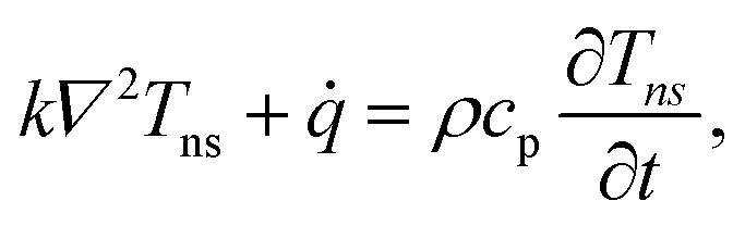
The first part of the 3D heat conduction model deals with steady-state heating under a CW laser, which is governed by the following differential equation:
k∇2TCW + ![[q with combining dot above]](https://www.rsc.org/images/entities/i_char_0071_0307.gif) = 0, = 0, | (1) |
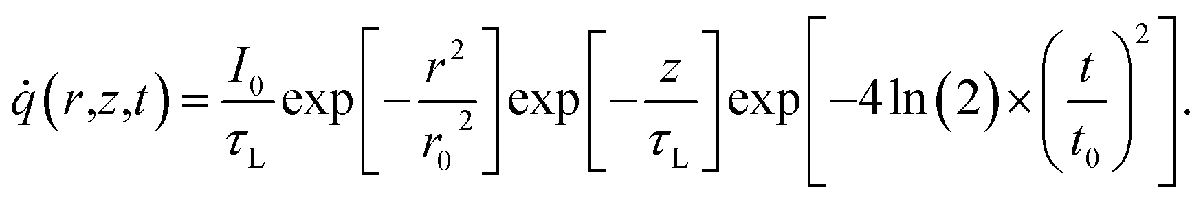
is the volumetric Gaussian beam heating, which is shown as: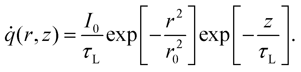 | (2) |
 value using the nET-Raman technique, since it will be canceled out by dividing the temperature rise under two heating states.48
Transient-state heating is generated using a 532 nm nanosecond laser with a 212 ns pulse width (t0). It should be noted that t0 should be smaller than the time needed for the sample to reach thermal equilibrium (teq). This time can be estimated as: teq ∼ (10r0,ns)2/αwater, where αwater is the thermal diffusivity of water. In this work, teq is around 25 ms, which is much larger than t0. Another point that is worth mentioning is the effect of hot carrier diffusion on thermal transport in this ns state. In short, as soon as the laser irradiates the WS2 sample, electrons in the valence band gain enough energy (more than the Fermi energy) to leave this band, leaving holes behind. These hot carriers recombine within a very short period of time (tl) which is in the order of 1 ns for WS2.51 Since tl is very much shorter than t0, we can ignore the effects of hot carrier diffusion on thermal transport. Hot carrier transfer inside TMD materials, such as WS2, was well-studied in our previous work.42,48,52 Regarding the thermal transport in the cross-plane direction of the WS2 sample, it is assumed that the temperature distribution in this direction is uniform. In the thickness direction, heat diffusion length (L⊥) under ns pulsed laser heating can be estimated as: 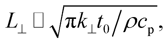 which is around 1 μm. Here, k⊥ is the thermal conductivity of WS2 in the cross-plane direction and is about 2 W m−1 K−1.53 This value is much larger than the thickness of all samples (Table 1, see below), which confirms the validity of this assumption. The governing equation of the ns laser heating state is:54
 | (3) |
 | (4) |
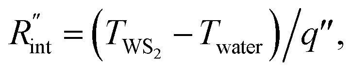 where q′′ is the interface heat flux. Note that Twater and TWS2 are the temperature of the water and WS2 film just close to the interface. Using the abovementioned equations, the temperature rise of the sample under two heating states could be calculated for different
  values. As mentioned earlier, the ratio of these calculated temperature rises of the two states is equal to the experimental normalized RSC for the objective
  It worth noting that the experimental RSC is based on Raman intensity-weighted temperature rises in both space and time domains and this point is considered in the theoretical calculation of the temperature rise under each state. Note that the temperature at the edge of the suspended area could be considered to be room temperature under both CW and ns cases for two main reasons. First, the interfacial thermal resistance at the WS2–Si interface at the edge is much smaller than the in-plane thermal resistance of the WS2 film. Second, the thermal resistance of Si is very low due to its high thermal conductivity. Therefore, it is reasonable to consider the room temperature boundary condition at the WS2–Si interface.
| Sample | Hole structure | Thickness (t) [nm] | Roughness (Rq) [nm] | (Rq/t) × 100 |
|---|---|---|---|---|
| 1 | Square | 88 | 6.20 | 7.04 |
| 2 | Circle | 33 | 4.54 | 13.7 |
| 3 | Circle | 22 | 2.44 | 11.1 |
3. Result and discussion
3.1. Sample characterization
Three suspended samples are prepared using the mechanical exfoliation method. Both AFM and SEM characterizations are performed to study the thickness and roughness profiles, and structure of these films. Fig. 2(a) shows the 2D AFM image of Sample 3 at the boundary of WS2 and the Si substrate. AFM measurements are conducted over the supported area to prevent sample damage. The thickness profile of this sample is shown in the figure using a gray 3D thickness profile and corresponds to the average thickness over the dotted rectangle in the direction of the arrow. The thickness of this sample is 22 nm. Fig. 2(b) indicates the 3D AFM image of this sample over a 10 μm × 10 μm area close to the suspended area. The root mean square (RMS) roughness of this sample is measured using this image and is 2.44 nm. Table 1 includes the thickness and roughness values of all samples, as well as the ratio of roughness over thickness. This ratio for all samples is less than 15%, which indicates good contact between the WS2 film and the Si substrate. | ||
| Fig. 2 (a) 2D AFM image of Sample 3 at the Si–WS2 boundary. The 3D thickness profile represents the average thickness of the sample over the dotted rectangular area. (b) AFM image of a supported area of this sample in the suspended area's neighborhood. The root mean square roughness (Rq) over this area is 2.44 nm. (c) The SEM image of the suspended area shows that this area is smoother and more uniform than the supported area. Also, it shows that the WS2 film is not totally flat and is a little bit concave toward the bottom of the trench. | ||
As will be discussed in the next section, sample roughness is one of the main parameters that can affect  In order to further study the sample's structure, we performed SEM measurement over the suspended area. Fig. 2(c) shows the SEM image of Sample 3. It shows that the suspended area is almost uniform in all directions. Also, it indicates that the sample is not totally flat over the hole, and is concave toward the bottom of the hole. This will affect the laser spot radius measurement and alter the actual size of the suspended area, and therefore the theoretical temperature rise calculation under both states will vary to some degree. This effect is discussed in detail in the next section.
3.2. Water–WS2 interface thermal conductance
A room temperature (RT) Raman experiment is conducted using both CW and ns lasers for all three samples to obtain the Raman shift power coefficient. For each sample, based on the WS2 film's structure and thickness, optimum laser power is used to find the Raman shift power coefficient with the highest accuracy. For both lasers, a 20× objective lens is used to focus the laser spot onto the surface of the WS2 film. This objective is chosen to minimize the effects of hot carrier diffusion on thermal transport. The hot carrier diffusion length (ΔrHC) is estimated as: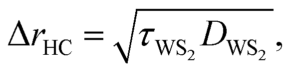 where DWS2 and τWS2 are the hot carrier diffusion coefficient and electron–hole recombination time, respectively. Using τWS2 and DWS2 from reference values, ΔrHC is ∼0.1 μm, which is much smaller than the laser spot radius under a 20× objective lens.48 Therefore, the hot carriers' effects on thermal transport are negligible in our experiment. The radius of the laser spot (r0) for each Raman experiment is measured by analyzing the optical images of the laser spots based on a Gaussian fitting method. Insets to Fig. 3(c) and (d) show the laser spots of both states for the third sample captured by a CCD camera. As mentioned in the previous section, knowing r0 for each heating state is necessary to simulate the heating process since it determines the in eqn (1) and (3). The laser spot size determines the laser intensity distribution while heating the sample, and, subsequently, the temperature rise and Raman shift. In this work, laser irradiation and laser spot measurement are conducted simultaneously, and the measured r0 is used directly in our numerical method. Therefore, any effects of laser spot size on our final result are considered precisely. The measured values of r0 at e−1 of the center intensity for all samples are shown in Table 2. Both lasers are operating at 532 nm wavelength. The ns pulsed laser's repetition rate is 300 kHz. For the ns laser, this repetition rate yields ∼4.7 W power at the peak of the laser pulse, and decreasing the repetition rate will increase this peak power and can cause sample damage. As will be shown in the next section, decreasing t0 without burning the film can reduce the uncertainty level of this technique. More information about the lasers and Raman system can be found in our previous work.46,55,56 Also, similar consideration should be involved in choosing the optimum CW laser power to prevent sample damage. Table 2 includes the laser power range for each sample under both heating states.
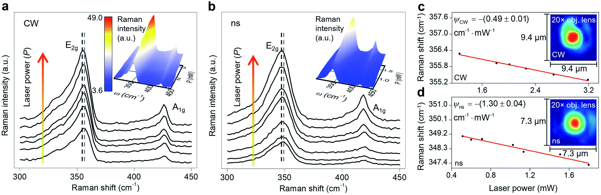 | ||
Fig. 3 Raman spectra of WS2 nm-film (Sample 3) under (a) CW, and (b) ns heating states. Both plots show that the Raman intensity of the E2g and A1g modes increases with increased laser power, and the peak position redshifts with the increased laser power. Here the E2g peak is used to perform the analysis and measure the interfacial thermal resistance  Two dashed lines in both figures indicate the redshift of the E2g peak. The insets of these two figures represent the 3D contour of Raman intensity as a function of peak position (ω) and laser power (P). These two contours confirm the aforementioned trends, as well as the linear increase in Raman intensity (I) with increased P. Note that the I value of the 3D contour of the ns state corresponds to the contour bar that is shown in the inset of part (a). The Raman shift power coefficient (ψ) corresponding to the E2g peak of WS2 under (c) CW and (d) ns laser of Sample 3. Black dots indicate the experimental position of the E2g peak at different laser powers, and the red line on each plot shows the fitted line to find the ψ value under each state. Note that the x-axis of both plots is the laser power just after the objective lens and before the laser beam enters the container. Hence, the absorbed laser power under each case is even lower. Since in the nET-Raman technique the ratio of these two RSCs is used to measure Two dashed lines in both figures indicate the redshift of the E2g peak. The insets of these two figures represent the 3D contour of Raman intensity as a function of peak position (ω) and laser power (P). These two contours confirm the aforementioned trends, as well as the linear increase in Raman intensity (I) with increased P. Note that the I value of the 3D contour of the ns state corresponds to the contour bar that is shown in the inset of part (a). The Raman shift power coefficient (ψ) corresponding to the E2g peak of WS2 under (c) CW and (d) ns laser of Sample 3. Black dots indicate the experimental position of the E2g peak at different laser powers, and the red line on each plot shows the fitted line to find the ψ value under each state. Note that the x-axis of both plots is the laser power just after the objective lens and before the laser beam enters the container. Hence, the absorbed laser power under each case is even lower. Since in the nET-Raman technique the ratio of these two RSCs is used to measure  the laser absorptions of the glass layer, DI water, and WS2 sample for each sample are identical for both heating states. This will not affect the determined the laser absorptions of the glass layer, DI water, and WS2 sample for each sample are identical for both heating states. This will not affect the determined  Ihe inset of each plot shows the laser spots that irradiate Sample 3 under a 20× objective lens for both CW and ns cases. Ihe inset of each plot shows the laser spots that irradiate Sample 3 under a 20× objective lens for both CW and ns cases. | ||
| Sample | CW laser spot radius [μm] | ns laser spot radius [μm] | CW laser power range [mW] | ns laser power range [mW] |
|---|---|---|---|---|
| 1 | 1.91 | 1.55 | 2.21–5.59 | 0.89–2.27 |
| 2 | 2.17 | 1.48 | 1.41–3.55 | 0.65–1.90 |
| 3 | 1.81 | 1.32 | 0.91–3.19 | 0.51–1.80 |
As shown in Table 2, the laser spot under the ns laser is smaller than that under the CW laser. This is caused by the collimation difference between the two laser beams. Also, the slight difference between r0 under each heating state is induced by a variation in focusing level. Note that all of these r0 values are more than the phonon mean free path (MFP) of the WS2 samples (∼15 nm);51,57,58 therefore, it is reasonable to assume that thermal transport is diffusive and under local-equilibrium. Additionally, these laser power ranges ensure the linear decrement of Raman shift against increased laser power with minimal local heating effects. Local heating effects induced at higher laser powers can alter the thermal properties of the WS2 film and reduce the quality of the experimental data. Note that these laser power ranges are for the laser beam before it reaches the glass cap on top of the substrate. The amount of laser power absorbed by each sample is even less than this and is ∼60%. All of these details are considered in the numerical calculation.
Sample 3 is used here to detail the data processing and the results. Fig. 3(a) and (b) show the Raman spectra of this sample under both heating states by varying the laser power. During the Raman experiment, we did not observe any significant auto-fluorescence in the background while collecting the Raman signal under both lasers. Each spectrum has two main Raman modes: E2g and A1g. E2g relates to in-plane vibrations and A1g represents the out-of-plane vibrations. Two dashed lines in this figure indicate the decrease in Raman shift of the E2g mode with increased laser power. The E2g mode is used in this work to find the Raman shift power coefficient, because it is stronger and more suitable for Raman peak fitting. Note that considering the A1g peak and performing the Raman experiment to find the RSC values will not affect the final results. This is shown by conducting nET-Raman using another sample (Sample 4), and the results are reported in ESI.† Ihe insets of these two plots show the 3D Raman intensity contour of this sample under CW and ns states. Also, they indicate that the Raman intensity of both E2g and A1g peaks increases linearly with increased laser power. It can be seen from both contours that both Raman peaks are red-shifted with increased laser power. 2D representations of these two contours are shown in Fig. S2 of ESI.† Note that each point's value in the 3D contour of the ns state follows the contour bar of the inset of Fig. 3(a). All representative Raman spectra of WS2, as shown in Fig. 3, are fitted using the Lorentzian function to find the exact Raman shift of the E2g peak at each laser power. The results of this peak fitting are shown in Fig. 3(c) and (d) for CW and ns heating states, respectively. The fitting quality depends on the quality of the experimental data and the Raman peak intensity. Generally, for intensities larger than a certain amount, the fitting quality will be almost intact. In this work, the integration time and laser power are chosen in such a way as to guarantee that the peak fitting uncertainty for low and high power cases are similar and less than 0.02 cm−1. Since this value is negligible, it is not included as the uncertainty of measured interface thermal conductance. As mentioned in the previous section, the slope of this line in the low power range indicates the RSC (ψ) value as: Δω = ψΔP, where ω is the Raman shift and P is the laser power. The ψ of the E2g mode under a CW laser is −(0.49 ± 0.01) cm−1 mW−1, and under the ns laser is −(1.30 ± 0.04) cm−1 mW−1. Similar results for all samples are included in Table 3. Note that ψ under the ns state is generally higher than the steady-state value. This is because for the same average power, the laser peak power of the ns laser is very high and induces a greater temperature rise. Also, the thermal diffusion length under this state is much smaller than the CW value. These two phenomena lead to the higher temperature rise under pulsed laser heating.
| Sample | Thickness [nm] | ψ CW [cm−1 mW−1] | ψ ns [cm−1 mW−1] | Θ exp |
|---|---|---|---|---|
| 1 | 88 | −(0.36 ± 0.01) | −(0.80 ± 0.02) | −(2.23 ± 0.09) |
| 2 | 33 | −(0.33 ± 0.01) | −(0.86 ± 0.03) | −(2.63 ± 0.14) |
| 3 | 22 | −(0.49 ± 0.01) | −(1.30 ± 0.04) | −(2.65 ± 0.11) |
It can be seen from this table that ψ generally increases with decreasing film thickness under each heating state. This is due to the fact that the temperature rise of each sample depends on the amount of absorbed laser energy, k, and thickness. The thickness affects the heat conduction in the sample and the laser absorption (multiple reflections in 2D samples and the optical interference effect). Note that for TMD materials, k increases gradually with increased thickness for samples of more than ∼5 nm and it reaches the bulk k value at larger thicknesses.45,59,60
A 3D numerical calculation based on the finite volume method is conducted to find  and consequently interfacial thermal conductance (Gint). The thermal properties of WS2 are held constant at: k = 32 W m−1 K−1, and ρcp = 1.92 × 10⁶ J m−3 K−1.47,48 Also, the thermal properties of DI water and air are taken from reference values. It will be shown in the following part of this work that uncertainties in these parameters have negligible effects on the determined
  or Gint and their uncertainties. Using this simulation, the Raman intensity weighted average temperature rise over both space and time domains for the ns state (Δ
![[T with combining macron]](https://www.rsc.org/images/entities/i_char_0054_0304.gif) ns), and only over space for the CW state (ΔCW), are calculated as:
ns), and only over space for the CW state (ΔCW), are calculated as:  respectively. These two temperature rises are shown schematically in the insets of Fig. 1. The exponential terms (e−z/τL) in these equations are related to the attenuation of the Raman signal as it leaves each scattering location. In these equations, I, V and ΔT represent the laser intensity under each state, sample volume, and temperature rise of each point, respectively. To match the laser intensity with experimental laser heating, the real laser spot radius, as shown in Table 2, is used to perform the simulation. This calculation is conducted for a range of
  values and Θth is calculated for each
  Finally, the resultant
  is deduced by equating Θth to Θexp. This process in shown in Fig. 4(a) for Sample 3. Also, the green area represents the uncertainty of the measured
  based on the uncertainty of Θexp, as indicated in Table 3. Measured
  values, as well as Gint, for all samples are summarized in Table 4.
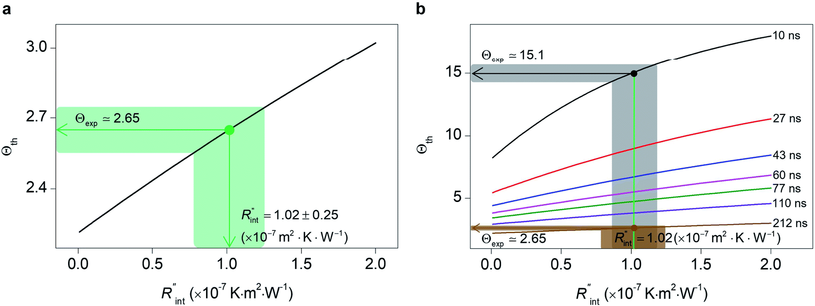 | ||
Fig. 4 (a) Measured  of Sample 3. The black line represents the theoretical Θ for several of Sample 3. The black line represents the theoretical Θ for several  values, and the green shaded area shows the uncertainty caused by the uncertainty in Θexp on values, and the green shaded area shows the uncertainty caused by the uncertainty in Θexp on  (b) Investigation of the effects of t0 on the uncertainty of (b) Investigation of the effects of t0 on the uncertainty of  determined using the nET-Raman technique. This plot shows that determined using the nET-Raman technique. This plot shows that  could be improved by ∼30% when t0 takes 10 ns compared with the could be improved by ∼30% when t0 takes 10 ns compared with the  of the default case where t0 is 212 ns. This is due to the higher contribution of of the default case where t0 is 212 ns. This is due to the higher contribution of  to the total thermal resistance between WS2 and DI water during shorter laser pulse heating. to the total thermal resistance between WS2 and DI water during shorter laser pulse heating. | ||
 and Gint for three suspended samples
| Sample | Thickness [nm] | Roughness (Rq) [nm] |
|
G int [MW m−2 K−1] |
|---|---|---|---|---|
| 1 | 88 | 6.20 | 0.85 ± 0.26 | 11.8 ± 3.60 |
| 2 | 33 | 4.54 | 4.00 ± 0.40 | 2.50 ± 0.25 |
| 3 | 22 | 2.44 | 1.02 ± 0.25 | 9.80 ± 2.40 |

It can be seen from this table that the Gint values of the three samples are almost in the same order, especially for samples 1 and 3. The larger resistance at the WS2–water interface of the second sample compared with the other samples could be caused by several factors. First, although the roughness of this sample is in the same order as that of the other two (Table 1), Rq is over the supported region close to the suspended area and the surface roughness of samples over the suspended region could be different than Rq, especially for the second sample.
3.3. Discussion
The measured Gint values in this work are in good agreement with the reference values of solid–water interface thermal transport measurements. Results from other work as well as the current work are summarized in Table 5.Comparing our result with other experimental work, it is obvious that the Gint of the WS2–water interface is an order of magnitude smaller than the Gint at AuPd–water or Pt–water interfaces, as shown in Table 5. The main factor that could contribute to this is the difference between the surface wettability of these three solids. Generally, Au and Pt possess smaller water contact angles than WS2, which means that these surfaces are more hydrophilic than a WS2 surface. For clean Au and Pt surfaces, the room temperature contact angle (θCA) at atmospheric pressure is in the range of 5–40°.61–65 While the θCA of multilayer WS2 at RT is around 50–80°.66,67 Also, in these works, the solid surfaces are more uniform and are in form of nanoparticles, and are smoother compared with the WS2 samples used in our experiment. θCA depends significantly on surface microscale roughness. As discussed in the introduction, hydrophobicity is one of the main parameters that affects the thermal transport at a solid–water interface and a lower θCA leads to stronger solid–water contact. A similar argument is valid regarding the Gint of ref. 27. Regarding the MD simulation results, it should be noted that ref. 26 reports Gint at several temperatures from 350 to 550 K, and at temperatures closer to RT, Gint is of the same order as our results.
As mentioned earlier, one parameter that affects the accuracy of our measurement is ns laser pulse width t0. As t0 takes smaller values, the thermal diffusion length in water will be shorter, and  contributes more to the thermal transport under the ns state compared with longer t0 cases. To show this fact, the temperature rise of the 22 nm sample under ns is calculated versus
 for several t0 cases ranging from 10 to 212 ns, and subsequently, Θth is calculated for each t0 case. Fig. 4(b) shows the result of this calculation. It is reasonable to see that Θth increases with decreased laser pulse width, since shorter pulses means higher pulse peak power that leads to a higher temperature rise. Also, as shown in Fig. 4(b), Θth is plotted for each case. This figure shows that the slope of each
  curve increases with decreased t0. Now, considering
  as indicated in Table 4, and assuming constant 5% uncertainty for each hypothetical Θexp value, we can find the uncertainty in
  for each t0 case. This is shown by the shaded areas in Fig. 4(b) for two extreme cases when t0 takes 212 ns and 10 ns. It is obvious that this area for smaller t0 values is narrower that for larger t0 values, which means higher accuracy in the measurement of
  As mentioned earlier, the
  ratio is ∼20% when t0 = 212 ns. Similar calculation shows that when t0 is 10 ns, this ratio is ∼60%, which indicates a higher contribution of interfacial thermal resistance to total thermal resistance between the WS2 film and water under ns laser heating. Note that under the ns pulsed laser that is used in this work, when t0 is 10 ns, the peak power of each laser pulse is ∼12 kW, and could damage the suspended film. Another note worth mentioning is that depending on the increment in laser intensity, the light absorption could be linear or non-linear. As long as the laser intensity is not so high as to make the light absorption non-linear, the laser pulse width could be decreased to increase the sensitivity of Gint measurement. An alternative way to implement this experiment with smaller pulse widths is using an amplitude modulated frequency laser, with appropriate frequency and narrow pulse. Under such conditions, the pulse width can be short enough to measure
  more accurately, while the laser power is kept below the damage threshold.
Another study is conducted to show that the nET-Raman technique does not depend on the known values of k and ρcp of the WS2 film. To do so, the temperature rise of Sample 3 under both heating states, and consequently Θth, are calculated for a range of k and ρcp. The results of this calculation are shown in Fig. 5. Using the Θexp of this sample (Table 3),  and its uncertainty are found for each case and represented by black solid line in each plot of Fig. 5. Two dashed lines show the uncertainty of measured
  corresponding to the uncertainty of Θexp. These two contours indicate that if k and ρcp of WS2 change by 10% independently, the resulting values of
  change by less than 2% and 4%, respectively. Also, the uncertainty of the measured
  will be almost intact, since the dashed lines and black solid line in each contour are almost parallel regardless of k and ρcp values. This figure indicates a critical fact that the effects of k and ρcp are almost canceled out by introducing Θ in this technique, and the three lines in each contour stay almost horizontal while k or ρcp is varied.
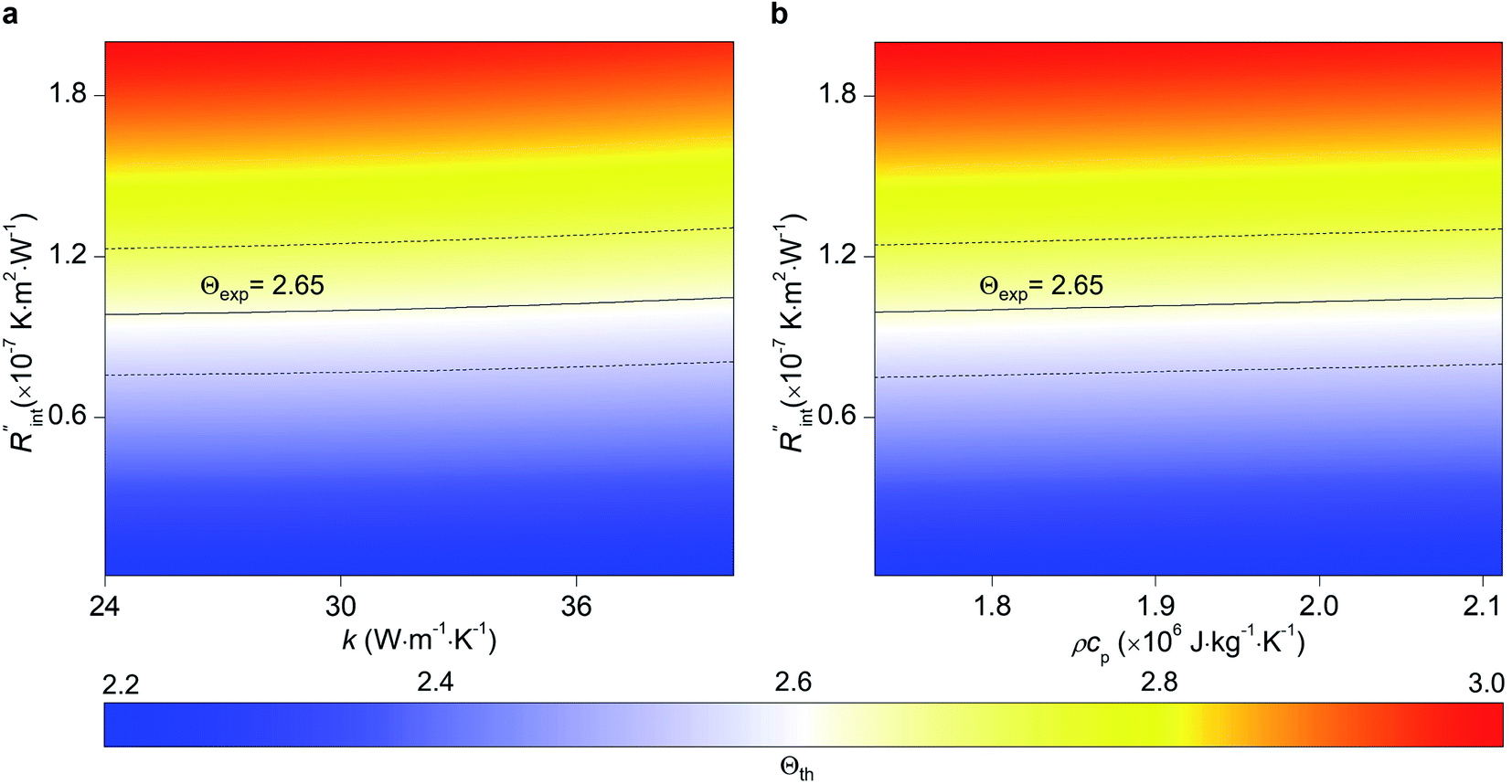 | ||
Fig. 5 Effects of (a) in-plane thermal conductivity (k) and (b) volumetric heat capacity (ρcp) of WS2 thin film on measured  in this work. Each contour shows the calculated Θth for a range of k and ρcp of Sample 3, and the solid black line indicates the Θexp of this sample corresponding to Table 3. The two dashed lines on each figure are related to the uncertainty in measured in this work. Each contour shows the calculated Θth for a range of k and ρcp of Sample 3, and the solid black line indicates the Θexp of this sample corresponding to Table 3. The two dashed lines on each figure are related to the uncertainty in measured  caused by uncertainty in Θexp. Both plots validate the idea that each of these parameters has a negligible effect on the measured caused by uncertainty in Θexp. Both plots validate the idea that each of these parameters has a negligible effect on the measured  and and  in the nET-Raman method. in the nET-Raman method. | ||
As shown in Fig. 1 and 2(c), we can see that the suspended film is slightly concave toward the hole. In all the aforementioned theoretical calculations that are used to determine  it is assumed that the suspended sample over the hole is completely flat. To check the uncertainty caused by this assumption, a more realistic case is considered. Here, we assume that the center of the sample is concaved 1.5 μm inward, which is an exaggerated case. The new length of the sample (larc) which is the length of the WS2 arc over the hole is ∼10.6 μm for a 10 μm hole. This value is used in our theoretical calculation to find the corresponding interface resistance. Fig. 6(b) shows the results of this study. The measured
  with similar Θexp for Sample 3 (Table 3) is ∼1.1 × 10⁻⁷ m2 K W−1. The uncertainty caused by this elongation in
  is ∼7% (Table 4). Therefore, this film elongation has a negligible effect on the determined
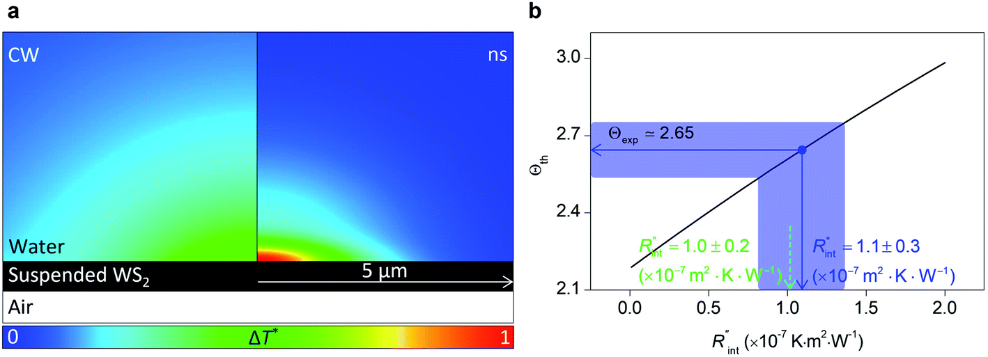 | ||
Fig. 6 (a) Normalized local temperature rise under CW (left contour) and ns (right contour) cases. These contours show that the local temperature rise at the edge of the suspended area, especially in the ns case, is almost zero. And the area under the laser spot contributes most to the Raman weighted average temperature rise that is used in nET-Raman to find interfacial thermal conductance. (b) Determined  using the assumption that the suspended sample is not totally flat and is concave inward 1.5 μm toward the bottom of the hole. Under this situation, the heating area domain and r0 under both states are altered, and updated values are used in the 3D numerical calculation to find using the assumption that the suspended sample is not totally flat and is concave inward 1.5 μm toward the bottom of the hole. Under this situation, the heating area domain and r0 under both states are altered, and updated values are used in the 3D numerical calculation to find  for Sample 3. The green dashed arrow in this plot shows the measured for Sample 3. The green dashed arrow in this plot shows the measured  for flat WS2 film, as reported in Table 4. The error caused by this change in the sample diameter on measured for flat WS2 film, as reported in Table 4. The error caused by this change in the sample diameter on measured  is less than 8%. is less than 8%. | ||
The temperature rise of water at each point in the close vicinity of the WS2 film is calculated and plotted in Fig. 6(a), for both CW and ns cases. Here the normalized local temperature rise (ΔT*) is reported. To find ΔT* at each point, the local temperature rise at that point (ΔT) is divided by the maximum local temperature rise under ns laser heating (ΔTns). This plot shows that ΔT* is mostly increased under the laser spot area, and at higher radii close to the boundaries of the suspended region it is a minimum, and in the case of the ns heating state it is almost zero. This further proves the fact that a minimal increase in the sample length will not affect the Raman weighted average temperature rise of the sample, since the thermal transport mostly occurs under the heating region and not in further away areas.
As mentioned in the main text of the paper, the sensitivity of our technique is mostly controlled by the ns state. The contributions of the thermal resistance of water (Rw) and interfacial resistance (Rint) under this state were elaborated in Section 2.2. The ratio of these two values could be written as:  where kw, αw, and t0 are the thermal conductivity and thermal diffusivity of water and laser pulse width.
  represents the thermal diffusivity length in water during laser pulse heating. Therefore, the interfacial thermal conductance (Gint) could be written as:
 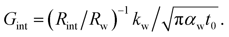 Assuming that a sensible ratio of these two thermal resistance values is 10% and the laser pulse width is short and is in the order of 5 ns, the upper limit of measurable Gint would be around 130 MW m−2 K−1. Also, for similar t0, the upper limit of measurable Gint when the sensible Rint/Rw is 5% will be around 260 MW m−2 K−1.
4. Conclusion
In this work, for the first time, the thermal conductance (Gint) at a liquid–2D material interface was characterized using a novel nET-Raman technique. Two heating states, steady and transient, were introduced to perform the Raman thermometry. Each WS2 film was suspended on a micron-sized hole on a Si substrate and this stage was placed inside a glass container filled with DI water. It was reported that Gint is in the order of ∼10 MW m−2 K−1 for three measured samples and this was compared and verified with other theoretical and experimental works. It was shown that the surface wettability has a significant effect on the interface thermal conductance. A lower contact angle will lead to significantly increased interface thermal conductance. The nET-Raman technique eliminates the effects of laser absorption coefficient and Raman temperature coefficient on the measured parameters. Also, it was shown that any uncertainty caused by uncertainties in thermal properties from reference values has negligible effects on our characterization. Our rigorous calculation showed that shorter ns laser pulses will significantly increase the effect of interface thermal conductance and improve the measurement uncertainty.Conflicts of interest
The authors declare no competing financial interest.Acknowledgements
Support of this work by National Science Foundation (CBET1930866 and CMMI2032464 for X. W.), Program for Professor of Special Appointment (Eastern Scholar) at Shanghai Institutions of Higher Learning, and China Scholarship Council (S. X.) is gratefully acknowledged.References
- S. J. Reed and I. Mudawar, Int. J. Heat Mass Transfer, 1997, 40, 2379–2392 CrossRef CAS.
- H. Han, C. Schlawitschek, N. Katyal, P. Stephan, T. Gambaryan-Roisman, F. d. r. Leroy and F. Müller-Plathe, Langmuir, 2017, 33, 5336–5343 CrossRef CAS.
- X. J. Zhao, G. Zhu, Y. J. Fan, H. Y. Li and Z. L. Wang, ACS Nano, 2015, 9, 7671–7677 CrossRef CAS.
- S. Murad and I. K. Puri, J. Chem. Phys., 2012, 137, 081101 CrossRef.
- Z. Ahmadi, B. Yakupoglu, N. Azam, S. Elafandi and M. Mahjouri-Samani, Int. J. Extreme Manuf., 2019, 1, 015001 CrossRef CAS.
- D. Pal and Y. K. Joshi, J. Thermophys. Heat Transfer, 1998, 12, 256–262 CrossRef CAS.
- K. Cvecek, S. Dehmel, I. Miyamoto and M. Schmidt, Int. J. Extreme Manuf., 2019, 1, 042001 CrossRef CAS.
- D. Zhang, B. Ranjan, T. Tanaka and K. Sugioka, Int. J. Extreme Manuf., 2020, 2, 015001 CrossRef CAS.
- B. Ramos-Alvarado, S. Kumar and G. Peterson, J. Phys. Chem. Lett., 2016, 7, 3497–3501 CrossRef CAS.
- S. Lal, S. E. Clare and N. J. Halas, Acc. Chem. Res., 2008, 41, 1842–1851 CrossRef CAS.
- O. Neumann, A. S. Urban, J. Day, S. Lal, P. Nordlander and N. J. Halas, ACS Nano, 2013, 7, 42–49 CrossRef CAS.
- J. Gao, R. Zheng, H. Ohtani, D. Zhu and G. Chen, Nano Lett., 2009, 9, 4128–4132 CrossRef CAS.
- R. Prasher, P. E. Phelan and P. Bhattacharya, Nano Lett., 2006, 6, 1529–1534 CrossRef CAS.
- D. G. Cahill, W. K. Ford, K. E. Goodson, G. D. Mahan, A. Majumdar, H. J. Maris, R. Merlin and S. R. Phillpot, J. Appl. Phys., 2003, 93, 793–818 CrossRef CAS.
- G. L. Pollack, Rev. Mod. Phys., 1969, 41, 48 CrossRef CAS.
- Z. Shi, M. Barisik and A. Beskok, Int. J. Therm. Sci., 2012, 59, 29–37 CrossRef CAS.
- R. S. Prasher and P. E. Phelan, J. Heat Transfer, 2001, 123, 105–112 CrossRef CAS.
- J.-L. Barrat and F. Chiaruttini, Mol. Phys., 2003, 101, 1605–1610 CrossRef CAS.
- B. H. Kim, A. Beskok and T. Cagin, J. Chem. Phys., 2008, 129, 174701 CrossRef.
- A. Giri, J. L. Braun and P. E. Hopkins, J. Phys. Chem. C, 2016, 120, 24847–24856 CrossRef CAS.
- T. Q. Vo and B. Kim, Int. J. Precis. Eng. Manuf., 2015, 16, 1341–1346 CrossRef.
- G. Balasubramanian, S. Banerjee and I. K. Puri, J. Appl. Phys., 2008, 104, 064306 CrossRef.
- S. Murad and I. K. Puri, Appl. Phys. Lett., 2008, 92, 133105 CrossRef.
- N. Shenogina, R. Godawat, P. Keblinski and S. Garde, Phys. Rev. Lett., 2009, 102, 156101 CrossRef.
- M. Barisik and A. Beskok, J. Comput. Phys., 2012, 231, 7881–7892 CrossRef CAS.
- M. Barisik and A. Beskok, Int. J. Therm. Sci., 2014, 77, 47–54 CrossRef CAS.
- A. Pham, M. Barisik and B. Kim, J. Chem. Phys., 2013, 139, 244702 CrossRef.
- H. Han, S. Mérabia and F. Müller-Plathe, J. Phys. Chem. Lett., 2017, 8, 1946–1951 CrossRef CAS.
- A. R. Bin Saleman, H. K. Chilukoti, G. Kikugawa, M. Shibahara and T. Ohara, Int. J. Heat Mass Transfer, 2017, 105, 168–179 CrossRef CAS.
- O. M. Wilson, X. Hu, D. G. Cahill and P. V. Braun, Phys. Rev. B: Condens. Matter Mater. Phys., 2002, 66, 224301 CrossRef.
- Z. Ge, D. G. Cahill and P. V. Braun, J. Phys. Chem. B, 2004, 108, 18870–18875 CrossRef CAS.
- Z. Ge, D. G. Cahill and P. V. Braun, Phys. Rev. Lett., 2006, 96, 186101 CrossRef.
- J. Park, J. Huang, W. Wang, C. J. Murphy and D. G. Cahill, J. Phys. Chem. C, 2012, 116, 26335–26341 CrossRef CAS.
- J. Park and D. G. Cahill, J. Phys. Chem. C, 2016, 120, 2814–2821 CrossRef CAS.
- H. Malekpour and A. A. Balandin, J. Raman Spectrosc., 2018, 49, 106–120 CrossRef CAS.
- J.-U. Lee, D. Yoon, H. Kim, S. W. Lee and H. Cheong, Phys. Rev. B: Condens. Matter Mater. Phys., 2011, 83, 081419 CrossRef.
- R. Wang, H. Zobeiri, H. Lin, W. Qu, X. Bai, C. Deng and X. Wang, Carbon, 2019, 147, 58–69 CrossRef CAS.
- S. Sahoo, A. P. Gaur, M. Ahmadi, M. J.-F. Guinel and R. S. Katiyar, J. Phys. Chem. C, 2013, 117, 9042–9047 CrossRef CAS.
- N. Peimyoo, J. Shang, W. Yang, Y. Wang, C. Cong and T. Yu, Nano Res., 2015, 8, 1210–1221 CrossRef CAS.
- R. Wang, H. Zobeiri, Y. Xie, X. Wang, X. Zhang and Y. Yue, Adv. Sci., 2020, 2000097 CrossRef CAS.
- P. Yuan, C. Li, S. Xu, J. Liu and X. Wang, Acta Mater., 2017, 122, 152–165 CrossRef CAS.
- P. Yuan, R. Wang, H. Tan, T. Wang and X. Wang, ACS Photonics, 2017, 4, 3115–3129 CrossRef CAS.
- P. Yuan, R. Wang, T. Wang, X. Wang and Y. Xie, Phys. Chem. Chem. Phys., 2018, 20, 25752–25761 RSC.
- P. Yuan, H. Tan, R. Wang, T. Wang and X. Wang, RSC Adv., 2018, 8, 12767–12778 RSC.
- R. Wang, T. Wang, H. Zobeiri, P. Yuan, C. Deng, Y. Yue, S. Xu and X. Wang, Nanoscale, 2018, 10, 23087–23102 RSC.
- H. Zobeiri, R. Wang, T. Wang, H. Lin, C. Deng and X. Wang, Int. J. Heat Mass Transfer, 2019, 133, 1074–1085 CrossRef CAS.
- P. O'hare, W. Hubbard, G. Johnson and H. Flotow, J. Chem. Therm., 1984, 16, 45–59 CrossRef.
- H. Zobeiri, R. Wang, Q. Zhang, G. Zhu and X. Wang, Acta Mater., 2019, 175, 222–237 CrossRef CAS.
- H.-L. Liu, C.-C. Shen, S.-H. Su, C.-L. Hsu, M.-Y. Li and L.-J. Li, Appl. Phys. Lett., 2014, 105, 201905 CrossRef.
- S. Alfihed, M. Hossain, A. Alharbi, A. Alyamani and F. H. Alharbi, J. Mater., 2013, 2013 Search PubMed.
- J. He, D. He, Y. Wang, Q. Cui, F. Ceballos and H. Zhao, Nanoscale, 2015, 7, 9526–9531 RSC.
- P. Yuan, J. Liu, R. Wang and X. Wang, Nanoscale, 2017, 9, 6808–6820 RSC.
- P. Jiang, X. Qian, X. Gu and R. Yang, Adv. Mater., 2017, 29, 1701068 CrossRef.
- S. Sinha, V. Sathe and S. K. Arora, Solid State Commun., 2019, 298, 113626 CrossRef CAS.
- H. Zobeiri, R. Wang, C. Deng, Q. Zhang and X. Wang, J. Phys. Chem. C, 2019, 123, 23236–23245 CrossRef CAS.
- H. Zobeiri, S. Xu, Y. Yue, Q. Zhang, Y. Xie and X. Wang, Nanoscale, 2020, 12, 6064–6078 RSC.
- Y.-Y. Chen, M. Gholipour and D. Chen, 2016 21st Asia and South Pacific Design Automation Conference (ASP-DAC), IEEE, 2016, 761–768 Search PubMed.
- A. N. Gandi and U. Schwingenschlögl, Chem. Mater., 2014, 26, 6628–6637 CrossRef CAS.
- Z. Luo, J. Maassen, Y. Deng, Y. Du, R. P. Garrelts, M. S. Lundstrom, D. Y. Peide and X. Xu, Nat. Commun., 2015, 6, 1–8 Search PubMed.
- M. T. Pettes, J. Maassen, I. Jo, M. S. Lundstrom and L. Shi, Nano Lett., 2013, 13, 5316–5322 CrossRef CAS.
- J. Cognard, Gold Bull., 1984, 17, 131–139 CrossRef CAS.
- K. L. Osborne III, Masters Theses, Worcester Polytechnic Institute, 2009.
- T. Smith, J. Colloid Interface Sci., 1980, 75, 51–55 CrossRef CAS.
- J. Gardner and R. Woods, J. Electroanal. Chem. Interfacial Electrochem., 1977, 81, 285–290 CrossRef CAS.
- L. Preethi, R. P. Antony, T. Mathews, S. Dash and A. Tyagi, J. Nanosci. Nanotechnol., 2016, 16, 10087–10096 CrossRef CAS.
- P. K. Chow, E. Singh, B. C. Viana, J. Gao, J. Luo, J. Li, Z. Lin, A. L. Elias, Y. Shi and Z. Wang, ACS Nano, 2015, 9, 3023–3031 CrossRef CAS.
- B. K. Choi, I. H. Lee, J. Kim and Y. J. Chang, Nanoscale Res. Lett., 2017, 12, 1–6 CrossRef.
Footnotes |
| † Electronic supplementary information (ESI) available. See DOI: 10.1039/d0na00844c |
| ‡ H. Zobeiri, N. Hunter, and R. Wang contributed equally to this work. |
| This journal is © The Royal Society of Chemistry 2020 |