
 Open Access Article
 This Open Access Article is licensed under a Creative Commons Attribution-Non Commercial 3.0 Unported Licence
Room-temperature random lasing of metal-halide perovskites via morphology-controlled synthesis†
Yu-Heng
Hong
 and
Tsung Sheng
Kao
*
and
Tsung Sheng
Kao
*
Department of Photonics and Institute of Electro-Optical Engineering, College of Electrical and Computer Engineering, National Chiao Tung University, Hsinchu 30050, Taiwan. E-mail: tskao@nctu.edu.tw
First published on 31st October 2020
Abstract
Film morphology and the corresponding structural configuration can profoundly affect the optical performance, especially the random lasing action in organic–inorganic metal-halide perovskite thin films. They can be controlled in both micro- and nano-scale by manipulating different processing parameters such as the ratios of engineered solvent mixtures, spin-coating speed and backplane temperature. With the optimized parameters, the synthesized bare perovskite thin films can achieve room-temperature random lasing action with the energy pumping threshold down to 0.9 mJ cm−2 and the corresponding β factor is estimated to be about 0.14. The bare films also show a long-time lasing reliability, maintaining lasing intensity after an optical pumping of 12 × 105 pulses. Meanwhile, in the lifetime test under ambient conditions, the bare films can sustain up to 7 days without any sealing package. Moreover, the perovskite thin films can also be synthesized on flexible substrates with the total area up to 100 cm2, paving a potential way for fabricating large-area and flexible random lasers in speckle-free laser projection and imaging.
1. Introduction
Organic–inorganic metal-halide perovskite composites exhibit significant properties such as a long carrier diffusion length1–4 and a high tolerance of structural defects.5,6 With these advantageous properties, organic–inorganic perovskite composites provide captivating prospects in photovoltaic devices7–9 with a certified photoelectric conversion efficiency (PCE) up to 25.2%.10 Furthermore, with the perovskite-based tandem technology, monolithic perovskite/silicon tandem solar cells can have noteworthy improvement on the PCE and the recently certified record PCE can even achieve 29.1%.10 In addition to their remarkable success in photovoltaic devices, organic–inorganic perovskite composites are also rapidly developed as the emerging light sources, such as light-emitting diodes11–16 and lasers.17–20 Moreover, organic–inorganic perovskite composites can be easily and chemically substituted during the solution-processable fabrication due to their tunable elemental composition, realizing a broad wavelength tunability across the entire visible spectrum.17,21 Solution-processed fabrication and the extensive wavelength tunability make organic–inorganic perovskites quite suited for manufacturing cost-effective and large-area optoelectronic devices.However, the material quality and even the reliability in the ambient environment are challenges facing the urgent need to solve. Several strategies have been adopted, such as fast laser crystallization for achieving highly crystalline structures and uniform film morphology,22 covering an additional graphene layer on the top for improving the air-stability,23 adding caffeine as an extra additive for improving the performance and the thermal stability24 and changing all organic components to inorganic components for preventing the degradation by ultraviolet light.25 These strategies are often incompatible with the currently existing process or need additional steps and extra optimization for fabricating appropriate devices.
Among these strategies and fabrication methods for synthesizing high-quality perovskite thin films, the spin-coating process is a promising solution-processing method for fabricating low-cost and large-area thin-film optoelectronic devices. Therefore, several fabrication processes based on spin-coating strategies have been proposed and demonstrated. Sequentially deposited perovskite thin films in the conventional two-step spin-coating process are composed of large polycrystalline grains and the surface morphology is inhomogeneous with lots of air-voids.26 The poor surface morphology and roughness are due to the high boiling point, up to 153 °C, of N,N-dimethylformamide (DMF) and will give rise to slow crystallization during the spin-coating process, which may suppress the performance of fabricated devices.
Consequently, to regulate the perovskite crystallization process, in 2014, Xiao et al. first introduced the one-step fast deposition-crystallization method to achieve highly uniform perovskite thin films with full surface convergence.27 By adopting an anti-solvent dripping technique during the spin-coating process, the material crystallization can be controlled and the solvent-induced aggregation of perovskites can internally generate numerous polycrystalline grains, forming a smooth surface morphology.
Apart from the anti-solvent dripping technique, the perovskite crystallization process can also be controlled by the selection of the precursor solution. In 2014, Jeon et al. revealed the formation of an intermediate phase, a Lewis acid-base adduct, in the as-prepared perovskite thin film while using a solvent mixture of dimethyl sulfoxide (DMSO) and γ-butyrolactone (GBL) for preparing the precursor solution.28,29 It was found that the intermediate phase formed in the solution-processed synthesis of perovskite thin films can deeply promote the quality of film morphology. Therefore, from then on, the anti-solvent dripping technique along with the precursor solution dissolved in different solvent mixtures, so-called solvent engineering, has been extensively adopted as a simple and promising strategy to fabricate compact and high-quality perovskite thin films for high-performance photovoltaic devices.30–33
Despite the fact that the selection of solvent mixtures has infinite combinations, previous studies suggested that this specific intermediate phase is quite crucial for synthesizing a desirable film morphology. In 2016, Rong et al. investigated non-stoichiometric intermediate phase transitions during the thermal annealing process.34,35 Later on, in 2017, Bai et al. showed a pure intermediate phase by conducting a systematic study on the different volume ratios of DMSO and DMF.36 Additionally, the decomposition of the perovskite intermediate phase during the annealing process can overall facilitate and substantially increase perovskite crystalline domains.37 Therefore, by strictly manipulating the volume ratio of DMSO in the solvent mixture, the desirable film morphology can be obtained and improved optical performance can be achieved. The anti-solvent dripping technique along with solvent engineering combines the flexibility of the solution-processed spin-coating method with the controllability of the intermediate phase, and thus provides a promising way for low-cost and large-area manufacturing with high-commercial prospects.
For perovskite lasers, miscellaneous strategies and methods had been demonstrated for lasing. Intrinsically, cavities can be accomplished by different polygon shapes, such as whispering gallery modes of polygon-shaped crystalline platelets,38 and Fabry–Perot oscillation of nanowires and pyramid cavities.39,40 Well-controlled and single-crystal configurations with appropriate crystal facets can serve as reflecting mirrors, like the mirrors in a conventional laser cavity. Furthermore, these configurations set records in low pumping thresholds with a high-quality factor of light-emitting performance. On the other hand, perovskite thin films with designed patterns, i.e., integrated with extrinsic cavities are also acceptable. Patterned perovskite thin films, such as a metal-clad distributed feedback Bragg (DFB) resonator using an interference lithography,41 can be utilized for lasing. Nevertheless, the pumping threshold is unfavorable, attributed to the high loss of a substandard surface roughness. Additionally, for a more flattened cavity, perovskite thin films with a thermal nanoimprinting photonic crystal had also been demonstrated, realizing the scalability of thin film lasers to a two-dimensional multi-pixelated array of microlasers.42
However, the mentioned laser resonators for achieving a lasing action need additional steps or different fabrications, such as carefully engineered nanostructures, additional adhesive layer configurations or well-controlled crystal growth. Therefore, they are not cost-effective in mass-production because well-designed cavities are in demand, restricting their practical application. Moreover, they still cannot achieve large-area lasing and sacrifice the flexibility of the solution-processed spin-coating method. In our work, we keep the advantages of the solution process in metal-halide perovskite fabrication and make good use of the inherent scattering in the gain medium without a proposed laser cavity to achieve a random lasing action.
Notwithstanding that amplified spontaneous emission (ASE) from a 2D perovskite thin film was observed by Kondo et al. as early as 1998, the requirements of cryogenic conditions are stumbling blocks for further applications.43 Later on, in 2004, Kondo et al. reported ASE in all-inorganic cesium lead chloride perovskite (CsPbCl3) polycrystalline thin films prepared by amorphous-to-crystalline transformation at low temperature, up to about 180 K.44,45 Forthwith, the same group demonstrated room-temperature ASE in cesium lead chloride and bromide perovskite (CsPbCl3 and CsPbBr3) polycrystalline thin films, in 2005 and 2007, respectively.46,47 However, the complex procedure for fabricating perovskite thin films has severe restrictions. Not until 2014, Xing et al. revealed ASE from organic–inorganic hybrid perovskite thin films in a cavity-free configuration which could provide promising optical gain with great wavelength tunability.17
Accordingly, to attain room-temperature and large-area lasing action, in 2014, Dhanker et al. first reported optically pumped random lasing action in methylammonium lead iodide (MAPbI3) perovskite microcrystal networks using the spin-coating technique.18 In our previous study, we found that random lasing action can be generated from multiple random scattering provided by embedded crystalline nanostructures and random lasing behaviours may be altered upon a temperature-induced phase transition.19 In 2016, Shi et al. performed a comprehensive study on the optical properties of solution-processed MAPbI3 perovskite thin films via temperature-dependent and excitation power-dependent photoluminescence measurements.48 The relationship between light emission properties and phase states at different temperatures was also investigated along with the estimation of exciton binding energy and optical phonon energy. In the same year, we demonstrated a feasible tunability of perovskite morphology with different nanocrystal sizes by manipulating the precursor solution concentration in a two-step sequential deposition process.49 The corresponding excitonic properties and lasing performance indicated a high correlation with the formed morphology of the perovskite nanocrystals. In 2017, Duan et al. revealed that miscellaneous lasing actions in perovskite thin films can also be generated from internal resonances.50 Experimental and numerical verifications provide a further understanding of the lasing action and the corresponding mechanism in such a complex lead halide perovskite system. In 2018, Weng et al. went a step further and demonstrated a frequency-upconverted random lasing from organometallic halide (CH3NH3PbBr3) perovskite thin films via a three-photon absorption process.51 Although these studies take advantage of the solution-processed spin-coating method as a low-cost fabriction method and can achieve large-area random lasing action, the surface morphology of synthesized perovskite thin films is still inhomogeneous with lots of air-voids, which will quickly degrade due to their large surface area without any sealing package.
2. Experimental
2.1 Perovskite thin film fabrication
In this work, we investigate and exploit an optimized fabrication via a solvent engineering process with an anti-solvent dripping technique. We take lasing performance as the first concern for further optimization. In this process, we take GBL and DMSO as the precursors in solution-processed perovskite fabrications. Different volume ratios of solvent mixtures are used to control not only the crystallization rate, but also the structural morphology of grain boundaries in perovskite thin films. First, powdered lead(II) bromide (PbBr2) and methylammonium bromide (MABr) were included in the engineered GBL/DMSO solvent mixture and kept stirring at 60 °C until completely dissolved, turning into a transparent precursor solution of 1 molar concentration (M). Next, the as-prepared precursor solution was deposited onto UV-O3 treated glass substrates by a consecutive spin-coating process at 1000 and 5000 rpm for 10 and 50 seconds, respectively. During the second spin-coating step, anti-solvent toluene along with a delay time of 25 seconds was dripped onto the glass substrates. Finally, the resulting thin films were annealed at 100 °C for 30 minutes to remove the residual solvents and transit the intermediate solvate phase into the perovskites, generating orange and bright lead bromide perovskite thin films. All of the fabrications were conducted in a nitrogen-filled glove box at room temperature.2.2 Film morphology
To investigate the surface morphology and estimate the grain boundary size, scanning electron microscopy (SEM) is conducted for MAPbBr3 perovskite thin films at different volume ratios of GBL and DMSO solvents. From the SEM images and graphic processing, we may estimate the occupation ratios of the existing perovskite nanocrystals. As shown in the extracted results in Fig. 1(a), we may observe more air-voids generated in the synthesized MAPbBr3 perovskite thin films with a higher GBL volume ratio. The synthesized perovskite samples at a higher GBL volume ratio of precursor solution will have a rugged film surface, generating inhomogeneous films and dreadful surface convergence. This is due to the fact that the solubility of powdered PbBr2 and MABr in GBL is low, leading to the low concentration of precursor solution and sparse perovskite thin films. As the volume ratio of DMSO increases, higher surface convergence of thin films can be achieved. The highest surface filling factor is reached at the volume ratio of 6![[thin space (1/6-em)]](https://www.rsc.org/images/entities/char_2009.gif) :4 and the highest surface convergence can be accomplished. The insets of Fig. 1(a) show the optical microscopy (OM) image and the corresponding SEM image of the synthesized MAPbBr3 perovskite thin film at the volume ratio of 7:3. From the OM image, some large micro-scale fractal edges on the film surface can be observed while the overall surface morphology is dense without air-voids. Furthermore, different revolutions per minute (rpm) should also be considered, as shown in Fig. S2(b).† While the rpm is too low, the centrifugal force is not enough to evenly spread the precursor solution, and inhomogeneous films will be generated with lots of air-voids. Meanwhile, if the rpm is too high, the precursor solution will volatilize too fast, and a rugged film surface will be generated with lots of blocky aggregates.
:4 and the highest surface convergence can be accomplished. The insets of Fig. 1(a) show the optical microscopy (OM) image and the corresponding SEM image of the synthesized MAPbBr3 perovskite thin film at the volume ratio of 7:3. From the OM image, some large micro-scale fractal edges on the film surface can be observed while the overall surface morphology is dense without air-voids. Furthermore, different revolutions per minute (rpm) should also be considered, as shown in Fig. S2(b).† While the rpm is too low, the centrifugal force is not enough to evenly spread the precursor solution, and inhomogeneous films will be generated with lots of air-voids. Meanwhile, if the rpm is too high, the precursor solution will volatilize too fast, and a rugged film surface will be generated with lots of blocky aggregates.
 | ||
| Fig. 1 The estimation of top-view and cross-section filling factors for synthesized MAPbBr3 perovskite thin films with precursor mixtures prepared at different volume ratios. (a) The estimation of top-view filling factors from SEM images in the micro-scale. Insets: (i) the top-view OM images of synthesized MAPbBr3 perovskite thin films at the volume ratio of 7:3. (ii) The top-view SEM images of synthesized MAPbBr3 perovskite thin films. The corresponding AFM measurement indicates the root mean square of roughness (Rrms) and average roughness (Ravg) of about 2.06 nm and 1.53 nm, respectively. (b) The estimation of cross-section filling factors from TEM images in the nano-scale. Insets: (i) the cross-sectional TEM images of synthesized MAPbBr3 perovskite thin films at the volume ratio of 7:3. (ii) and (iii) The crystalline structure formation and the corresponding crystal orientation direction. | ||
From the SEM image, tightly arranged perovskite micro-crystalline grains on the surface can be observed and the synthesized thin film consists of compact and interconnected grain boundaries. The surface morphology in the micro-scale and the estimation of top-view filling factors provide a direct way to evaluate the film quality of surface convergence. Moreover, through the measurement by atomic force microscopy, the root mean square of roughness (Rrms) and the average of roughness (Ravg) are found to be about 2.06 nm and 1.53 nm, respectively, confirming that the surface morphology is smooth and homogeneous.
2.3 Structural configurations
To further investigate the crystalline structure configuration of the MAPbBr3 perovskite thin films synthesized at different volume ratios, a transmission electron microscope (TEM) is then employed. As shown in Fig. S3,† the cross-sectional images pf the nano-scale of MAPbBr3 perovskite thin films synthesized at three distinct volume ratios can be observed. Again, with the higher volume ratio of DMSO, denser synthesized MAPbBr3 perovskite thin films can be obtained. The estimated cross-section filling factors at three distinct volume ratios are shown in Fig. 1(b). The cross-section filling factor increases as the volume ratio of DMSO increases. And the cross-section filling factor reaches 89% at the volume ratio of 6:4. The insets of Fig. 1(b) show the cross-sectional TEM image and the corresponding crystalline structure formation of the synthesized MAPbBr3 perovskite thin film at the volume ratio of 7:3. Abundant nanocrystalline grains in the synthesized MAPbBr3 perovskite can be observed from the cross-sectional TEM view. The inclusions of dark black aggregates and the white hollows represent the nanocrystalline grains and the un-crystallized air-holes, respectively. By taking fast Fourier transform, the diffraction pattern with clear and sharp peaks indicates that the nanocrystalline structures grew in the orientation direction of (111) and indeed confirms the existence of single nanocrystalline structures in the synthesized perovskites. The cross-sectional TEM images and the estimation of cross-section filling factors in the nano-scale provide a deep insight into the crystalline structure formation of MAPbBr3 perovskite thin films synthesized at different volume ratios, and therefore we can estimate the crystallinity of the synthesized perovskites.
3. Results and discussion
3.1 Random lasing performance
The light emission performance of various MAPbBr3 perovskite samples synthesized at different volume ratios of the engineered solvent is examined by a series of power-dependent photoluminescence (PL) measurements at room temperature. The power-dependent PL emission spectra of synthesized MAPbBr3 perovskite samples are obtained using a 355 nm third-harmonic generation (THG) Nd:YVO4 pulsed laser as an optical pumping source with the pulse duration and the repetition rate of 0.5 ns and 1 kHz, respectively.In this work, we aim to obtain the optimized random lasing action in perovskite thin films. The random lasing behaviour in solution-processed perovskite thin films results from the efficient random scattering in the composed perovskite nanocrystals. Therefore, the filling ratio of the synthesized perovskite nanocrystals and grain boundaries may be one of the key factors to obtain the optimized random lasing action in perovskite thin films. In the fabrication process, we considered and controlled several synthesis parameters such as the ratios of engineered solvent mixtures and spin-coating speed, to acquire the perovskite thin film with the optimized lasing performance. In our results, we found that the MAPbBr3 perovskite thin films synthesized at the engineered solvent volume ratio of 7:3 exhibit a lowest lasing threshold and the highest light-emitting intensity in the lasing mode.
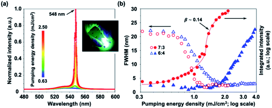
The PL emission spectra of synthesized MAPbBr3 perovskite thin films at the volume ratio of 7:3 are shown in Fig. 2(a). As the optical pumping energy density increases, the emission intensity increases. When the optical pumping energy density exceeds 0.9 mJ cm−2, the lasing action occurs with dramatically increased light-emitting intensity and the suddenly reduced full width at half maximum (FWHM). Unlike conventional laser devices with well- and pre-defined cavities, the FWHM acquired in the lasing action of perovskite thin films originates from the whole spikes in the random lasing mode. In fact, as shown in Fig. 3(b), the bandwidth of each individual peak in the random lasing mode is less than 1 nm. This may result from the different scattering routes occurred simultaneously in the lasing action.
 | ||
| Fig. 2 Lasing characteristics of MAPbBr3 organic–inorganic metal-halide perovskites. (a) Room-temperature power-dependent PL emission spectra of MAPbBr3 perovskite thin films at the volume ratio of 7:3. Inset: the synthesized MAPbBr3 perovskite thin films at the volume ratio of 7:3 can be easily excited by a commercial continuous-wave laser pointer with the center wavelength of 405 ± 10 nm and the max output power less than 100 mW. (b) The light–light curves extracted from the experimental results synthesized at different volume ratios. | ||
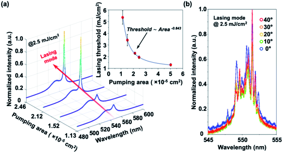 | ||
| Fig. 3 Characterization of perovskite random lasers. (a) Lasing performance controlled by varying different optical pumping areas with fixed optical pumping energy density at 2.5 mJ cm−2. Inset: lasing threshold variation with different optical pumping areas. (b) The ARPL measurements of synthesized MAPbBr3 perovskite thin films at the volume ratio of 7:3. | ||
At the optical pumping energy density of 2 mJ cm−2, the corresponding lasing mode has a spectacularly narrow FWHM down to 2 nm at the centre wavelength of about 548 nm. Besides, as shown in the inset of Fig. 2(a), the synthesized MAPbBr3 perovskite thin film at the volume ratio of 7:3 can be easily excited by a commercial continuous-wave laser pointer with the centre wavelength of 405 ± 10 nm and the maximum output power less than 100 mW. It is worth noting that multiple peaks in the lasing mode occur while the optical pumping energy density is at about 2.5 mJ cm−2. Unlike conventional lasers, there are no specifically defined laser cavities in the synthesized perovskite samples, and the multi-peak lasing action may originate from the random scattering caused by the micro-crystalline grain boundaries or the nanocrystalline grains as the scattering centres in the perovskite thin films.
A comparison of two distinct synthesized MAPbBr3 perovskite samples at different volume ratios that can also achieve room-temperature lasing action is shown in Fig. 2(b). Since the synthesized MAPbBr3 perovskite samples at the volume ratio of 7:3 have the strongest light-emission intensity and the lowest lasing threshold which is down to 0.9 mJ cm−2, fabrication under these conditions is chosen as the optimized solvent-engineered method. Although the synthesized perovskite thin films at the volume ratio of 6:4 can also achieve room-temperature lasing action, it has a higher lasing threshold of about 1.8 mJ cm−2. Meanwhile, the light–light curve of the MAPbBr3 perovskite samples synthesized at the volume ratio of 7:3 shows a clear S-shape, indicating the transition from PL to the lasing regime.
Besides, the β factor is indispensable for a quantitative understanding of gain dynamics and the interaction between lasing action and optical pumping irradiation.52 For a random laser, the lack of directional feedback will restrict the geometric parameters for estimating the β factor, such as the acceptance solid angle of the lasing modes, the mode volume and the frequency in a conventional laser. Thus, the only selection criterion is the spectral dependence of the gain. We calculated the β factor for such a perovskite random laser based on the spectral overlapping of below-threshold spontaneous and above-threshold lasing spectra.53 The corresponding numerical value can be acquired from the experimental PL emission spectra and the corresponding β factor can be estimated to be about 0.14, which is sizeable compared to the conventional semiconductor lasers (β < 10−5). This result is due to the non-directional diffusive feedback of a random laser.
3.2 Random lasing properties
Several characteristics of the random lasing action in the synthesized MAPbBr3 perovskite thin films can be observed. First, while under a high optical pumping energy density, multiple peaks in lasing modes will occur, which is a particular feature different from conventional lasers and may be speculated to be due to the random scattering provided by different sizes of crystalline grains in the synthesized MAPbBr3 perovskite thin films. Second, while the optical pumping energy density increases, the emission spectrum of lasing mode in the synthesized MAPbBr3 thin films will go redder, as shown in Fig. S4†. The emission spectrum of lasing modes at higher optical pumping energy density may originate from the scattering re-absorption of the blue part of the spectrum, and thus the light emission of lasing modes, on average, is redder than the reabsorbed light. Concurrently, the red-shift emission spectrum of lasing mode in the synthesized MAPbBr3 perovskite thin films is also observed compared to the PL mode. The red-shift emission spectrum of lasing mode in the MAPbBr3 thin films comes from the lower absorption loss at the energy tail of spectra.54To get insight into the feasible mechanism and the properties of random lasing action, we first examine the relationship between the lasing threshold and the pumping area. For a random laser, the lasing threshold can be regulated by the optical pumping area. The spreading and the penetration of optical pumping irradiation into such a system will affect the spatial distribution of gain, thus determining the total gain volume. Consequently, the corresponding path length through the gain volume will involve the amplification process. Assuming that the synthesized perovskite thin films are homogeneously scattered samples with even thickness, it was found that the cylindrical gain volume is proportional to the optical pumping area. The larger the pumping area, the larger the corresponding gain volume, and vice versa. In other words, photons can travel in a relatively long path inside the gain volume with a large pumping area. Hence, forming a closed-loop path is effortless and the probability of returning back to the pumping region while reaching the un-pumped edge is larger, resulting in a lower lasing threshold.55
By varying different optical pumping areas, the corresponding changes of the lasing threshold and the numbers of the lasing peak can be controlled. While the optical pumping area increases, the lasing threshold will first decrease and then flat saturate, as shown in the inset of Fig. 3(a). On the other hand, the lasing threshold will increase as the optical pumping area becomes smaller and smaller. The rapid increment of the lasing threshold is because the scattering room provided by the random scattering effect gets smaller, therefore decreasing the closed-loop path in the synthesized MAPbBr3 perovskite thin films. When the optical pumping area is down to 1 × 10⁻⁵ cm2, the random lasing action will no longer happen no matter how large the optical pumping energy density applied. Since the scattering room is not enough for photons to form a closed-loop path, the lasing phenomena will not occur. When the optical pumping area is expanded to 5 × 10⁻⁵ cm2, the flat saturation will happen. After the flat saturation happened, the lasing threshold may be almost independent of the optical pumping area. In this pumping situation, the pumping area may be larger than the effective length of the scattering closed-loop path and the relationship between the lasing threshold and the pumping area is unapparent.
In addition to the pumping-area-related lasing threshold, manipulating different sizes of pumping areas with a fixed optical pumping energy density of 2.5 mJ cm−2 may also control the numbers of the lasing peak, as shown in Fig. 3(a). When the optical pumping energy density is fixed at 2.5 mJ cm−2 with an optical pumping area larger than 2 × 10⁻⁵ cm2, the optical pumping energy density is above the lasing threshold and random lasing action indeed occurs. The random lasing action appears with multiple peaks at the optical pumping area of about 2.46 × 10⁻⁵ cm2. While the optical pumping area is down to about 2.12 × 10⁻⁵ cm2, quasi-single lasing action happens. Different sizes of optical pumping areas can control the scattering room for photons to form a closed-loop path. With a larger optical pumping area, the effective length of the scattering closed-loop path is much longer and multiple peaks in lasing modes will occur. While the optical pumping area gets smaller, the effective length of the scattering closed-loop path decreases, and as a result, quasi-single lasing action happens. Finally, if the optical pumping area is eventually down to 2 × 10⁻⁵ cm2, there is not enough room for photons to form a closed-loop path and no random lasing action will happen.
Another specific feature of a random laser, which is quite different from conventional lasers, is that lasing light irradiation can be detected regardless of detection angles. The angle-resolved PL (ARPL) measurement is then carried out with the same 355 nm THG Nd:YVO4 pulse laser in PL measurements. The detection angle of ARPL is 0 to 40° wide and herein 0° is defined as the normal direction to the sample surface. The synthesized MAPbBr3 perovskite samples are irradiated under the optical pumping energy density of 2.5 mJ cm−2 which is above the lasing threshold. As shown in Fig. 3(b), multiple peaks in lasing modes maintain almost the same spectral profiles and light-emission intensity 0 to 40° wide. The wide-angle detectability of lasing modes in the synthesized MAPbBr3 perovskite samples may imply the contribution of random scattering rather than the predefined cavity in conventional lasers.
3.3 Generalization
After a large number of investigations and optimizations, we try to generalize the same method of solvent engineering along with an anti-solvent dripping technique to synthesize MAPbI3 perovskites. As shown in Fig. 4(a), a series of power-dependent PL emission spectra of synthesized MAPbI3 perovskite thin films is recorded at room temperature. With the higher and higher optical pumping energy density, the intensity of broad spontaneous emission modes increases. While the optical pumping energy density exceeds 0.9 mJ cm−2, the random lasing action indeed occurs at 782 nm with a dramatically increased light-emitting intensity. The corresponding L–L curves extracted from the experimental results of PL measurements are shown in Fig. 4(b). At low optical pumping energy density, the broad spontaneous emission modes have a FWHM of about 35 nm. After the optical pumping energy density exceeds the lasing threshold, which is 0.9 mJ cm−2, the FWHM eventually shrinks down to 7 nm. The results show that the synthesized MAPbI3 perovskite thin films can also achieve room-temperature random lasing action via the identical fabrication of solvent engineering with a clearly S-shaped curve and the corresponding β factor is estimated to be about 0.14. | ||
| Fig. 4 Lasing characteristics of solvent-engineered MAPbI3 perovskite thin films. (a) Power-dependent PL emission spectra of synthesized MAPbI3 perovskite thin films at room temperature. Inset: the MAPbI3 perovskite thin films can be deposited on a PET flexible substrate in a large area of up to 100 cm2. (b) The light–light curves extracted from the experimental results of synthesized MAPbI3 perovskite thin films. | ||
Meanwhile, as shown in the inset of Fig. 4(a), to further extend this solution-processed spin-coating method to large-area and flexible light-emitting devices, we deposited and synthesized MAPbI3 perovskite thin films on a polyethylene terephthalate (PET) flexible substrate with an area up to 100 cm2. Via solvent engineering along with an anti-solvent dripping technique, both synthesized MAPbI3 and MAP-bBr3 perovskite thin films on PET substrates exhibit room-temperature random lasing action providing a practicable way for cost-effective and large-scale manufacturing of flexible random lasers.
3.4 Reliability and lifetime testing
At the same time, the lasing reliability test under a series of pulsed pumping and the lifetime test under ambient conditions without any sealing package are both conducted for practical consideration. For the lasing reliability test, the synthesized MAPbBr3 perovskite bare films are excited at a fixed optical pumping energy density of 1.5 mJ cm−2, which is above the lasing threshold. As a result, the synthesized MAPbBr3 bare films can maintain about 50% of lasing intensity after an optical pumping of 12 × 105 pulses, as shown in Fig. S5(a).† The decrement of lasing intensity may originate from the surface damage caused by the heat accumulation of pumping fluence as shown in the inset of Fig. S5(a).†On the other hand, for the lifetime test, due to the compact and homogenous morphology, the synthesized MAPbBr3 perovskite bare films can sustain up to 7 days under ambient conditions without any sealing package. As shown in Fig. S5(b),† the lasing threshold increases by about 67% from 0.9 mJ cm−2 to 1.5 mJ cm−2. Over time, the integrated and homogenous MAPbBr3 perovskite bare films degrade with lots of air-voids and the corresponding OM images of surface degradation are shown in the inset of Fig. S5(b).† The results of lasing reliability and the lifetime test show the long-time lasing reliability of synthesized MAPbBr3 perovskite bare films, confirming their potential for practical applications.
4. Conclusions
In conclusion, a solvent-engineering method for the preparation of high-quality perovskite thin films with lasing performance has been investigated. In the process, the mixing ratio of GBL and DMSO precursors may vary the grain boundaries and the nanocrystalline occupation in the perovskite thin film, thus affecting the random lasing performance. Via a series of systematic fabrications at different precursor ratios and characterization processes of morphology and photoluminescence properties, we determined the optimum amounts of GBL and DMSO. The MAPbBr3 perovskite thin films synthesized under optimum conditions exhibit room-temperature random lasing action with a lasing threshold of 0.9 mJ cm−2. And a series of optical measurements are performed to gain a greater understanding of the feasible mechanism and the properties of random lasing action. This solvent-engineered method can also be generalized to synthesize MAPbI3 perovskite thin films and the resulting thin films can also achieve room-temperature random lasing action. Also, we extend this solution-processed spin-coating method and synthesize perovskite thin films on PET substrates for flexible random lasing applications. The proposed perovskite thin films on PET substrates with the total area up to 100 cm2 can still achieve room-temperature random lasing action. Moreover, the bare perovskite films also show great long-time lasing reliability. For the lasing reliability, the synthesized MAPbBr3 perovskite bare films can maintain 50% lasing intensity even after an optical pumping of 12 × 105 pulses. In the lifetime test, the synthesized MAPbBr3 perovskite bare films can sustain up to 7 days under ambient conditions without any sealing package. These results not only demonstrate the flexibility of this solvent-engineered spin-coating method but also provide a potential way for fabricating large-area and flexible random lasers. Due to the low spatial coherence property56 and the wide-angle detectability of lasing modes, the synthesized perovskite thin films can be further used as speckle-free light sources for application in laser projection and imaging.Conflicts of interest
There are no conflicts to declare.Acknowledgements
We acknowledge the help of Professor T.-C. Lu and Professor F.-C. Chen at National Chiao Tung University for contributing fruitful discussions and technical support. This work was, in part, financially supported by the Research Team of Photonic Technologies and Intelligent Systems at NCTU within the framework of the Higher Education Sprout Project by the Ministry of Education (MOE) in Taiwan and also partially supported by the Ministry of Science and Technology (MOST) under Contract No. MOST 107-2119-M-009-016 and MOST 107-2221-E-009-116-MY3.Notes and references
- S. D. Stranks, G. E. Eperon, G. Grancini, C. Menelaou, M. J. P. Alcocer, T. Leijtens, L. M. Herz, A. Petrozza and H. J. Snaith, Science, 2013, 342, 341–344 CrossRef CAS.
- G. Xing, N. Mathews, S. Sun, S. S. Lim, Y. M. Lam, M. Gratzel, S. Mhaisalkar and T. C. Sum, Science, 2013, 342, 344–347 CrossRef CAS.
- Z. Guo, Y. Wan, M. Yang, J. Snaider, K. Zhu and L. Huang, Science, 2017, 356, 59–62 CrossRef CAS.
- D. Shi, V. Adinolfi, R. Comin, M. Yuan, E. Alarousu, A. Buin, Y. Chen, S. Hoogland, A. Rothenberger, K. Katsiev, Y. Losovyj, X. Zhang, P. A. Dowben, O. F. Mohammed, E. H. Sargent and O. M. Bakr, Science, 2015, 347, 519–522 CrossRef CAS.
- W.-J. Yin, T. Shi and Y. Yan, Appl. Phys. Lett., 2014, 104, 063903 CrossRef.
- K. Miyano, N. Tripathi, M. Yanagida and Y. Shirai, Acc. Chem. Res., 2016, 49, 303–310 CrossRef CAS.
- H. Zhou, Q. Chen, G. Li, S. Luo, T.-B. Song, H.-S. Duan, Z. Hong, J. You, Y. Liu and Y. Yang, Science, 2014, 345, 542–546 CrossRef CAS.
- M. A. Green, A. Ho-Baillie and H. J. Snaith, Nat. Photonics, 2014, 8, 506–514 CrossRef CAS.
- W. S. Yang, B.-W. Park, E. H. Jung, N. J. Jeon, Y. C. Kim, D. U. Lee, S. S. Shin, J. Seo, E. K. Kim, J. H. Noh and S. I. Seok, Science, 2017, 356, 1376–1379 CrossRef CAS.
- NREL, Best Research-Cell Efficiency Chart. https://www.nrel.gov/pv/assets/pdfs/best-research-cell-efficiencies.20200803.pdf, accessed September, 2, 2020 Search PubMed.
- Z.-K. Tan, R. S. Moghaddam, M. L. Lai, P. Docampo, R. Higler, F. Deschler, M. Price, A. Sadhanala, L. M. Pazos, D. Credgington, F. Hanusch, T. Bein, H. J. Snaith and R. H. Friend, Nat. Nanotechnol., 2014, 9, 687–692 CrossRef CAS.
- F. Zhang, H. Zhong, C. Chen, X. Wu, X. Hu, H. Huang, J. Han, B. Zou and Y. Dong, ACS Nano, 2015, 9, 4533–4542 CrossRef CAS.
- S. D. Stranks and H. J. Snaith, Nat. Nanotechnol., 2015, 10, 391–402 CrossRef CAS.
- G. Li, F. W. R. Rivarola, N. J. L. K. Davis, S. Bai, T. C. Jellicoe, F. de la Peña, S. Hou, C. Ducati, F. Gao, R. H. Friend, N. C. Greenham and Z. K. Tan, Adv. Mater., 2016, 28, 3528–3534 CrossRef CAS.
- B. R. Sutherland and E. H. Sargent, Nat. Photonics, 2016, 10, 295–302 CrossRef CAS.
- J. Pan, Y. Shang, J. Yin, M. De Bastiani, W. Peng, I. Dursun, L. Sinatra, A. M. El-Zohry, M. N. Hedhili, A.-H. Emwas, O. F. Mohammed, Z. Ning and O. M. Bakr, J. Am. Chem. Soc., 2018, 140, 562–565 CrossRef CAS.
- G. Xing, N. Mathews, S. S. Lim, N. Yantara, X. Liu, D. Sabba, M. Grätzel, S. Mhaisalkar and T. C. Sum, Nat. Mater., 2014, 13, 476–480 CrossRef CAS.
- R. Dhanker, A. N. Brigeman, A. V. Larsen, R. J. Stewart, J. B. Asbury and N. C. Giebink, Appl. Phys. Lett., 2014, 105, 151112 CrossRef.
- T. S. Kao, Y.-H. Chou, C.-H. Chou, F.-C. Chen and T.-C. Lu, Appl. Phys. Lett., 2014, 105, 231108 CrossRef.
- A. Balena, A. Perulli, M. Fernandez, M. L. De Giorgi, G. Nedelcu, M. V. Kovalenko and M. Anni, J. Phys. Chem. C, 2018, 122, 5813–5819 CrossRef CAS.
- L. Protesescu, S. Yakunin, M. I. Bodnarchuk, F. Krieg, R. Caputo, C. H. Hendon, R. X. Yang, A. Walsh and M. V. Kovalenko, Nano Lett., 2015, 15, 3692–3696 CrossRef CAS.
- T. Jeon, H. M. Jin, S. H. Lee, J. M. Lee, H. I. Park, M. K. Kim, K. J. Lee, B. Shin and S. O. Kim, ACS Nano, 2016, 10, 7907–7914 CrossRef CAS.
- X. Shen, M. Wang, F. Zhou, B. Qiu, L. Cai, Y. Liu, Z. Zheng and Y. Chai, J. Mater. Chem. C, 2018, 6, 8663–8669 RSC.
- R. Wang, J. Xue, L. Meng, J.-W. Lee, Z. Zhao, P. Sun, L. Cai, Y. Huang, Z. Wang, Z.-K. Wang, Y. Duan, J. L. Yang, S. Tan, Y. Yuan, Y. Huang and Y. Yang, Joule, 2019, 3, 1464–1477 CrossRef CAS.
- G. Niu, W. Li, F. Meng, L. Wang, H. Dong and Y. Qiu, J. Mater. Chem. A, 2014, 2, 705–710 RSC.
- J. Burschka, N. Pellet, S. J. Moon, R. Humphry-Baker, P. Gao, M. K. Nazeeruddin and M. Grätzel, Nature, 2013, 499, 316–319 CrossRef CAS.
- M. Xiao, F. Huang, W. Huang, Y. Dkhissi, Y. Zhu, J. Etheridge, A. Gray-Weale, U. Bach, Y.-B. Cheng and L. Spiccia, Angew. Chem., Int. Ed., 2014, 53, 9898–9903 CrossRef CAS.
- N. J. Jeon, J. H. Noh, Y. C. Kim, W. S. Yang, S. Ryu and S. I. Seok, Nat. Mater., 2014, 13, 897–903 CrossRef CAS.
- J. W. Lee, H. S. Kim and N. G. Park, Acc. Chem. Res., 2016, 49, 311–319 CrossRef CAS.
- Y. Li, J. Wang, Y. Yuan, X. Dong and P. Wang, Sustainable Energy Fuels, 2017, 1, 1041–1048 RSC.
- Y. Guo, J. Ma, H. Lei, F. Yao, B. Li, L. Xiong and G. Fang, J. Mater. Chem. A, 2018, 6, 5919–5925 RSC.
- N. Ahn, D. Y. Son, I. H. Jang, K. S. Min, M. Choi and N. G. Park, J. Am. Chem. Soc., 2015, 137, 8696–8699 CrossRef CAS.
- M. Yang, T. Zhang, P. Schulz, Z. Li, G. Li, D. H. Kim, N. Guo, J. J. Berry, K. Zhu and Y. Zhao, Nat. Commun., 2016, 7, 12305 CrossRef CAS.
- Y. Rong, Z. Tang, Y. Zhao, X. Zhong, S. Venkatesan, H. Graham, M. Patton, Y. Jing, A. M. Guloy and Y. Yao, Nanoscale, 2015, 7, 10595–10599 RSC.
- Y. Rong, S. Venkatesan, R. Guo, Y. Wang, J. Bao, W. Li, Z. Fan and Y. Yao, Nanoscale, 2016, 8, 12892–12899 RSC.
- Y. Bai, S. Xiao, C. Hu, T. Zhang, X. Meng, Q. Li, Y. Yang, K. S. Wong, H. Chen and S. Yang, Nano Energy, 2017, 34, 58–68 CrossRef CAS.
- S. Xiao, Y. Bai, X. Meng, T. Zhang, H. Chen, X. Zheng, C. Hu, Y. Qu and S. Yang, Adv. Funct. Mater., 2017, 27, 1604944 CrossRef.
- Q. Zhang, S. T. Ha, X. Liu, T. C. Sum and Q. Xiong, Nano Lett., 2014, 14, 5995–6001 CrossRef CAS.
- H. Zhu, Y. Fu, F. Meng, X. Wu, Z. Gong, Q. Ding, M. V. Gustafsson, M. T. Trinh, S. Jin and X.-Y. Zhu, Nat. Mater., 2015, 14, 636–642 CrossRef CAS.
- Y. Mi, Z. Liu, Q. Shang, X. Niu, J. Shi, S. Zhang, J. Chen, W. Du, Z. Wu, R. Wang, X. Qiu, X. Hu, Q. Zhang, T. Wu and X. Liu, Small, 2018, 14, 1703136 CrossRef.
- Y. Jia, R. S. Kerner, A. J. Grede, A. N. Brigeman, B. P. Rand and N. C. Giebink, Nano Lett., 2016, 16, 4624–4629 CrossRef CAS.
- S. Chen, K. Roh, J. Lee, W. K. Chong, Y. Lu, N. Mathews, T. C. Sum and A. Nurmikko, ACS Nano, 2016, 10, 3959–3967 CrossRef CAS.
- T. Kondo, T. Azuma, T. Yuasa and R. Ito, Solid State Commun., 1998, 105, 253–255 CrossRef CAS.
- S. Kondo, K. Suzuki, T. Saito, H. Asada and H. Nakagawa, Phys. Rev. B: Condens. Matter Mater. Phys., 2004, 70, 205322 CrossRef.
- S. Kondo, K. Suzuki, T. Saito, H. Asada and H. Nakagawa, J. Cryst. Growth, 2005, 282, 94–104 CrossRef CAS.
- S. Kondo, H. Ohsawa, T. Saito, H. Asada and H. Nakagawa, Appl. Phys. Lett., 2005, 87, 131912 CrossRef.
- S. Kondo, K. Takahashi, T. Nakanish, T. Saito, H. Asada and H. Nakagawa, Curr. Appl. Phys., 2007, 7, 1–5 CrossRef.
- Z. F. Shi, X. G. Sun, D. Wu, T. T. Xu, Y. T. Tian, Y. T. Zhang and G. T. Du, J. Mater. Chem. C, 2016, 4, 8373–8379 RSC.
- T. S. Kao, Y. H. Chou, K. B. Hong, J. F. Huang, C. H. Chou, H. C. Kuo and T. C. Lu, Nanoscale, 2016, 8, 18483–18488 RSC.
- Z. Duan, S. Wang, N. Yi, Z. Gu, Y. Gao, Q. Song and S. Xiao, ACS Appl. Mater. Interfaces, 2017, 9, 20711–20718 CrossRef CAS.
- G. Weng, J. Xue, J. Tian, X. Hu, X. Bao, H. Lin and J. Chu, ACS Photonics, 2018, 5, 2951–2959 CrossRef CAS.
- G. van Soest, F. J. Poelwijk, R. Sprik and A. Lagendijk, Phys. Rev. Lett., 2001, 86, 1522–1525 CrossRef CAS.
- G. van Soest and A. Lagendijk, Phys. Rev. E: Stat., Nonlinear, Soft Matter Phys., 2002, 65, 047601 CrossRef.
- H. H. Fang, S. Adjokatse, S. Shao, J. Even and M. A. Loi, Nat. Commun., 2018, 9, 243 CrossRef.
- G. Van Soest, M. Tomita and A. Lagendijk, Opt. Lett., 1999, 24, 306–308 CrossRef CAS.
- Y.-C. Wang, H. Li, Y.-H. Hong, K.-B. Hong, F.-C. Chen, C.-H. Hsu, R.-K. Lee, C. Conti, T. S. Kao and T.-C. Lu, ACS Nano, 2019, 13, 5421–5429 CrossRef CAS.
Footnote |
| † Electronic supplementary information (ESI) available. See DOI: 10.1039/d0na00794c |
| This journal is © The Royal Society of Chemistry 2020 |