DOI:
10.1039/D0NA00451K
(Paper)
Nanoscale Adv., 2020,
2, 5615-5622
Highly qualified InP based QDs through a temperature controlled ZnSe shell coating process and their DFT calculations†
Received
3rd June 2020
, Accepted 14th October 2020
First published on 15th October 2020
Abstract
For QDs used in displays, a narrow emission linewidth and emission peak tuning depending on the morphology of the QDs are the most important factors in order to maximize the range of colors to be represented. CdSe-based QDs are known as the most suitable QDs for displays, but cadmium is a highly toxic and regulated substance for use worldwide; InP-based QDs are the most noteworthy alternative. However, InP-based QDs have a wider linewidth of emission light in the entire visible region compared to CdSe-based QDs. In this work, we use the ZnSe inner shell as a lattice buffer layer between the InGaP core and the ZnS outer shell in the type-I structure, using a heating-up method in which ZnSe precursors were added to a low-temperature core solution and then rapidly raised to a temperature of 270–320 °C. Interestingly, when reacting at high temperatures, the shape of the QDs changes to a tetrahedron, and the FWHM becomes narrower than at low temperature. To understand this phenomenon, we proceeded with transmission electron microscopy (TEM) and powder X-ray diffraction (PXRD) analyses, and a reasonable explanation was provided with DFT calculations.
1. Introduction
Colloidal semiconductor nanocrystals, commonly known as quantum dots (QDs), have been extensively studied in a variety of fields, such as light emission1–4 and light energy harvesting,5–8 owing to their inherent optoelectronic properties. Among them, research on QDs applicable to displays using a narrow emission linewidth and emission peak tuning depending on the size of the QDs is in progress. In particular, CdSe-based core/shell QDs exhibited good optical properties and stability compared with organic dyes.9–11 However, cadmium is a toxic substance and is a regulated substance for use worldwide.12 Therefore, a substitute material is needed. InP-based QDs are the most noteworthy alternative.
However, the optical performance of such InP-based QDs is inferior to that of CdSe-based QDs, especially the wide linewidth of emission light in the entire visible region, which is represented by the full width at half maximum (FWHM). The FWHM of emission light is a vital characteristic in displays, because it affects the color gamut – specifically, a wider color gamut is obtained with a narrower FWHM. However, in the case of InP QDs as the core, the main research has been focused on achieving high efficiency to alternate CdSe in the green and red emission ranges.13–15 In terms of the FWHM aspect, green has a FWHM of approximately 40–45 nm on average, and 36 nm for the narrowest emission.16 Some studies have been conducted to improve the photoluminescence (PL) line narrowing of InP-based QDs. For example, Li et al. controlled the reaction temperature and used new precursors, which resulted in a quantum yield (QY) of 70% and FWHM of 45 nm in the green region.17
However, the method did not have any effects on the red color. As an another effort, a buffer layer between the InP core and ZnS shell was developed and demonstrated the effects. InP/GaP/ZnS core/shell/shell structures that used a GaP buffer layer between the InP core and ZnS shell have been fabricated.18,19 The QDs exhibited an FWHM of 42 nm and QY of 85%; however, narrower emission was impossible through forming a thicker GaP layer. Ramasamy et al. used a ZnSe buffer layer between InP and ZnS; as a result, InP/ZnSe/ZnS core/shell/shell structures were fabricated.20 To coat high-quality ZnSe shells on InP, the addition of ZnSe precursors was finely controlled, and a QY of 50–70% and an FWHM of 38 nm in the green region and 44 nm in the red region were obtained.21
In this study, InGaP/ZnSe/ZnS core/shell/shell QDs were obtained by coating a ZnSe shell on the InGaP core, using a heating-up method in which ZnSe precursors were added to a low-temperature core solution and then rapidly raised to a temperature higher than 300 °C. Thus, tetrahedral-shaped QDs having an FWHM of 37 nm, green emission of 532 nm, and a QY of 85% were obtained. In the experiment, ZnSe with a bandgap of 2.7 eV and a lattice parameter of 5.66 Å played the role of a lattice buffer layer between the core and outer shell in the type-I band offsets.
To understand the phenomenon of highly improved FWHM, temperature controlled experiments were conducted. Then, an analysis technique using transmission electron microscopy (TEM) and powder X-ray diffraction (PXRD) was introduced, and a reasonable explanation with theoretical modeling was provided.
In addition, this method was applied to red-emitting QDs, and the emission FWHM of more than 60 nm was reduced to 40.4 nm. High crystallinity was obtained, and the QY significantly improved to 78%.
2. Results and discussion
2.1 Green-light-emitting InGaP/ZnSe/ZnS
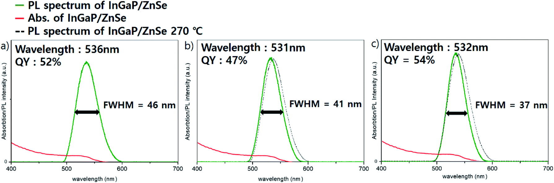
InGaP/ZnSe/ZnS core/shell/shell QDs were fabricated by a slightly modified procedure based on a previous report.18 The experimental details are given in the Experimental section of that work. When TMS-P (tris(trimethylsilyl)phosphine) was injected at various temperatures, the rapid injection at 200 °C showed the best effect on the core synthesis. An absorption peak at about 370 nm is observed after the phosphine injection, (Fig. S1a†), which indicates the formation of the In–P complex known as MSCs (magic sized clusters).22 Then, clear absorption peak shoulder of the InGaP core is observed when heated to 300 °C. The InGaP core has a size of about 2.2–2.5 nm (Fig. S1b†), and shows an absorption peak at about 430 nm. When the ZnS shell without the ZnSe buffer layer is coated on this core, a QY of 85% and a FWHM of 41 nm are observed. The results showed good QY, but a wide FWHM. To improve it, we coated an additional II–VI type ZnSe layer between the core and ZnS shell to release the interfacial stress. Zinc oleate and TOP-Se, used as precursors of the ZnSe shell, were added to the core solution at 200 °C, and the solution was heated to the target temperature and maintained for 1 h. To optimize the optical properties of the QDs, especially the FWHM, the ZnSe shell coating temperature was mainly tuned to 270 °C, 300 °C, and 320 °C, and the effect was impressive. Fig. 1 illustrates the optical properties of the InGaP/ZnSe QDs. The FWHM and the peak of the emission wavelength were 46 nm at a wavelength of 536 nm at 270 °C, 41 nm at 531 nm at 300 °C, and 37 nm at 532 nm at 320 °C. As the temperature increased, the QDs exhibited a narrower FWHM; however, the peaks of the emission wavelength were observed at similar wavelengths regardless of temperature. The QYs of the QDs were also values similar to 50%. The reactions at less than 270 °C (for example, the reaction at 250 °C) exhibited similar results to those at 270 °C. At more than 320 °C, reactions using a high-boiling-temperature solvent (for example, the 340 °C reaction) resulted in aggravated QY and FWHM of QDs.
 |
| | Fig. 1 Absorption and PL data of InGaP/ZnSe with the ZnSe shell coating temperature at (a) 270 °C, (b) 300 °C and (c) 320 °C. | |
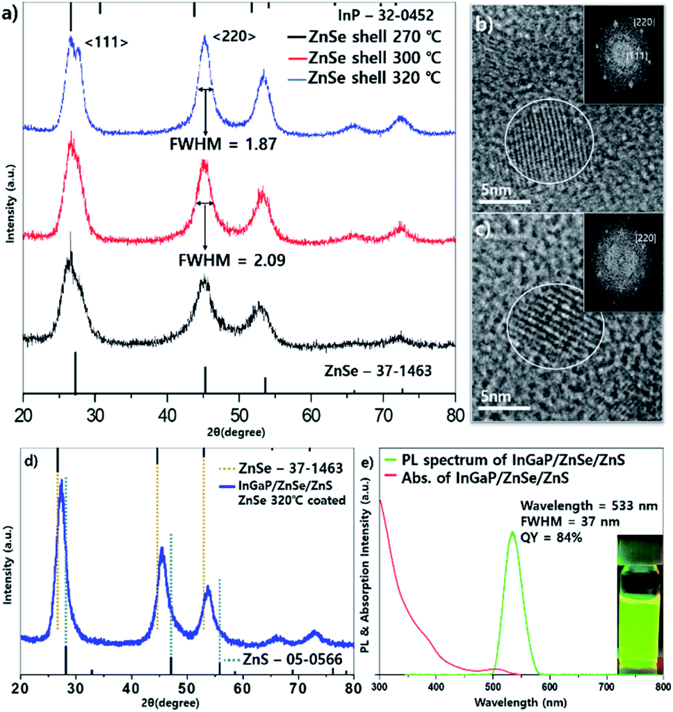
As the temperature of the ZnSe coating increases, why does the FWHM of the emission wavelength become narrower? To answer this question, the particle images and crystal structures were observed using TEM and PXRD. Fig. 2 depicts the low- and high-resolution TEM images according to the temperature, respectively (a and d: 270 °C, b and e: 300 °C, c and f: 320 °C). As depicted in Fig. 2, the higher the temperature, especially when comparing Fig. 2b and c the larger the size of each particle, and the more tetrahedron pot is observed. As the reaction temperature increases, the shape of the QDs became a truncated tetrahedron, which was equally predicted from the DFT calculations (see more details in the theoretical calculation section). Generally, the shape change occurs because of the relative stability of the crystal facet and adsorption/desorption characteristics of the surfactants under high-temperature annealing. When a nanocrystal having a zinc blende structure has a tetrahedral shape, the plane direction of the tetrahedron has 〈111〉 crystal faces. In other words, when the 〈111〉 plane is the most stable, a tetrahedral structure can be formed easily. Kim et al. reported InP QDs of tetrahedral shape with an incredibly developed 〈111〉 facet surface.23 However, PXRD data of samples also indicate the development of a 〈220〉 facet. This can be explained by theoretical calculations.
 |
| | Fig. 2 TEM image of InGaP/ZnSe; (a) and (d) shell coated at 270 °C, (b) and (e) coated at 300 °C, and (c) and (f) coated at 320 °C. | |
The PXRD data showed that every diffraction peak including 〈111〉, 〈220〉, and 〈311〉 became sharpened as the temperature increased (Fig. 3a). The FWHM values of the 〈220〉 peak were 1.87, 2.09, and 2.24 at 320 °C, 300 °C, and 270 °C, respectively, implying that the crystallinity improved as the temperature increased. In the core/shell structure, the diffraction peaks in the X-ray diffraction (XRD) results shifted to the peak of the shell material and were usually located between the core and shell peaks. However, the XRD peaks of the InGaP/ZnSe core/shell were located in the ZnSe position, indicating that the ZnSe shell was very thick. Another characteristic feature is that, as the temperature increased, a 〈220〉 plane developed rather than a 〈111〉 plane. The XRD image demonstrated that the 〈220〉 peak was higher than the 〈111〉 peak. The 〈111〉 peak was split, and the peak of the InP core also appeared. This phenomenon may be attributed to the high crystallinity of the inner core because of annealing at a high temperature during ZnSe shell coating. This also indicates that high-temperature annealing affects not only the ZnSe shell coating, but also the crystallinity of the core itself. The magnified TEM images and their fast Fourier transform (FFT) image also indicate that the high crystallinity was obtained at 320 °C annealing (Fig. 3b and c). The crystalline lattices of the tetrahedron that were annealed at 320 °C were clearly observed compared with those at 300 °C. In the FFT image, a clear hexagonal shape of the 〈220〉 plane was observed in the 320 °C sample; however, the hexagon dots were not clear in the 300 °C sample. From the data, it is known that the crystallinity of the QDs improved, and the FWHM of their PL also narrowed as the temperature of the ZnSe shell coating increased. The QY increased significantly, from 54% to 84% (the best QY was 85%), and the FWHM and emission wavelength did not change (Fig. 3e). The PXRD pattern exhibited a small shift of every peak from ZnSe to ZnS (Fig. 3d), and the particle sizes were a little bigger after the ZnS shell was coated (see the Fig. S2†).
 |
| | Fig. 3 (a) PXRD data of InGaP/ZnSe with the ZnSe shell coating temperature at 270 °C, 300 °C and 320 °C. (b) HR-TEM & live FFT data at 320 °C. (c) HR-TEM & live FFT data at 300 °C. (d) PXRD data of InGaP/ZnSe/ZnS and (e) PL & absorption data of InGaP/ZnSe/ZnS. | |
2.2 Theoretical calculations
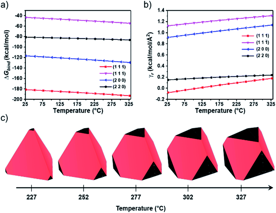
To investigate the relationship between temperature and InGaP/ZnSe QD morphology, density functional theory (DFT) calculations were performed (see Computational details in the Experimental section). Because the volume of the ZnSe shell occupies most of the nanoparticles, the focus is on the surface structure of the ZnSe shell to investigate the morphology of QDs. The low index surfaces with relatively large interplanar distances are likely to be exposed;24–26 thus, the relationship between surface indices and interplanar distances in the ZnSe bulk structure was examined (Table S1†). The slab models representing each surface were stoichiometric, and a vacuum region of approximately 20 Å perpendicular to the surface was applied to avoid self-interaction (Fig. S3†). Because the morphology is largely controlled by the ligand, the interaction of each surface with the ligand is of significant importance.27 DFT calculations were performed considering Zn(oleate)2, because the X-type ligand (i.e.; oleate) can be strongly attached to the ZnSe surface, as in the experiment (Fig. S4†). The interactions between each surface and Zn(oleate)2 were calculated considering the surface with stable termination (Fig. S5†). The detailed lattice parameters of each surface and coverage of Zn(oleate)2 are shown in Table S2.† As shown in Fig. 4a, the Gibbs free energy of the binding of Zn(oleate)2 (ΔGbind) to the (111) surface is the strongest, so the tetrahedral-shaped QDs surrounded by the (111) surface can be observed. Considering the dimerization-anion passivation or co-passivation, the stabilization effect on the cation-terminated (111) surface is higher than that of other surfaces, resulting in a tetrahedral shape.28 To further investigate the morphological change dependence on temperature, we calculated the relaxed surface free energy (γr) (Fig. 4b). The order of stability of the relaxed surface was (111), (220), (200), and (11![[1 with combining macron]](https://www.rsc.org/images/entities/char_0031_0304.gif) ). Interestingly, the (220) surface became the second most stable because of the large contribution of the surface free energy among other energies (Fig. S6†). Additionally, γr(111) and γr(220) became asymptotically close as the temperature increased. Subsequently, the equilibrium morphologies depending on the temperature were calculated through the Wulff construction29 with the γr,’s (Fig. 4c). When the temperature was approximately 227 °C, a tetrahedron predominantly surrounded by a (111) surface was obtained. As the temperature increased further, a (220) surface began to appear at the vertices of the tetrahedron, because the increasing rate of γr(220) was the lowest among the surfaces with considerably low γr(220) (i.e.; in a high-surface-stability state). These morphological changes can affect the change in the XRD peak intensity.30 The increase rate of the 〈220〉 peak intensity in the experimental XRD (Fig. 3a) was found to be greater than that of the 〈111〉 peak intensity because of the increasing areal fraction of the (220) surface in the tetrahedron. It is unclear as to why the FWHM of PL is narrow; however, previous reports can provide guidance. Kim et al. demonstrated that the electrons in the tetrahedron are subject to more quantum confinement than those in the spherical shape of the same volume.23,31 As a result, bandgap changes with size nonuniformity in the tetrahedral-shaped QDs are less than those of spherical QDs. Although the edge lengths are slightly different in the tetrahedral shape, the bandgaps are similar, and the FWHM of the PL become narrower. QDs of the InGaP/ZnSe/ZnS structure were fabricated by adding a zinc-DDT complex as a ZnS precursor.
). Interestingly, the (220) surface became the second most stable because of the large contribution of the surface free energy among other energies (Fig. S6†). Additionally, γr(111) and γr(220) became asymptotically close as the temperature increased. Subsequently, the equilibrium morphologies depending on the temperature were calculated through the Wulff construction29 with the γr,’s (Fig. 4c). When the temperature was approximately 227 °C, a tetrahedron predominantly surrounded by a (111) surface was obtained. As the temperature increased further, a (220) surface began to appear at the vertices of the tetrahedron, because the increasing rate of γr(220) was the lowest among the surfaces with considerably low γr(220) (i.e.; in a high-surface-stability state). These morphological changes can affect the change in the XRD peak intensity.30 The increase rate of the 〈220〉 peak intensity in the experimental XRD (Fig. 3a) was found to be greater than that of the 〈111〉 peak intensity because of the increasing areal fraction of the (220) surface in the tetrahedron. It is unclear as to why the FWHM of PL is narrow; however, previous reports can provide guidance. Kim et al. demonstrated that the electrons in the tetrahedron are subject to more quantum confinement than those in the spherical shape of the same volume.23,31 As a result, bandgap changes with size nonuniformity in the tetrahedral-shaped QDs are less than those of spherical QDs. Although the edge lengths are slightly different in the tetrahedral shape, the bandgaps are similar, and the FWHM of the PL become narrower. QDs of the InGaP/ZnSe/ZnS structure were fabricated by adding a zinc-DDT complex as a ZnS precursor.
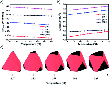 |
| | Fig. 4 (a) Gibbs free energy of binding of Zn(oleate)2 (ΔGbind) to each ZnSe surface; (b) relaxed surface free energy (γr) depending on temperature – ΔGbind is calculated from eqn (1) and (2) and γr is calculated from eqn (8); and (c) equilibrium morphology based on γr with respect to temperature – red and black represent the (111) and (220) surfaces, respectively. | |
2.3 Red-light-emitting InGaP/ZnSe/ZnS
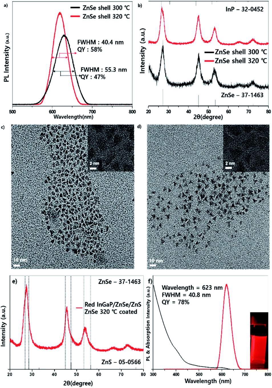
High-temperature-annealing effects were also investigated in red-emitting InP-based QDs. For red-emitting QDs, the core fabrication process was slightly different from that of green-emitting QDs; however, the coating processes for the ZnSe and ZnS shells were the same. The procedure is described in the Experimental section. Fig. 5 shows the PL comparison data of red-emitting QDs, which were fabricated at 300 °C and 320 °C which revealed that the FWHM of PL at 320 °C was 40.4 nm, which was narrower than 55 nm at 300 °C. The QY at 320 °C was 58%, which was also better than 47% at 300 °C (Fig. 5a). The tendency of the FWHM varying with temperature coincided with that of the green-emitting QDs. For the wavelength, the QDs at 300 °C exhibited a longer wavelength of 639 nm compared with 632 nm at 320 °C. It is supposed that the longer wavelength and wide FWHM at 300 °C resulted from bigger sizes and less tetrahedral shapes, respectively. The PXRD data showed that the diffraction peaks at 300 °C and 320 °C are located between the InP and ZnSe references, implying that the shell is not thick compared with the green-emitting QDs (Fig. 5b). TEM images (Fig. 5c and d) demonstrated a more tetrahedral shape at 320 °C, which is similar to those of the green emitting QDs. To increase the QY, additional ZnS shells were coated, the PXRD pattern exhibited a small shift to the ZnS peak (Fig. 5e) and the resulting InGaP/ZnSe/ZnS QDs exhibited a highly improved QY of 78% and a similar emission FWHM of 40.8 nm (Fig. 5f) (the narrowest FWHM is 40.4 nm, and the efficiency at this time is 72%).
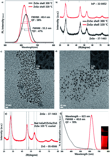 |
| | Fig. 5 (a) PL data of red emitting InGaP/ZnSe QDs with the ZnSe shell coating temperature at 300 °C and 320 °C (b) XRD data, TEM image of (c) 300 °C ZnSe shell coated, (d) 320 °C coated. (e) PXRD data and (f) PL and absorption data of red emitting InGaP/ZnSe/ZnS. | |
2.4 On-chip WLED fabrication
As an application, we fabricated the QD color film with silicon resin. Various resins including POSS, OE-6630 and NR-3170 acrylic resin were tested to form the composite film of the InP-based QD, and the POSS (Polyhedral Oligomeric Silsesquioxane) resin showed the best stability and efficiency among them. We mixed POSS resin with InP QDs in toluene solvent, and the mixture was coated on the slide glass and cured in a 160 °C oven for 2 hours. According to Fig. 6, the green emitting film showed a FWHM of 38.2 nm at a wavelength maximum of 534 nm and the red film showed a FWHM of 41.3 nm at a wavelength maximum of 624 nm (Fig. 6b). From the spectrum data, the CIE (Commission internationale de l'éclairage) coordinates (Cx, Cy) showed (0.2047, 0.7182) for green emission, and (0.6624, 0.3230) for red emission, respectively. When the color gamut is obtained using the InGaN blue LED chip and these coordinates, it is displayed in the region with the NTSC ratio of 105.8% (Fig. 6a). The light efficiency changes according to the time of the on-chip LED made using POSS resin and our QDs were observed (Fig. S7†). They showed that the efficiency was decreased more as the current increased.
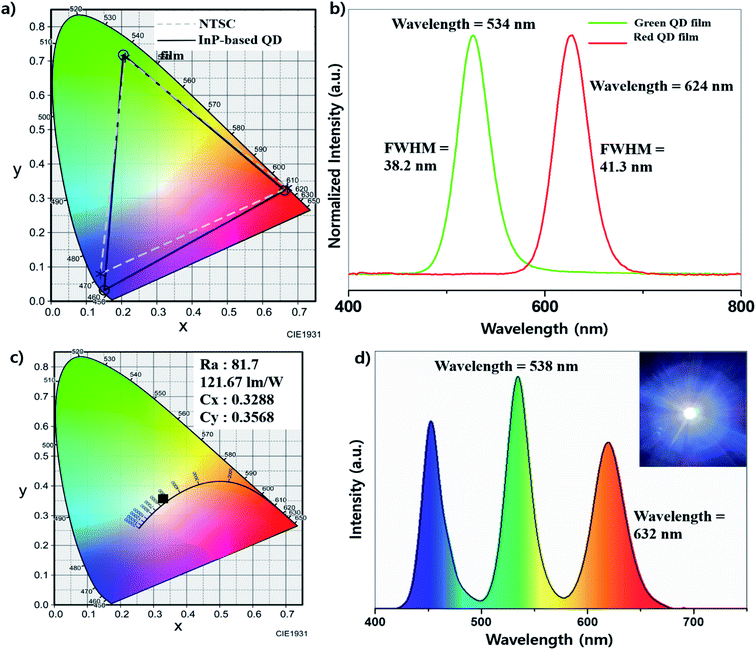 |
| | Fig. 6 (a) CIE 1976 diagram of green and red emitting QD films and the InGaN LED, (b) emission spectrum data of green and red emitting QD films, (c) CIE 1976 diagram of the WLED and (d) emission spectrum data of the WLED from 10 V and 120 mA. | |
From the result of QD film application, we also tried white-light-emitting on-chip LEDs using the InP QDs and InGaN blue LED chip. WLEDs generally use an InGaN blue chip and YAG:Ce (Ce3+–Y3Al5O12) phosphors to implement a white color, but they have a relatively low Ra index due to lack of green and red color ranges.32 Recently, several groups used CdSe-based QDs to improve the green and red regions, and the luminous efficiency and Ra index (90∼) were improved.33,34 We fabricated WLEDs by replacing CdSe-base QDs with InP-based QDs with reference to the above system. QDs and POSS resin are mixed at a weight ratio of 1![[thin space (1/6-em)]](https://www.rsc.org/images/entities/char_2009.gif) :0.24:0.03 (G:R = 8:1 for QD) and the mixture was applied on the LED chip and cured in a 160 °C oven for 2 hours. When processing at 10 V and 120 mA, the luminous efficiency of 118.87 lm w−1 was exhibited. The Cx, Cy values of (0.3288, 0.3568), Ra of 76.7 and CCT of 5652 K were measured (Fig. 6c). The emission spectrum in Fig. 6d shows that the wavelengths are red-shifted slightly compared to the pristine quantum dots (green: 532 nm to 538 nm, red: 623 nm to 632 nm), this is thought to be due to some aggregation of QDs in the mixing process.
:0.24:0.03 (G:R = 8:1 for QD) and the mixture was applied on the LED chip and cured in a 160 °C oven for 2 hours. When processing at 10 V and 120 mA, the luminous efficiency of 118.87 lm w−1 was exhibited. The Cx, Cy values of (0.3288, 0.3568), Ra of 76.7 and CCT of 5652 K were measured (Fig. 6c). The emission spectrum in Fig. 6d shows that the wavelengths are red-shifted slightly compared to the pristine quantum dots (green: 532 nm to 538 nm, red: 623 nm to 632 nm), this is thought to be due to some aggregation of QDs in the mixing process.
3. Conclusions
In summary, we developed highly qualified InGaP/ZnSe/ZnS QDs with a QY of 85% and emission linewidth of 37 nm FWHM. The QDs had thick ZnSe shells, which were obtained by high-temperature annealing. This annealing process resulted in the formation of tetrahedron-shaped nanoparticles and a very narrow emission linewidth. Theoretical calculations revealed that the morphology is governed by surface stability, which is associated with the interaction between the ligand and the crystal surface. When the temperature is approximately 227 °C, a tetrahedron predominantly surrounded by a (111) surface can be obtained, because the ligand binds strongly to the (111) surface. As the temperature increases further, a (220) surface begins to appear at the vertices of the tetrahedron, because γr(220) is relatively low, and the increase rate of γr(220) is the slowest among the surfaces. These morphological changes can affect the XRD peak intensity, which indicated that the (220) peak increased. This process was also applied to red-emitting InGaP/ZnSe/ZnS QDs, which exhibited a highly improved QY of 78% and emission FWHM of 40 nm at the 623 nm peak.
4. Experimental section
4.1 Materials
All chemicals, indium acetate (In(OAc)3 99.99% trace metal basis, Sigma-Aldrich), zinc acetate (Zn(OAc)2 99.99% trace metal basis, Sigma-Aldrich), zinc stearate (Zn(St)2 purum, 10–12% Zn basis, Sigma-Aldrich), myristic acid (99%, Sigma), oleic acid (90% technical grade, Aldrich), 1-dodecanethiol (≥98%, Sigma-Aldrich), gallium trichloride (GaCl3 beads, anhydrous 99.999% trace metal basis, Aldrich), 1-octadecene (ODE 90% technical grade, Aldrich), tri-n-octylphosphine (TOP, 97%, Strem), tris(trimethylsilyl)phosphine (TMS-P min 98%, SK-chemicals), and polyhedral oligomeric silsesquioxane (POSS, Sooyang chemtec), were used without any further purification.
4.2 Green-light-emitting InP QDs
Indium acetate (0.070 g, 0.24 mmol), zinc acetate (0.183 mg, 1 mmol), and myristic acid (0.496 g, 2.24 mmol) were dissolved in 6 ml of 1-octadecene (ODE) in a 100 ml 3-neck round bottom flask. The resulting solution was then degassed for 12 h at 110 °C. After degassing by N2 purge, the temperature was increased to 200 °C. Subsequently, 0.048 mg of tris(trimethylsilyl)phosphine (0.19 mmol) solution in 1 ml of ODE and 0.5 ml of trioctylphosphine (TOP) were injected into the degassed solution at 200 °C, with growth at 300 °C for 3 min. After growth, the solution was cooled to 200 °C, and GaCl3 solution (0.08 mmol + ODE 1 ml) was slowly injected, with a growth time of 1 h. The ZnSe shell was formed by using a 0.25 M zinc oleate solution of 4 ml (1.0 mmol) in ODE, and was inserted into the InP solution at 200 °C. After 10 min, TOP selenide (0.5 M, 2 ml, 1 mmol) was injected. The solution was heated to 320 °C, and the temperature was maintained for 1 h. After the ZnSe shell was coated, ODE-S 0.25 mmol (1 M, 0.25 ml) was injected and the growth time was 10 min (repeat 3 times). For the formation of the ZnS shell on InP/ZnSe, the solution was cooled to 200 °C, and 0.2 M Zn-DDT solution (Zn-stearate 632 mg, 1 mmol dissolved in 4.5 ml of ODE and 0.5 ml of 1-dodecanethiol) was injected at 200 °C. After 10 min, the temperature was raised to 300 °C and maintained for 120 min. The reaction was maintained for 20 min, followed by cooling to room temperature. This solution with homogeneous QDs was obtained by utilizing the centrifuge method.
4.3 Red-light-emitting QDs
Indium acetate (0.070 g, 0.24 mmol), zinc acetate (0.011 g, 0.12 mmol), and myristic acid (0.16 mg, 0.72 mmol) were dissolved in 6 ml of ODE in a 100 ml 3-neck round bottom flask. The solution was degassed for 12 h at 110 °C. After degassing by N2 purge, the temperature was increased to 300 °C in 10 min. Tris(trimetylsilyl)phosphine solution (0.06 mmol) was injected in 1 ml of ODE and 0.5 ml of TOP (0.5 M, 2 ml, 1 mmol), and the temperature was maintained at 230 °C for 2 h for core growth. Tris(trimetylsilyl)phosphine solution was prepared with the same formal configuration step. After growth, the temperature was increased to 270 °C, and tris(trimetylsilyl)phosphine solution was added dropwise for 1 h, with a growth time of 1 h. From this point on until the GaP and ZnSe/ZnS shell step, the procedure was the same as in the above-mentioned method.
4.4 On-chip LED fabrication with InGaP/ZnSe/ZnS QDs
The POSS was purchased from Sooyang Chemtec, Korea. The POSS resin of 1 g was mixed with toluene of 2 ml, and InGaP-based QDs (240 mg green QDs, and 30 mg red QDs) were added to the solution. The mixed solution was degassed at 25 °C for 30 min for removing toluene. After degassing, the solution was injected in the LED lead chip by using a dispenser and then cured in a convection oven for 2 h at 160 °C.
4.5 Characterization
Absorption spectra were measured by using a Scinco PDA S-3100 UV/vis spectrophotometer. Emission spectra were obtained using an ocean optics fluorescence spectrometer. TEM images were taken on a Super-Twin transmission electron microscope operating at 300 kV. XRD patterns were obtained using a Rigaku Ultima III diffractometer equipped with a rotating anode and a Cu Kα radiation source (λ = 0.15418 nm). Inductively coupled plasma-optical emission spectrometry was performed using an OPTIMA 5300DV, PerkinElmer.
4.6 Computational details
DFT calculations were performed using the Dmol3 program.35,36 For the exchange-correlation energy, the generalized gradient approximation with the Perdew–Burke–Ernzerhof functional was used, and the semiempirical Grimme method for dispersion correction was applied.37,38 An all electron relativistic method was employed for core treatment. The spin-polarized calculations were carried out using the DNP 4.4 basis set. The Brillouin zone was integrated using a 2 × 2 × 1 k-point grid with the Monkhorst–Pack scheme for surface systems.39 The convergence criteria for the geometry optimization were 1.0 × 10⁻⁵ Ha, 0.002 Ha Å−1, and 0.005 Å for energy, force, and displacement, respectively. The self-consistent field convergence was less than 1.0 × 10⁻⁶ Ha, and the electron smearing value was set to 0.005 Ha.
The Gibbs free energy of the system (ΔGsys) can be calculated as
| | | ΔGsys = ΔEsys + ΔZPEsys − TΔSsys | (1) |
where Δ
Esys is the total energy difference of the system, ΔZPE
sys is the difference in zero-point energy of the system, and Δ
Ssys is the total entropy difference of the system.
E and
S were calculated based on the contributions of translational, rotational, and vibrational motions:
E =
E0 +
Etranslation +
Erotation +
Evibration;
S =
Stranslation +
Srotation +
Svibration where
E0 is the electronic energy of the ground state. Subscript sys represents bind, ad, struc, and rec, which stand for binding, adsorption, structure, and reconstruction, respectively. The binding energy (Δ
Ebind) can be expressed as follows
| | | ΔEbind = Esurf+Zn(oleate)2− Erec − Eadsorbed | (2) |
where
Esurf+Zn(oleate)2 is the total energy of binding of Zn(oleate)
2 to the surface, and
Erec and
Eadsrobed are the total energies of the reconstructed surface and adsorbed Zn(oleate)
2, respectively. The adsorption energy (Δ
Ead) can be expressed as follows.
| | | ΔEad = Esurf+Zn(oleate)2 − Eslab − EZn(oleate)2 | (3) |
where
Eslab and
EZn(oleate)2 are the total energies of the ZnSe slab model and an isolated Zn(oleate)
2, respectively. The reconstruction energy of surface (Δ
Erec) can be expressed as
and the structural deformation energy of adsorbate (Δ
Estruc) can be expressed as
| | | ΔEstruc = Eadsorbed − EZn(oleate)2 | (5) |
Thus, the simplified relation between binding energy and adsorption energy is derived with the following equation:
| | | ΔEad = ΔEbind + ΔErec + ΔEstruc | (6) |
The surface free energy (γ(hkl)(T)) can be expressed with the following equation.40
| |  | (7) |
where
Gslabhkl(
T) and
Gbulk(
T) are the Gibbs free energies of the (
hkl) slab model and bulk with the same number of atoms for the slab model, respectively.
A is the exposed surface area for a given (
hkl) plane. The relaxed surface free energy by the ligand (
γr(
hkl)(
T)) can be expressed with the following equation.
27| | | γr(hkl)(T) = γ(hkl)(T) + θhklΔGad | (8) |
where
θhkl is the (
hkl) surface coverage of the ligand (Table S2
†). By using the relaxed surface free energy, the morphology is predicted from Wulff construction.
29
Conflicts of interest
There are no conflicts to declare.
Acknowledgements
This study was supported by the National Research Foundation of Korea (NRF) under the Ministry of Science, ICT & Future Planning (Basic Science Research Program) (no. 2014R1A5A1009799 and 2020R1A2C1004943), Republic of Korea.
Notes and references
- E. Jang, S. Jun, H. Jang, J. Lim, B. Kim and Y. Kim, Adv. Mater., 2010, 22, 3076–3080 CrossRef CAS.
- J. H. Chang, D. Hahm, K. Char and W. K. Bae, J. Inf. Disp., 2017, 18(2), 57–65 CrossRef CAS.
- O. Chen, J. Zhao, V. P. Chauhan, J. Cui, C. Wong, D. K. Harris, H. Wei, H.-S. Han, D. Fukumura, R. K. Jain and M. G. Bawendi, Nat. Mater., 2013, 12, 445–451 CrossRef CAS.
- W. K. Bae, J. Kwak, J. W. Park, K. Char, C. Lee and S. Lee, Adv. Mater., 2009, 21, 1690–1694 CrossRef CAS.
- G. Konstantatos, I. Howard, A. Fischer, S. Hoogland, J. Clifford, E. Klem, L. Levina and E. H. Sargent, Nature, 2006, 442, 180 CrossRef CAS.
- N. Huo, S. Gupta and G. Konstantatos, Adv. Mater., 2017, 29(17), 1606576 CrossRef.
- I. Gur, N. A. Fromer, M. L. Geier and A. P. Alivisatos, Science, 2005, 310, 462 CrossRef CAS.
- J. P. Park, J. H. Heo, S. H. Im and S.-W. Kim, J. Mater. Chem. A, 2016, 4(3), 785–790 RSC.
- H. S. Jang, H. Yang, S. W. Kim, J. Y. Han, S.-G. Lee and D. Y. Jeon, Adv. Mater., 2008, 20, 2696–2702 CrossRef CAS.
- J. Lim, B. G. Jeong, M. Park, J. K. Kim, J. M. Pietryga, Y. S. Park, V. I. Klimov, C. Lee, D. C. Lee and W. K. Bae, Adv. Mater., 2014, 26(47), 8034–8040 CrossRef CAS.
- D. V. Talapin, A. L. Rogach, A. Kornowski, M. Haase and H. Weller, Nano Lett., 2010, 1(4), 207–211 CrossRef.
- European Union Law, 2017, accessed date: 23 Jan 2019, https://eur-lex.europa.eu/legal-content/EN/TXT/HTML/?uri=CELEX:52017SC0466%26rid=6.
- J. Lim, M. Park, W. L. Bae, D. Lee, S. Lee, C. Lee and K. Char, ACS Nano, 2013, 7(10), 9019–9026 CrossRef CAS.
- E. Ryu, S. Kim, E. Jang, S. Jun, H. Jang, B. Kim and S.-W. Kim, Chem. Mater., 2009, 21(4), 573–575 CrossRef CAS.
- X. Yang, D. Zhao, K. S. Leck, S. T. Tan, Y. X. Tang, J. Zhao, H. V. Demir and X. W. Sun, Adv. Mater., 2012, 24(30), 4180–4185 CrossRef CAS.
- Y. Kim, S. Ham, H. Jang, J. H. Min, H. Chung, J. Lee, D. Kim and E. Jang, ACS Appl. Nano Mater., 2019, 2(3), 1496–1504 CrossRef CAS.
- L. Li and P. Reiss, J. Am. Chem. Soc., 2008, 130(35), 11588–11589 CrossRef CAS.
- S. Kim, T. Kim, M. Kang, S. K. Kwak, T. W. Yoo, L. S. Park, I. Yang, S. Hwang, J. E. Lee, S. K. Kim and S.-W. Kim, J. Am. Chem. Soc., 2012, 134, 3804 CrossRef CAS.
- J. P. Park, J. J. Lee and S.-W. Kim, Sci. Rep., 2016, 6, 30094 CrossRef CAS.
- P. Ramasamy, K. J. Ko, J. W. Kang and J. S. Lee, Chem. Mater., 2018, 30(11), 3643–3647 CrossRef CAS.
- Y. Li, X. Hou, X. Dai, Z. Yao, L. Lv, Y. Jin and X. Peng, J. Am. Chem. Soc., 2019, 141(16), 6448–6452 CrossRef CAS.
- D. C. Gary, M. W. Terban, S. J. L. Billinge and B. M. Cossairt, Chem. Mater., 2015, 27, 1432–1441 CrossRef CAS.
- K. Kim, D. Yoo, H. Choi, S. Tamang, J. H. Ko, S. Kim, Y.-H. Kim and S. Jeong, Angew. Chem., Int. Ed. Engl., 2016, 55(11), 3714–3718 CrossRef CAS.
-
A. Bravais, Etudes Crystallographiques, Academie des Sciences, Paris, 1913 Search PubMed.
- G. Friedel, Bull. Soc. Fr. Mineral., 1907, 30, 326–455 Search PubMed.
- J. D. H. Donnay and D. Harker, Am. Mineral., 1937, 22, 446–467 CAS.
- C. R. Bealing, W. J. Baumgardner, J. J. Choi, T. Hanrath and R. G. Hennig, ACS Nano, 2012, 6, 2118–2127 CrossRef CAS.
- J.-H. Ko, D. Yoo and Y.-H. Kim, Chem. Commun., 2017, 53, 388–391 RSC.
- G. Wulff, Z. Kristallogr., 1901, 34, 449–530 CAS.
- M. Inoue and I. Hirasawa, J. Cryst. Growth, 2013, 380, 169–175 CrossRef CAS.
- E. Cho, H. Jang, J. Lee and E. Jang, Nanotechnology, 2013, 24(21), 215201 CrossRef.
- S. Nakamura and G. Fasol, Optoelectron. Prop. Semicond. Superlattices, 1997, 7, 1–44 Search PubMed.
- H. Wu, X. Zhang, C. Guo, J. Xu, M. Wu and Q. Su, IEEE Photonics Technol. Lett., 2005, 17, 1160–1162 CAS.
- J. Lim, S. Jun, E. Jang, H. Bail, H. Kim and J. Cho, Adv. Mater., 2007, 19, 1927–1932 CrossRef CAS.
- B. Delley, J. Chem. Phys., 1990, 92, 508–517 CrossRef CAS.
- B. Delley, J. Chem. Phys., 2000, 113, 7756–7764 CrossRef CAS.
- J. P. Perdew, K. Burke and M. Ernzerhof, Phys. Rev. Lett., 1996, 77, 3865–3868 CrossRef CAS.
- S. Grimme, J. Comput. Chem., 2006, 27, 1787–1799 CrossRef CAS.
- H. J. Monkhorst and J. D. Pack, Phys. Rev. B, 1976, 13(12), 5188–5192 CrossRef.
- C. Arrouvel, M. Digne, M. Breyss, H. Toulhoat and P. Raybaud, J. Catal., 2004, 222, 152–166 CrossRef CAS.
Footnotes |
| † Electronic supplementary information (ESI) available: Detailed computational scheme and data. Table of calculation factors. Absorption spectrum and TEM image of the InGaP core. See DOI: 10.1039/d0na00451k |
| ‡ These authors contributed equally to this work. |
|
| This journal is © The Royal Society of Chemistry 2020 |
Click here to see how this site uses Cookies. View our privacy policy here. 
 Open Access Article
 This Open Access Article is licensed under a Creative Commons Attribution-Non Commercial 3.0 Unported Licence
 a,
Ju Hyun
Park‡
b,
O.-Hoon
Kwon
a,
O.Pil
Kwon
a,
Ju Hyun
Park‡
b,
O.-Hoon
Kwon
a,
O.Pil
Kwon