
 Open Access Article
 This Open Access Article is licensed under a Creative Commons Attribution-Non Commercial 3.0 Unported Licence
In situ TEM observation of void formation and migration in phase change memory devices with confined nanoscale Ge2Sb2Te5†
Sang Ho
Oh‡
 *ab,
Kyungjoon
Baek‡
abc,
Sung Kyu
Son
c,
Kyung
Song
ad,
Jang Won
Oh
c,
Seung-Joon
Jeon
c,
Won
Kim
c,
Jong Hee
Yoo
c and
Kee Jeung
Lee
c
*ab,
Kyungjoon
Baek‡
abc,
Sung Kyu
Son
c,
Kyung
Song
ad,
Jang Won
Oh
c,
Seung-Joon
Jeon
c,
Won
Kim
c,
Jong Hee
Yoo
c and
Kee Jeung
Lee
c
aDepartment of Materials Science and Engineering, Pohang University of Science and Technology (POSTECH), Pohang 37673, Republic of Korea
bDepartment of Energy Science, Sungkyunkwan University, Suwon 16419, Republic of Korea. E-mail: sanghooh@skku.edu
cAnalysis Technology (AT) Group, R&D Division, SK hynix Semiconductor Inc., Icheon, Republic of Korea
dMaterials Testing and Reliability Division, Korea Institute of Materials Science (KIMS), Changwon 51508, Republic of Korea
First published on 14th May 2020
Abstract
The reliability of Ge–Sb–Te phase-change memory (PCM) devices has been limited by failure due to void formation and this still remains one of the critical issues affecting their use in storage-class memory applications. To directly observe the void formation processes in real-time, we implemented in situ switching of PCM devices by applying set and reset voltage pulses to a Ge2Sb2Te5 (GST) cell inside a transmission electron microscope (TEM). The in situ TEM observations directly show that a void nucleates preferentially near the TiN bottom electrode in the GST cell, where the temperature is the highest. The nucleated void grows gradually until it reaches a certain size while migrating slowly toward the positively biased electrode. The fully grown void then continues migrating toward the positively biased electrode in subsequent set pulses. The observed polarity-dependent void migration can be explained by the field-induced redistribution of the constituent elements, especially by the electromigration of under-coordinated Te− ions which have vacancies around them. When the reset pulse with the same voltage polarity is applied, the voids exhibit a slight volume shrinkage but are not completely eliminated, resulting in a reset-stuck failure. The present in situ TEM observations revealing the nucleation, growth, and polarity-dependent migration of voids will contribute to the fundamental understanding of the failure by void formation in nanoscale GST-based PCM devices and help improving the design of reliable PCM devices.
1. Introduction
Phase-change memory (PCM) is currently regarded as a promising alternative for future high-density non-volatile memory applications due to its fast switching speed, low operating power, robust endurance, and strong scalability.1–5 Furthermore, PCM is also considered as a leading candidate device for neuro-inspired computing technologies.6,7 PCM devices store and erase information by utilizing a large difference in the resistivity between the crystalline and amorphous states of chalcogenide materials.8 The most actively studied chalcogenide material is Ge2Sb2Te5 (known as GST) because of its fast and reversible phase transition capability in both the amorphous-to-crystalline (set) and the reverse crystalline-to-amorphous (reset) switching induced by electrical Joule heating.2 However, as the memory density increases the GST alloy experiences harsher operating conditions, such as high current density and temperature, which can cause reliability issues and failure induced by compositional change and void formation.9–13It has been reported that the endurance failure of GST-based PCMs is induced by material degradation caused by void formation (which leaves devices “stuck” in the reset state14) or to a gradual segregation of the elemental Ge, Sb, and Te in different regions of the device.15–17 It is believed that this segregation slowly alters the switching characteristics of the device. Although this can be advantageous initially,18 eventually the original reset pulse is no longer sufficient to switch the device and this leads to a “stuck reset” failure. To realize storage-class memory based on PCM technology, the device's cycling endurance should allow 1015–1016 cycles.17,19
Many modern GST-based PCM cell designs adopt a nanometer-scale confined cylinder as programing volume to increase the cell density and reduce the operation power. In contrast to the traditional PCM devices with a mushroom-shaped programing volume, the modern PCM devices which confine GST into a nanopillar structure have shown to exhibit excellent reliability by achieving more than 1012 programing cycles with drift and noise mitigation for multilevel cell operation.9,20 In such PCM devices, one of the critical reliability issues involves the compositional change, or phase separation, which is caused by the electric field-induced electromigration of ions.21 For example, previous studies showed that ionic migration in the molten state of GST is driven by electrostatic forces, resulting in the phase separation into a Ge–Sb-rich and a Te-rich phase as a consequence of the different ionicity of each element. This electromigration, although quite slow in the solid state, is driven rapidly by the application of a high electric field during the melting inherent in the reset step. The other reliability issue is related to the formation of voids in GST. Particularly, the void formation has been one of the leading causes of failure in the nanoscale GST confined into a nanopillar. The void formation can be induced by the electromigration of cation and anions,22 coalescence of Te vacancies,23,24 and material stresses resulting from volume changes12,25 during phase transitions between the amorphous and crystalline phases. To inhibit the formation of voids, various techniques have been proposed, which include: (i) doping of PCM to reduce thermal stress between phases;26 (ii) minimization of the number of small nanoscale voids that could coalesce into a large void during cyclic operation;27 (iii) self-recovery and self-void elimination by incorporating a metallic liner.28 Recent in situ TEM studies carried out on PCM devices with confined GST nanopillars demonstrated that the voltage polarity can be used to control the direction of electromigration and thus fill nanoscale voids that form during programing.9
To enhance the device reliability, it is important to understand the failure mechanism of GST-based PCM devices by void formation. In the present in situ TEM study, we studied the microscopic details of void nucleation, growth, and migration in confined GST-based PCM devices by applying voltage pulses. The real-time TEM observations directly show that the nucleation of voids occurs preferentially at the GST/spacer interface near the TiN bottom electrode (BE), where the temperature is the highest. The nucleated void grows gradually until it reaches a certain size while migrating slowly toward the positively biased top electrode (TE). The fully grown void then continues migrating toward the positively biased electrode in subsequent set pulses. The polarity-dependent migration of voids originates primarily from the field-induced redistribution of constituent elements occurring upon the crystallization of GST, particularly, the electromigration and coalescence of Te ions.
2. Experimental procedure
Device fabrication
The GST-based PCM devices consisting of a cylindrical shape with a base diameter of ∼20 nm were fabricated using a keyhole process followed by deposition/patterning and standard back-end-of-line processes. A 100 nm-thick GST thin film was deposited at 473 K by sputtering. Spacer nitride (SiNx) was used to reduce the diameter of the GST cylinder, and to isolate it from electrical and thermal conduction. The TE and BE (TiN) were electrically connected to the GST cylinders. During the post-growth processes, the GST film typically undergoes crystallization as the temperature increases up to 623 K, which is well beyond the crystallization temperature of GST. After the growth and patterning of all constituent layers, the active switching volume of GST was converted to an amorphous phase by applying a reset pulse (5 V, 200 ns square pulse with a falling edge of 20 ns). To ensure that the active volume remained in the fully amorphous state, the same reset pulse was applied again to the PCM cells before TEM sample preparation.TEM sample preparation
Cross-sectional TEM samples were prepared by using a focused ion beam (FIB, Helios NanoLab 450S, FEI Inc., Hillsboro, OR, USA) lift-off technique. All TEM samples investigated in the present study were prepared from the same wafer. The TEM samples were thinned to ∼100 nm to ensure that the cylinder-shaped programmable GST volume was securely contained within the TEM samples. The FIB process parameters were optimized to minimize possible sources of leakage current and open failure of the metal electrodes in TEM samples. Most importantly, to minimize the surface damages induced by the high-energy Ga+ ion beam, the Ga+ ion beam energy was decreased from 30 to 10 keV during the successive FIB milling stages. Then, for the final milling, a low-energy Ga+ ion beam was used at 1 keV to remove the surface damage layers. Prior to the in situ TEM experiments all FIB-prepared TEM samples were tested using a scanning electron microscopy (SEM) nano-probing system (see for example Fig. 2a). From the preliminary switching tests in the SEM system, we selected the TEM samples which do not show any severe volatilization of GST for the in situ experiment in TEM (a failed TEM sample during SEM nano-probing test due to the volatilization of GST is shown in Fig. S1†). Finally, the selected GST cell in TEM samples was switched to the reset state before in situ TEM biasing experiment.In situ TEM
For in situ TEM switching experiments, a Pt–Ir probe installed in a TEM holder (STM-TEM holder, Nanofactory Inc., Gothenburg, Sweden) was put into direct contact with the tungsten TE contact (refer to Fig. 2b).29 The TiN BE was connected to an electrically grounded Cu support grid via the W plug. The set switching of the GST PCM device was driven by applying voltage pulses (2.5 V pulse for set switching and 4 V pulse for reset switching) during the observation of microstructural changes in real-time.30In situ TEM experiments were carried out using a field-emission TEM (JEM-2100F, JEOL Ltd., Tokyo, Japan) operated at 200 kV. TEM movies were recorded at 25 frames per second. The conventional diffraction contrast TEM and high resolution TEM (HRTEM) were used to observe the detailed switching and void formation processes.3. Results and discussion
Ex situ TEM observation of PCM devices failed after endurance testing
Ex situ TEM observation of the PCM devices with confined GST nanopillars that failed after the endurance tests revealed the formation of voids. The voids appeared at various locations within the GST nanopillar, such as at the interface with the TiN BE and at the sidewall surrounded by SiNx spacer, but most frequently at the former location (Fig. 1). One can also see that the GST nearest to the TE exhibits relatively weak diffraction contrast relative to the rest of material, indicating the formation of either a crystalline phase with different composition or amorphous phase.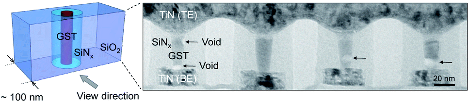 | ||
| Fig. 1 Ex situ TEM observation of a PCM device failed after endurance test. Confined GST nanopillars with a diameter of 20 nm are surrounded by SiNx spacer. As shown in the schematic drawing, the entire structure, i.e. the GST nanopillars and surrounding SiOx layers, is contained within the TEM sample (thickness ∼ 100 nm) without cutting and surface exposure. The TEM image taken after the cycling test shows that the voids (black arrows) are preferentially formed at the interface with the TiN BE. | ||
SEM nano-probing of TEM specimens for in situ TEM biasing experiments
Fig. 2a shows a SEM image of typical TEM specimen prepared for in situ TEM tests. Prior to in situ TEM experiments, all TEM samples prepared by FIB were tested using a built-in nanoprobe system in SEM to determine whether the PCM device works in normal operation. We selected TEM samples showing a clear DC threshold switching at around 1.4 V without volatilization of GST. The TEM samples were then switched to the reset state just before in situ TEM tests.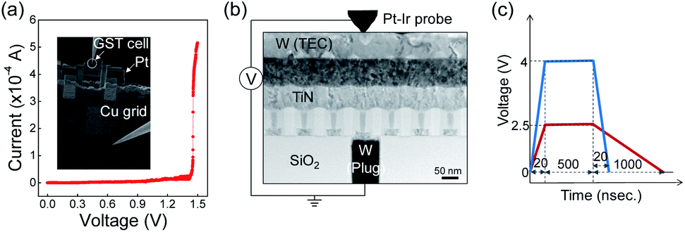 | ||
| Fig. 2 TEM specimen and voltage pulses used for in situ TEM biasing experiments. (a) A typical I–V curve for the TEM sample of a confined GST cell prepared for in situ TEM switching experiments. As shown by the inset, the I–V curve was measured using a nano-probing system installed in the SEM. (b) Cross-sectional TEM sample of confined GST cells prepared for in situ switching in TEM. The W plug connected to the TiN BE is held at the ground by attaching it to a Cu support grid. A Pt–Ir tip makes electrical contact with the W top electrode contact (TEC), forming an electrical circuit for the application of voltage pulses. (c) A schematic illustration of voltage pulses applied for set and reset switching in TEM. Note that the falling edges (time) of set (red) and reset (blue) pulses are fixed to 1000 ns and 20 ns, respectively. | ||
Given that the GST nanopillar was initially switched to the reset state, the current flowing through the entire circuit would be limited by the amorphous state of the switching volume. However, the as-fabricated TEM devices usually exhibited a low resistance close to the set state due to the formation of the crystalline phase during FIB processing. Therefore, before in situ TEM switching experiments the GST PCM cells were switched back to the reset state using the SEM nano-probing system. Then, the PCM cells in the reset sate were electrically stressed with the passage of multiple set pulses in TEM.
A schematic was added to the TEM image in Fig. 2b to illustrate how the voltage pulses are applied to the active GST nanopillar through a Pt–Ir probe installed in the in situ TEM holder. A TEM sample contains a series of cylindrically confined GST nanopillars in which only the one that connected to the W plug is electrically switchable. While the voltage pulses are applied to the top TiN/W electrode of GST, the bottom TiN/W electrode is held at ground. Fig. 2c shows the two voltage pulses used in this study; one with +4 V amplitude, 500 ns duration time and 20 ns falling edge represents the reset pulse (blue in Fig. 2c), and the other with +2.5 V amplitude, 500 ns duration time and 1000 ns falling edge represents the set pulse (red in Fig. 2c). To capture the void evolution process in detail, we slowed down the programming process by using the set pulse with a slightly lower amplitude (+2.5 V) than that of a typical set pulse (+3.5 V).
Direct observation of void formation and migration during passage of multiple set pulses
The snapshot TEM images obtained after each set pulse are shown in Fig. 3 (see ESI Movie S1†). After the first set pulse was applied, a void was formed at the GST/SiNx interface (sidewall) near the BE (Fig. 3a). Initially, small nanoscale voids contained within the GST cell coalesced to form a large void upon application of a set voltage pulse (see ESI Movie S2†). Once a large void forms, it continues growing during subsequent set pulses and remains at the position where it initially appeared (Fig. 3a). The volume change of GST induced by the void formation and growth from the 1st to the 4th set pulses is measured to be ∼5–9%, which is quite comparable to the well-known volume shrinkage upon the crystallization of amorphous GST (∼6.8% volume difference between amorphous and face-centered cubic GST). This suggests that the initial void formation and growth is likely induced by densification of amorphous GST to its crystalline state.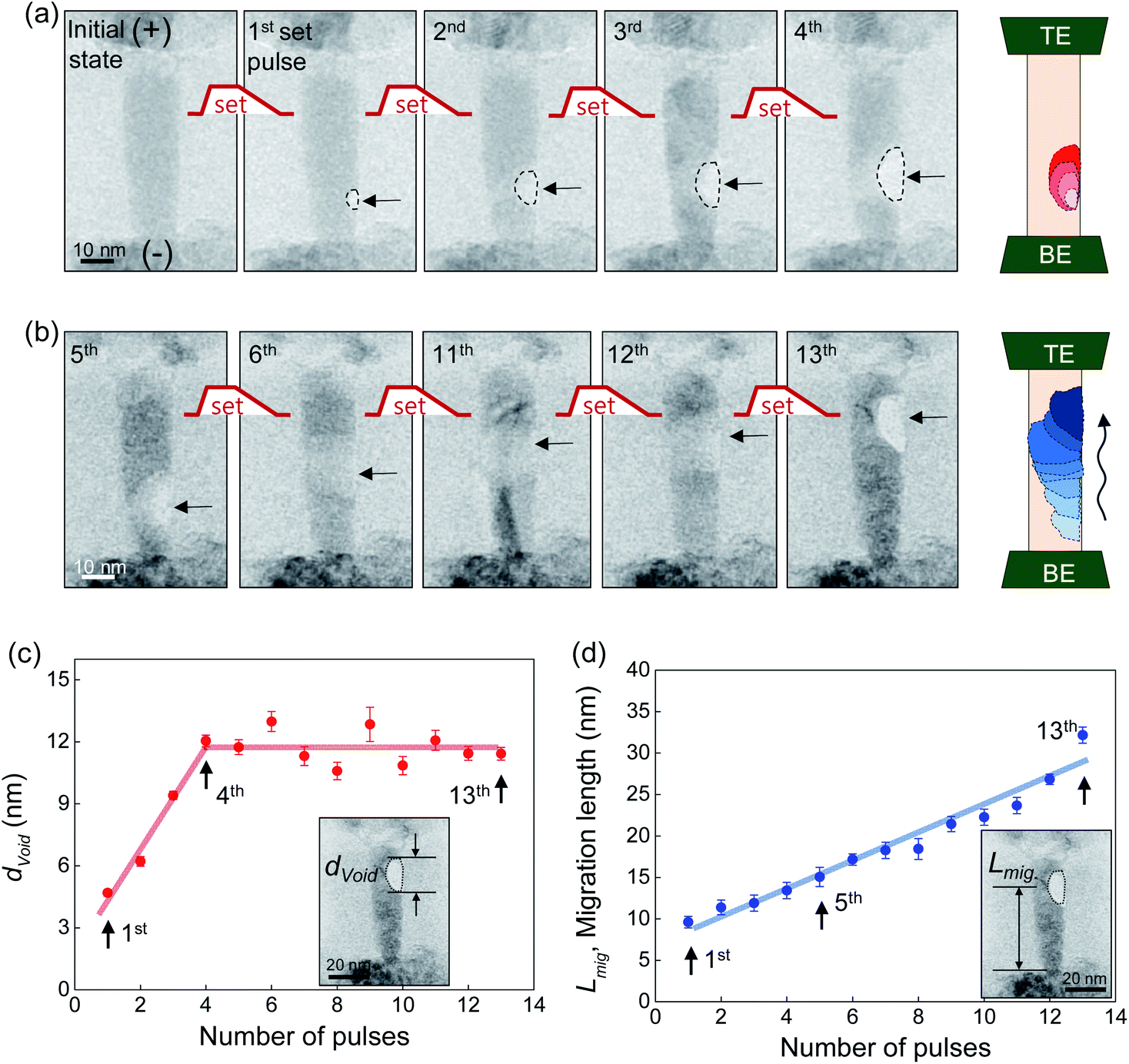 | ||
| Fig. 3 Direct observation of void formation and migration during the passage of multiple set pulses. A total of 13 set pulses were applied sequentially. (a) A series of TEM images captured after the application of the 1st, 2nd, 3rd, and 4th pulses. After the 1st pulse was applied, the void (indicated by black arrows) nucleated at the GST/SiNx interface near the BE and then grew in response to the subsequent pulses. The growth of the void is traced and schematically represented by red color gradients in the right-most panel. (b) A series of TEM images captured after the application of the 5th, 6th, 11th, 12th and 13th set pulses. The void (indicated by black arrows) migrates toward the TE with the application of the set pulses. The migration of the void is traced and schematically illustrated with blue color gradients in the right-most panel. (c) Plot of the size (dvoid) as a function of the number of applied set pulses. The size of the void increases gradually up to the 4th pulse and then remains constant during the subsequent pulses. (d) Plot of the migration length (Lmig) of void from the bottom to the TE. Note that the increase in migration length from the 1st to the 13th pulse is nearly linear. Red and blue solid lines are added as guides to the eyes. | ||
The preferential nucleation of void near the BE can be explained by non-uniform temperature distribution within the confined GST cell; due to the tapered cylindrical shape of the GST cell the local temperature is relatively higher near the narrower cylinder region because of the higher current density. To calculate the temperature distribution within the GST cell, we used the following equation based on finite element modeling (FEM):
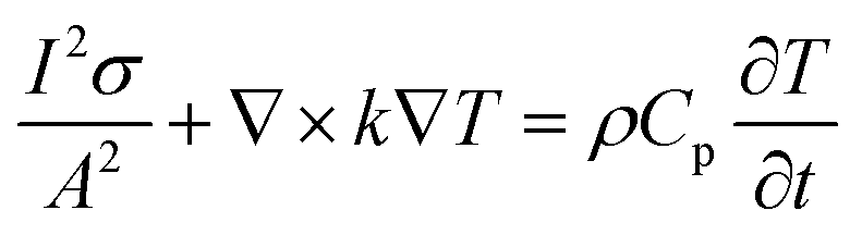 | (1) |
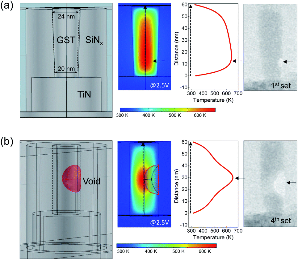 | ||
| Fig. 4 FEM of temperature distribution within a confined GST cell. (a) Temperature map and profile calculated for the GST cell with a tapered nanopillar shape under the application of a set pulse. The temperature profile across the GST cell as shown along the vertical black dotted arrow indicates that the maximum temperature (hot spot) appears near the lower part of the GST cell, which coincides with the preferential site for void formation. (b) Temperature map and profile calculated for the GST cell containing a void. Note that the hot spot along the vertical direction is now located near the void. | ||
The void grows in size with further application of pulses (up to the 4th pulse in Fig. 3a). Although the void appeared to reside at the same location during growth, tracing the void boundary indicates that its center-of-mass is shifted slightly upward toward the positively biased TE. The growth of the void is accompanied by the change in the TEM contrast of the surrounding GST; the region exhibiting bright TEM contrast appears and extends with the growth of void. If it is assumed that the TEM contrast is dominated by mass-thickness, the change of contrast indicates a redistribution of the constituent elements surrounding the void.
Once the void reaches a certain size, it stops growing but continues migrating toward the TE. During the void migration, the GST exhibits a noticeable change in the diffraction contrast induced by constant crystallization and crystal reorientation (refer to Fig. 3b and ESI Movie S3†). The size and migration distance of the void were measured and plotted as a function of the applied pulse number (Fig. 3c and d). Quantitative measurements using TEM intensity profiling revealed that the size of the void increased gradually to ∼12 nm until the 4th pulse, and thereafter it ceased growing and remained constant in size. The position of the void in the cylinder changed as it migrated continuously toward the TE, moving a distance of over 15 nm during the pulsing experiments. In summary, the coarsening and migration of voids were simultaneously accompanied by: (1) the change in TEM contrast near the void, originating from the redistribution of the constituent elements; (2) extension of the crystallized volume of GST to the entire switching volume (refer to Fig. 3b), respectively.
The effects of void on the temperature distribution within a GST cell were calculated for its size ranges measured experimentally (Fig. S1†). The results show that the Joule heating becomes strongly confined to the narrow channel next to the void as the size of the void increases, resulting in a higher peak temperature in the constrained channel near the void (Fig. 4b). The results also indicate that the peak temperature can increase to a point far beyond the glass transition temperature of GST (Tg ∼ 428 K),31 indicating that the local Joule heating can accelerate thermally activated electromigration of ions. Furthermore, the current density also increases dramatically as the size of void increases. For example, the current density increases up to ∼14.5 MA cm−2 from the ∼9 MA cm−2 which corresponds to the reference value in the absence of void. The measured current density is much higher than the typical value for a line pattern structure of crystalline GST (∼1.8 MA cm−2) and high enough to drive the electric field-induced migration of the constituent elements of GST.32
Direct observation of reset-stuck failure by void formation
To investigate the response of voids during the switching between reset and set states, cycles of reset and set pulses were applied repeatedly to the device (Fig. 5). For this experiment, we used a reset-stuck GST cell containing large matured voids which had been formed in previous in situ TEM endurance tests. The PCM device used for Fig. 5 was initially in amorphous state. The absence of TEM diffraction contrast during the cyclic switching (up to the 2nd reset pulse as shown in Fig. 5d) indicates that the GST cell is stuck in the reset state and remained in the amorphous state. After the 4th pulse (the 2nd set pulse in Fig. 5e), the GST cell exhibited strong diffraction contrast indicating the crystalline state of GST. The crystalline state was further confirmed by the Moiré fringes in the HRTEM image. The resistance of reset-stuck failed GST cells due to the void formation remained in roughly the same order of magnitude as in the reset state (∼107 ohm) without being restored to the set state (∼104 ohm) by application of a set pulse.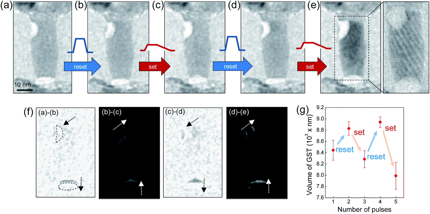 | ||
| Fig. 5 Reset-stuck failure caused by void formation. (a)–(e) A series of TEM images captured after the set and the reset pulses were applied to a failed PCM device. Different responses of voids to the set and reset pulses is noticeable, i.e. expansion and contraction, respectively. A high-resolution TEM image showing the Moiré fringes is added in (e). The relatively dark diffraction contrast near the edge of the (upper) void is likely due to the enrichment of the heaviest element Te in GST. (f) TEM difference images obtained by mathematical subtraction of two TEM images such as: (a)–(b), (b)–(c), (c)–(d) and (d)–(e). The voids do not disappear but only show slight volume changes in response to the reset and set pulses. Note that the dark contrast and the bright contrast formed near the voids indicate a decrease and increase of GST volume, respectively (indicated by black and white dotted arrows, respectively). The arrows indicate the direction of volume change. (g) Measured GST volume versus the number of applied pulses. Note that the volume changes of GST during set and reset switching are clearly observed; i.e., the set pulse causes expansion of the void and the reset pulse causes contraction. | ||
The two large voids in Fig. 5, one close to the BE and the other one close to the TE, showed contraction and expansion in response to the reset and the set pulses, respectively (Fig. 5a–e and ESI Movie S4 and S5†). The TEM difference images obtained by frame subtraction before and after the application of each pulse clearly visualizes the volume change of the voids (Fig. 5f). We found that the direction of volume expansion points to the TE (white arrows in Fig. 5f). This behavior was reproducible in repeated cyclic switching. The absence of TEM diffraction contrast during the cyclic switching indicates that the GST cell is stuck in the reset state and remained in an amorphous state. The variation of GST cell volume induced by the dynamic evolution of voids is seen to be continuously diverging within a range of 4.5–11.9% (Fig. 5g), indicating that the elemental redistribution induced by set and reset pulses occurs quite differently and leads to the volume changes.
The void formation in GST can be caused by the electromigration of cations and anions,22 coalescence of Te vacancies,23,24 and the material stress resulting from volume changes12,25 during the transition between the amorphous and crystalline phases. In molten or amorphous GST, the Ge+, Sb+ and Te− ions can migrate toward the appropriate electrode under the influence of electrostatic force, resulting in redistribution of the elements.32 The electromigration can further induce local segregation, phase separation and void formation. For example, as Xie et al. recently reported, the electromigration of the constituent elements can lead to the formation of voids in confined GST nanopillars.9 According to their in situ observation, when a positive voltage pulse is applied to the BE, electromigration leads to the depletion of Sb+ and the enrichment Te− near the BE. They claimed that a void can form because the electromigration of Sb+ toward the TE occurs more readily than that of Te−. This is plausible since Sb+ has a higher DZ* value (+1.98 × 10⁻⁵ cm2 s−1; D is the atomic diffusion coefficient and Z* is the effective charge number) than Te− does (−1.17 × 10⁻⁵ cm2 s−1).21,29 The healing of voids resulting from reversing the voltage polarity further supports the notion that the void formation was induced by electromigration, particularly the more facile migration of Sb. We note that the GST nanopillars in ref. 9 have a shape similar to those in the present study, i.e., a tapered cylindrical shape with a narrower width near the BE. In the present experiments, in contrast to the work in ref. 9, positive voltage pulses were applied to the TE. Nonetheless, the fact that the void was formed preferentially near the BE in the two experiments indicates that the local Joule heating (current density) plays a decisive role in determining the preferential nucleation site for voids, as shown in Fig. 4a.
The migration of voids toward the positively biased TE strongly supports the contention that the coalescence of Te vacancies resulting from electromigration constitutes the most probable mechanism for void formation and growth. Previous work showed that large voids and small cavities surrounded by Te atoms with two and three coordination numbers are observed in both molten and amorphous GST with low density.24 The under-coordinated Te atoms have considerable vacant space around them. According to molecular dynamics simulation, a large void will form in amorphous or molten GST when Te atoms agglomerate.24 It is known that a significant amount of vacancies (20%) also exists around the Te atoms in the crystalline GST as well, and this configuration of Te atoms is similar to those in amorphous GST. As these under-coordinated Te atoms agglomerate, a large void will form and grow (Fig. 6a). The observed direction of void migration pointing to the positively biased TE, which coincides with the direction of electromigration by negatively-charged Te atoms, indicates that the growth and migration is assisted by agglomeration of Te atoms under the influence of electromigration (Fig. 6b). Furthermore, the direction of expansion or deformation of voids, which also points toward the TE, further implicates the agglomeration of negatively-charged Te atoms results in the expansion of voids. We note the dark contrast outlining the void/GST interface in the high-resolution TEM image in Fig. 5e, which indicates the potential enrichment of the heaviest element Te of GST. However, more explicit verification on the role of elemental Te distribution in the growth and migration of voids requires in situ elemental mapping during the switching of a GST-based PCM device.
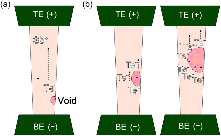 | ||
| Fig. 6 A proposed model for void formation and migration based on in situ TEM observations. (a) Formation of a void at the hot spot. Electromigration of Sb+ and Te− in GST results in elemental redistribution. (b) Growth and migration of a void by agglomeration of Te− near the void. The observed migration of the void toward the positively biased electrode, which matches the direction of the electromigration of negatively-charged Te− atoms, indicates that void growth and migration are assisted by the agglomeration of Te− atoms facilitated by electromigration. It is noted that the undercoordinated Te− atoms have ample vacancies around them. | ||
The different response of the voids during cyclic reset-set switching, i.e. contraction in the reset pulses and expansion in the set pulses, could be related to the different migration kinetics of under-coordinated Te atoms. When the reset pulse is applied, the peak temperature near the void is much higher but decreases much faster with time than it does by the set pulse. There might not be enough time for Te atoms to diffuse and incorporate into the crystalline lattice of GST to generate the vacancies required for the void growth. However, during the set pulse the temperature decays slowly so that the Te atoms can diffuse into the lattice and become incorporated so as to generate vacancies, leading to the volume expansion of void. Although the positive voltage pulses are applied to the TE in the present experiments so that the voids grow with the pulses, the void would be healed as a a consequence of reverse atomic migration if the opposite polarity of voltage pulse is applied.9
4. Conclusion
The present in situ TEM observations showed that a void nucleates preferentially at the hot spot of the confined cell, indicating that the local current density (Joule heating) plays a decisive role in the formation process. Once a void forms, subsequent set pulses favor its growth over the nucleation of new voids and the fully grown void continues migrating toward the positively biased electrode. The observed polarity-dependent migration of the void can be explained by the field-induced redistribution of the constituent elements during the crystallization of GST, especially by the electromigration of under-coordinated Te− ions which have vacancies around them. When the reset pulse with the same voltage polarity is applied, the voids exhibit a slight volume shrinkage but are not completely healed, resulting in a reset-stuck failure. The variation of GST cell volume induced by dynamic evolution of voids is measured to be continuously diverging in the range of 4.5–11.9%, indicating that the elemental redistribution under set and reset pulses occurs in quite different manners, i.e. the different migration kinetics of Te atoms. The present results demonstrate that the elemental redistribution induced by electromigration during the phase transition must be controlled carefully to suppress void formation and migration, especially Te, since it is a major element (2.5× larger than Ge and Sb in the atomic concentration) exhibiting low coordination numbers and a negative charge.Conflicts of interest
There are no conflicts to declare.Acknowledgements
This work has been supported by SK hynix Semiconductor Inc. and by the Creative Materials Discovery Program through the National Research Foundation (NRF) of Korea funded by the Ministry of Science, ICT and Future Planning (NRF-2015M3D1A1070672, NRF-2019M3D1A1078296), Bio-inspired Innovation Technology Development Project (NRF-2018M3C1B7021994), NRF grant (NRF-2015R1A2A2A01007 904) and Industrial Technology Innovation Program (10080654) of the Ministry of Trade, Industry & Energy (MOTIE, Korea).Notes and references
- M. Wuttig and N. Yamada, Nat. Mater., 2007, 6, 824–832 CrossRef CAS.
- D. Loke, T. H. Lee, W. J. Wang, L. P. Shi, R. Zhao, Y. C. Yeo, T. C. Chong and S. R. Elliott, Science, 2012, 336, 1566–1569 CrossRef CAS PubMed.
- S. H. Lee, Y. Jung and R. Agarwal, Nat. Nanotechnol., 2007, 2, 626–630 CrossRef CAS PubMed.
- H. F. Hamann, M. O'Boyle, Y. C. Martin, M. Rooks and K. Wickramasinghe, Nat. Mater., 2006, 5, 383–387 CrossRef CAS.
- D. K. Loke, J. M. Skelton, T. H. Lee, R. Zhao, T.-C. Chong and S. R. Elliott, ACS Appl. Mater. Interfaces, 2018, 10, 41855–41860 CrossRef CAS.
- T. Tuma, A. Pantazi, M. Le Gallo, A. Sebastian and E. Eleftheriou, Nat. Nanotechnol., 2016, 11, 693–699 CrossRef CAS PubMed.
- W. Zhang, R. Mazzarello, M. Wuttig and E. Ma, Nat. Rev. Mater., 2019, 4, 150–168 CrossRef CAS.
- S. Kohara, K. Kato, S. Kimura, H. Tanaka, T. Usuki, K. Suzuya, H. Tanaka, Y. Moritomo, T. Matsunaga, N. Yamada, Y. Tanaka, H. Suematsu and M. Takata, Appl. Phys. Lett., 2006, 89, 201910 CrossRef.
- Y. Xie, W. Kim, Y. Kim, S. Kim, J. Gonsalves, M. BrightSky, C. Lam, Y. Zhu and J. J. Cha, Adv. Mater., 2018, 30, 1705587 CrossRef PubMed.
- S. J. Park, M. Ahn, K. Jeong, M. H. Jang, M.-H. Cho, J. Y. Song, D.-H. Ko, D.-h. Ahn, S.-W. Nam and G. Jeong, J. Mater. Chem. C, 2014, 2, 2001–2009 RSC.
- T. Y. Yang, J. Y. Cho, Y. J. Park and Y. C. Joo, Acta Mater., 2012, 60, 2021–2030 CrossRef CAS.
- K. Do, D. Lee, D.-H. Ko, H. Sohn and M.-H. Cho, Electrochem. Solid-State Lett., 2010, 13, H284–H286 CrossRef CAS.
- S.-H. Hong and H. Lee, Jpn. J. Appl. Phys., 2008, 47, 3372–3375 CrossRef CAS.
- K. Kinarn and A. Su Jin, Proc. IEEE, 2005, 17–21, 157–162 Search PubMed.
- J.-B. Park, G.-S. Park, H.-S. Baik, J.-H. Lee, H. Jeong and K. Kim, J. Electrochem. Soc., 2007, 154, H139–H141 CrossRef CAS.
- B. Rajendran, M. Lee, M. Breitwisch, G. W. Burr, Y. Shih, R. Cheek, A. Schrott, C. Chen, M. Lamorey, E. Joseph, Y. Zhu, R. Dasaka, P. L. Flaitz, F. H. Baumann, H. Lung and C. Lam, Proc. IEEE VLSI Technology, 2008, 17–19, pp. 96–97 Search PubMed.
- S. Kim, G. W. Burr, W. Kim and S.-W. Nam, MRS Bull., 2019, 44, 710–714 CrossRef.
- J. Sarkar and B. Gleixner, Appl. Phys. Lett., 2007, 91, 233506 CrossRef.
- C. W. Jeong, Proc. NVSMW, 2004, p. 28 Search PubMed.
- S. Kim, N. Sosa, M. BrightSky, D. Mori, W. Kim, Y. Zhu, K. Suu and C. Lam, Proc. IEEE IEDM, 2013, 9–11, pp. 30.7.1–30.7.4 Search PubMed.
- T. Y. Yang, I. M. Park, B. J. Kim and Y. C. Joo, Appl. Phys. Lett., 2009, 95, 032104 CrossRef.
- D. Kang, D. Lee, H.-M. Kim, S.-W. Nam, M.-H. Kwon and K.-B. Kim, Appl. Phys. Lett., 2009, 95, 011904 CrossRef.
- L. Krusin-Elbaum, C. Cabral Jr, K. N. Chen, M. Copel, D. W. Abraham, K. B. Reuter, S. M. Rossnagel, J. Bruley and V. R. Deline, Appl. Phys. Lett., 2007, 90, 141902 CrossRef.
- Z. Sun, J. Zhou, A. Blomqvist, B. Johansson and R. Ahuja, Phys. Rev. Lett., 2009, 102, 075504 CrossRef PubMed.
- M. Rizzi, A. Spessot, P. Fantini and D. Ielmini, Appl. Phys. Lett., 2011, 99, 223513 CrossRef.
- C. Chen, A. Schrott, M. H. Lee, S. Raoux, Y. H. Shih, M. Breitwisch, F. H. Baumann, E. K. Lai, T. M. Shaw, P. Flaitz, R. Cheek, E. A. Joseph, S. H. Chen, B. Rajendran, H. L. Lung and C. Lam, Proc. IEEE, 2009, 10–14, 1–2 Search PubMed.
- M. B. Sky, N. Sosa, T. Masuda, W. Kim, S. Kim, A. Ray, R. Bruce, J. Gonsalves, Y. Zhu, K. Suu and C. Lam, Proc. IEEE IEDM, 2015, 7–9, pp. 3.6.1–3.6.4 Search PubMed.
- W. Kim, S. Kim, R. Bruce, F. Carta, G. Fraczak, A. Ray, C. Lam, M. BrightSky, Y. Zhu, T. Masuda, K. Suu, Y. Xie, Y. Kim and J. J. Cha, Proc. IEEE IRPS, 2018, 11–15, pp. 6D.5-1-6D.5–5 Search PubMed.
- K. Baek, K. Song, S. K. Son, J. W. Oh, S.-J. Jeon, W. Kim, H. J. Kim and S. H. Oh, NPG Asia Mater., 2015, 7, e194 CrossRef CAS.
- S. Son, S. Jeon, J. Oh, W. Kim, H. Kim, J. Lee, S. Woo, G. Do, S. Lee, K. Baek and S. H. Oh, Proc. ISTFA, 2013, pp. 236–238 Search PubMed.
- J. Kalb, F. Spaepen, T. P. L. Pedersen and M. Wuttig, J. Appl. Phys., 2003, 94, 4908–4912 CrossRef CAS.
- Y.-J. Park, T.-Y. Yang, J.-Y. Cho, S.-Y. Lee and Y.-C. Joo, Appl. Phys. Lett., 2013, 103, 073503 CrossRef.
Footnotes |
| † Electronic supplementary information (ESI) available. See DOI: 10.1039/d0na00223b |
| ‡ These authors contributed equally. |
| This journal is © The Royal Society of Chemistry 2020 |