
 Open Access Article
 This Open Access Article is licensed under a Creative Commons Attribution-Non Commercial 3.0 Unported Licence
Synthesis of silicon carbide nanocrystals and multilayer graphitic carbon by femtosecond laser irradiation of polydimethylsiloxane
Shuichiro
Hayashi
 a,
Fumiya
Morosawa
b and
Mitsuhiro
Terakawa
*ab
a,
Fumiya
Morosawa
b and
Mitsuhiro
Terakawa
*ab
aSchool of Integrated Design Engineering, Keio University, 3-14-1, Hiyoshi, Kohoku-ku, Yokohama-shi, 223-8522, Japan. E-mail: terakawa@elec.keio.ac.jp
bDepartment of Electronics and Electrical Engineering, Keio University, 3-14-1, Hiyoshi, Kohoku-ku, Yokohama-shi, 223-8522, Japan
First published on 19th March 2020
Abstract
Laser-based modification of polymer materials has been emerging as a versatile and efficient technique to simultaneously form and pattern electrically conductive materials. Recently, it has been revealed that native polydimethylsiloxane (PDMS) can be modified into electrically conductive structures using femtosecond laser irradiation; however, the details regarding the structures formed by this method have yet to be revealed. In this work, structures were fabricated by focusing and scanning femtosecond laser pulses onto the surface of PDMS. Raman Spectroscopy and Transmission Electron Microscopy (TEM) analyses revealed the formation of silicon carbide (SiC) nanocrystals, as well as multilayer graphitic carbon, in the modified regions of PDMS. The state of the formed material differed depending on the distance from the focal spot, suggesting that photo-thermal effects contributed to the degradation of PDMS into conductive material. Electrical conductivity measurements, in addition to Raman results, indicated that the amount of disorder in the formed graphitic carbon contributes to the electrical conductivity of the fabricated structures.
1. Introduction
Laser irradiation offers a one-step method to permanently modify and functionalize polymer materials. The irradiation of the laser beam induces localized photo-thermal and/or photo-chemical effects near the focal spot, degrading the polymer material and causing permanent changes in its properties, such as its refractive index and electrical conductivity.1,2 The modification of polymers into electrically conductive materials is particularly promising since it will allow for the simultaneous formation and patterning of electrically conductive structures on flexible polymer substrates for novel electronic device applications, such as flexible devices.3,4 While conventional furnace-system methods can also allow for the conversion of polymer materials into electrically conductive materials,5 the laser-based method allows for spatially selective and high-resolution modification of the polymer material without significantly affecting the bulk substrate.Various studies have been reported regarding the modification and functionalization of polymer materials by laser irradiation. For example, Schumann et al. reported the permanent modification of polyimide (PI), an industrial polymer, into electrically conductive structures using a 248 nm KrF excimer laser.6 Similarly, Lin et al. reported the modification of PI into electrically conductive structures using a ∼10.6 μm CO2 laser, and further analyses of the fabricated structures showed that the PI degraded into porous graphitic carbon layers by laser irradiation.7 The degradation mechanism of polymers is complex, and it is difficult to conclude whether the degradation of PI into graphitic carbon is due to a photothermal and/or photochemical process. However, since photochemical processes tend to occur for shorter wavelengths and ultra-short pulses, the modification process in Schumann's report is most likely a photochemical process and that in Lin's report is most likely a photothermal process. Polymer materials that can be utilized as the carbon precursor, for the formation of graphitic carbon, are not limited to PI, and the formation of graphitic carbon by laser irradiation has also been reported for polyfluorene (PF),8 polydimethylsiloxane (PDMS),9 and cellulose nanofibers (CNFs),10 to name a few.
The product formed by modification of polymers is also not limited to graphitic carbon. There have been reports regarding the fabrication of advanced ceramic materials, such as titanium carbonitride (Ti(C,N)),11 silicon carbonitride (Si(C,N)),12,13 and silicon carbide (SiC),14,15 from organometallic polymers. For example, Jakubenas et al. reported the modification of polycarbosilane (PCS), an organosilane polymer, into crystalline 3C-SiC (β-SiC) using a ∼10.6 μm continuous wave (CW) CO2 laser.16 Recently, Nakajima et al. reported the direct modification of native PDMS, which is also an organosilane polymer, into electrically conductive structures composed of β-SiC using a 522 nm femtosecond laser.17 PDMS is a well-known and widely utilized elastomer for various applications, owing to its biocompatibility, optical transparency, and elasticity. The femtosecond-laser-based modification of PDMS into electrically conductive structures allows for the direct and precise functionalization of PDMS; however, to the best of our knowledge, the detailed investigations of the modified PDMS regions, particularly micron and submicron analyses of the modified regions, and the effect of the formed materials on the structures' electrical properties, have yet to be revealed.
In this work, the formation of SiC nanocrystals and multilayer graphitic carbon by irradiating femtosecond laser pulses on PDMS was revealed. Line structures were fabricated by focusing and scanning laser pulses on the surface of PDMS, and the effects of the fabrication parameters on the dimensions of the modified regions were investigated. Analyses were performed on the fabricated line structures by Raman Spectroscopy and Transmission Electron Microscopy (TEM) to determine the material formed due to laser irradiation. Various locations of the surface, as well as the cross section, of the modified region were analysed to assess the uniformity of the formed material. Two-dimensional structures were fabricated with various numbers of raster scans, with a constant line-to-line distance, and electrical conductivity measurements, in addition to Raman spectroscopy, of the structures were performed to discuss the effect of the formed material on the electrical conductance of the fabricated structures.
2. Experimental
2.1. Modification of PDMS using femtosecond laser pulses
Liquid photo-curable PDMS (KER-4690 A/B, 1![[thin space (1/6-em)]](https://www.rsc.org/images/entities/char_2009.gif) :1 ratio, Shin-Etsu Chemical Co., Ltd., Japan) was mixed, and the uncured solution was poured into a rectangular mold. The uncured PDMS was de-gassed in a vacuum chamber and then placed under a 365 nm ultraviolet lamp for 30 min under ambient conditions to induce crosslinking. The cured PDMS sheets had an average thickness of approximately 1.9 mm. The as-prepared PDMS sheets were cut into smaller sheets, and after the surfaces were washed using ethanol (99.5%) they were placed on a cover glass with a 140 μm-air-spacing, as shown in Fig. 1. Laser pulses with a central wavelength of 522 nm, the second harmonic wave of a 1045 nm femtosecond laser (High Q-2, Spectra-Physics, USA), a 192 fs pulse length, and a 63 MHz repetition rate were used for the fabrication of all the structures introduced in this work. Femtosecond laser pulses were focused on the bottom surface of the PDMS under ambient conditions using a 20× objective lens with a numerical aperture (NA) of 0.4 (Olympus, Japan). The laser focal diameter is assumed to be ∼1.6 μm, according to the formula d = 1.22λ/NA. A 3-axis (xyz) translation stage was utilized to scan the PDMS in the xy-plane. The fabrication process was monitored in real time using a CMOS camera (Thorlabs, USA).
:1 ratio, Shin-Etsu Chemical Co., Ltd., Japan) was mixed, and the uncured solution was poured into a rectangular mold. The uncured PDMS was de-gassed in a vacuum chamber and then placed under a 365 nm ultraviolet lamp for 30 min under ambient conditions to induce crosslinking. The cured PDMS sheets had an average thickness of approximately 1.9 mm. The as-prepared PDMS sheets were cut into smaller sheets, and after the surfaces were washed using ethanol (99.5%) they were placed on a cover glass with a 140 μm-air-spacing, as shown in Fig. 1. Laser pulses with a central wavelength of 522 nm, the second harmonic wave of a 1045 nm femtosecond laser (High Q-2, Spectra-Physics, USA), a 192 fs pulse length, and a 63 MHz repetition rate were used for the fabrication of all the structures introduced in this work. Femtosecond laser pulses were focused on the bottom surface of the PDMS under ambient conditions using a 20× objective lens with a numerical aperture (NA) of 0.4 (Olympus, Japan). The laser focal diameter is assumed to be ∼1.6 μm, according to the formula d = 1.22λ/NA. A 3-axis (xyz) translation stage was utilized to scan the PDMS in the xy-plane. The fabrication process was monitored in real time using a CMOS camera (Thorlabs, USA).
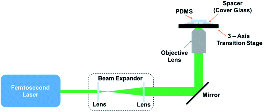 | ||
| Fig. 1 Schematic illustration of the laser irradiation setup. | ||
2.2. Materials characterization
The dimensions and surface morphology of the fabricated structures were observed and characterized by digital microscopy (MS-100, Asahikogaku, Japan) and scanning electron microscopy (SEM, Inspect F50, FEI, USA). The fabricated structures were cut perpendicular to the laser scanning direction to observe the cross sections of the modified regions. Chemical analyses of the fabricated structures were performed using a laser-excited Raman spectrometer (InVia Raman Microscope, Renishaw, UK) using a 50× objective lens with a NA of 0.75. An excitation wavelength of 532 nm and wavenumber range of 700–2800 cm−1 were used for the analyses. Using the above-mentioned Raman settings, the predicted spatial resolution is estimated to be in the order of 1 μm. Nanoscale observations and analysis of the fabricated structures were conducted by TEM (Tecnai G2, FEI, USA). TEM samples were prepared using the focused ion beam technique (FIB). For electrical conductivity measurements, gold electrodes, with an approximate thickness of 50 nm, were fabricated on both ends of the fabricated structures. The electrical resistances of the fabricated structures were measured by the two-probe method using a digital source meter (175 True RMS Digital Multimeter, Fluke, USA).3. Results and discussion
3.1. Parameter dependency of modification dimensions
4 mm-long line structures were fabricated by focusing and scanning femtosecond laser pulses on the surface of PDMS. Fig. 2 shows digital microscope images of line structures fabricated with laser powers of 50 mW (surface: Fig. 2(a), cross section: Fig. 2(d)), 100 mW (surface: Fig. 2(b), cross section: Fig. 2(e)), and 150 mW (surface: Fig. 2(c), cross section: Fig. 2(f)). The scanning speed was set at 2 mm s−1 for the fabrication of the structures shown in Fig. 2. For laser powers of 50 mW and above, the PDMS was modified into black structures by femtosecond-laser-irradiation; however, for laser powers less than 50 mW, no modification of PDMS was visibly observed (data not shown). A unidirectional groove can be observed at the center of each fabricated line structure, which is attributable to the ablation of the formed material due to the high peak intensity. As shown in Fig. 2(g), with the increase in laser power, the width (shown in black), as well as the depth (shown in red), of the fabricated structure increased linearly.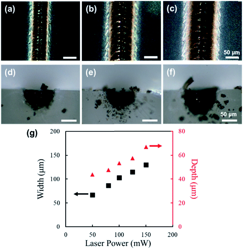 | ||
| Fig. 2 Digital microscope images of the fabricated line structures. Surface of the structures fabricated with laser power of (a) 50 mW, (b) 100 mW, and (c) 150 mW, respectively. Cross sections of the structures fabricated with laser power of (d) 50 mW, (e) 100 mW, and (f) 150 mW, respectively. Structures were fabricated with a scan speed of 2 mm s−1. (g) Change in line width (black) and depth (red) with respect to laser power. | ||
Fig. 3 shows digital microscope images of line structures fabricated with a scanning speed of 1 mm s−1 (surface: Fig. 3(a), cross section: Fig. 3(d)), 4 mm s−1 (surface: Fig. 3(b), cross section: Fig. 3(e)), and 8 mm s−1 (surface: Fig. 3(c), cross section: Fig. 3(f)). The laser power was set to 150 mW for the fabrication of the structures shown in Fig. 3. Similar to that in the structures shown in Fig. 2, a unidirectional groove can also be observed at the center of each line structure in Fig. 3. As shown in Fig. 3(g), with the increase in scanning speed, the width decreased linearly (shown in black); however, the width did not change significantly (shown in red).
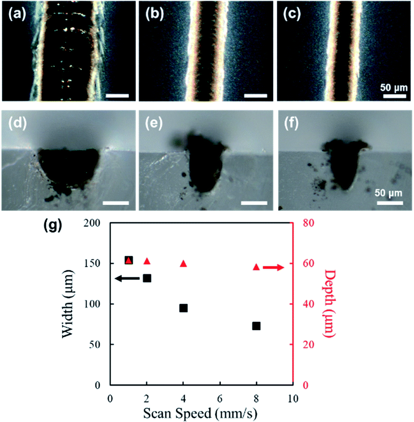 | ||
| Fig. 3 Digital microscope images of the fabricated line structures. Surface of the structures fabricated with scan speed of (a) 1 mm s−1, (b) 4 mm s−1, and (c) 8 mm s−1, respectively. Cross sections of the structures fabricated with scan speed of (d) 1 mm s−1, (e) 4 mm s−1, and (f) 8 mm s−1, respectively. Structures were fabricated with a laser power of 150 mW. (g) Change in line width (black) and depth (red) with respect to scan speed. | ||
From the results of Fig. 2 and 3, it can be deduced that the maximum depth of modification is determined mainly by the laser power, and the width is determined by both the laser power and scanning speed used for the fabrication process. After the initial modification of PDMS occurs due to nonlinear absorption, in which the rudimentary dimensions of the formed structure depend mainly on the peak laser intensity, the succeeding laser pulses will be absorbed by the modified region closer to the surface, linearly and nonlinearly. The absorption of subsequent pulses will result in heat accumulation and consequently the expansion of the modified region. The amount of thermal accumulation depends on the energy per pulse and the amount of pulse overlap, which are related to the laser power and scanning speed, respectively; therefore, with an increase in laser power and decrease in scanning speed, an increase in the dimensions of the modified region should occur. However, since the laser energy will be absorbed significantly more by the modified region closer to the surface, heat effects, and ergo expansion of the modified region, will be more considerable for the regions closer to the surface, resulting in different shapes of the modified region as observed for Fig. 3(d) and (f). For all the fabrication parameters, the dimensions of the fabricated structures were significantly larger than the spot size at the focal point, which is attributable to the thermal effects resulting from the high repetition rate (63 MHz). By adjusting the repetition rate, so that sufficient, but not excessive, thermal effects for modification will be induced, while controlling the laser intensity and scanning speed, improvement in the fabrication resolution, down to a few microns, could be realized.
3.2. Examination of surface morphology
Fig. 4 shows the SEM images of the surface (Fig. 4(a)) and cross section (Fig. 4(b)) of the PDMS with and without laser irradiation. A laser power of 150 mW and scanning speed of 2 mm s−1 were selected for the fabrication of the line structure, since SiC with high crystallinity and high electrical conductivity was reported previously using these fabrication parameters.17 SEM images of the surface show a significant increase in surface roughness with laser irradiation (Fig. 4(a)). Near the location of laser scanning, location A in Fig. 4(a), non-distinctive masses, which may have resulted from the joining of adjacent particles, are observed. At location B in Fig. 4(a), distinctive spherical particles are observed, and at location C in Fig. 4(a), nanoparticles, smaller than those observed at location B, are observed. Since thermal effects due to laser irradiation diffuse outwards from the focal spot, at location B, the growth of the fine particles, and at location A, melting of neighboring particles, could have resulted in such characteristics.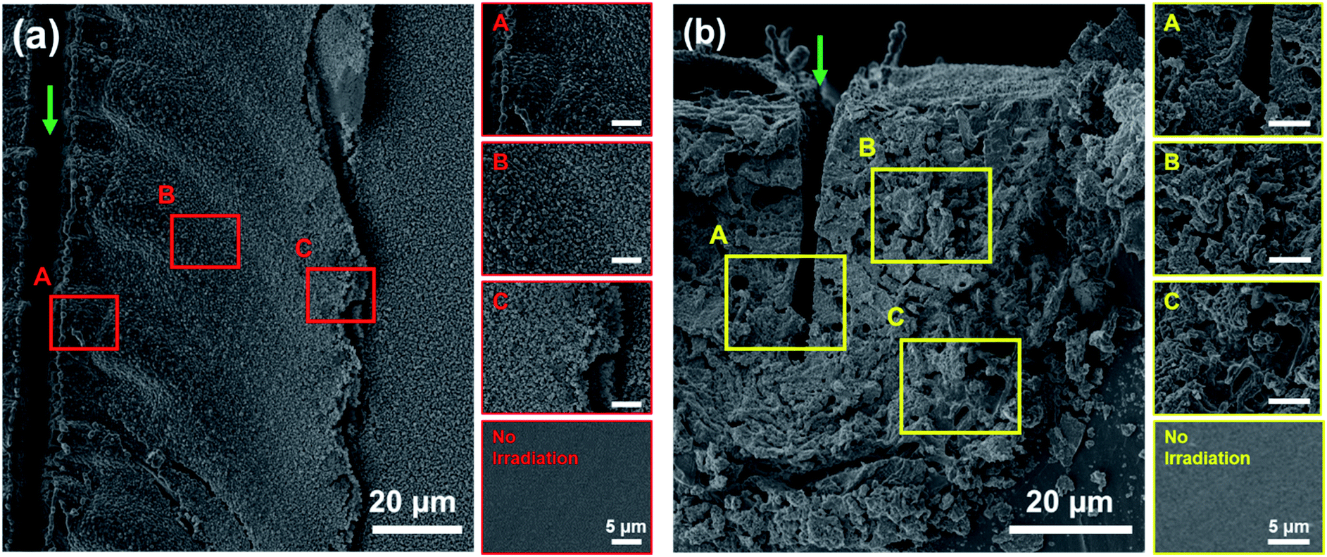 | ||
| Fig. 4 SEM images of the (a) surface, and (b) cross section of the fabricated line structure. A, B, and C are enlarged images of the respective locations. Structures were fabricated with laser power of 150 mW and scan speed of 2 mm s−1. Green arrow indicates the location of laser scanning. | ||
At location A in Fig. 4(b), the clean edge resulting from the ablation of the formed material is observed. Additionally, the modified region appears less porous, compared to other locations at the cross section. At location B in Fig. 4(b), the modified region is highly porous, and non-spherical masses are observed throughout the area. At location A, similar to the case on the surface, higher thermal effects may have melted and joined the neighboring masses, observed at location B, producing less-porous regions. At the boundary between the fabricated structure and the PDMS substrate, location C in Fig. 4(b), regions with considerably less surface roughness are observed. Such regions may be amorphous polymeric byproducts of the modification process, such as polycarbosilane (PCS), due to insufficient thermal effects at the edge.
3.3. Materials analyses of the modified region
Raman spectra were obtained at various locations of the line structure, fabricated with a laser power of 150 mW and scanning speed of 2 mm s−1, to investigate if the formed material was uniform throughout the modified region. Fig. 5 shows the Raman spectra of the surface (Fig. 5(a)) and cross section (Fig. 5(b)). From the Raman spectra obtained at locations A and B of the surface, peaks were observed at ∼1350 cm−1 and ∼1580 cm−1, while no peaks were observed at ∼2700 cm−1 (Fig. 5(a)). These peaks correspond to the D band (∼1350 cm−1), which reveals the formation of defects and bending of sp2 bonded carbons, the G band (∼1580 cm−1), which originates from the primary planar vibrational mode of the sp2 bonded carbons, and the 2D band (∼2700 cm−1), which results from the second-order lattice vibration mode, of graphitic carbon.18 From the fact that the D band is higher than the G band in the resulting Raman spectra for both A and B in Fig. 5(a), the formation of graphitic carbons containing large amounts of impurities and defects, such as graphene oxide, is implied. Additionally, it can be assumed that the amount of formed graphitic carbon was low for location A and B of the surface, since the background noise of the obtained spectra is substantial, indicating that the acquired signals of the D and G bands were weak. Contrary to the results at location A and B, no peaks were observed in the spectrum obtained at location C of the surface. Considering the results of the observed particle-like structures via SEM (location C of Fig. 4(a)), it can be expected that thermal effects were less at such distances compared to the focal point and, consequently, insufficient degradation of PDMS for the formation of graphitic carbon occurred at location C.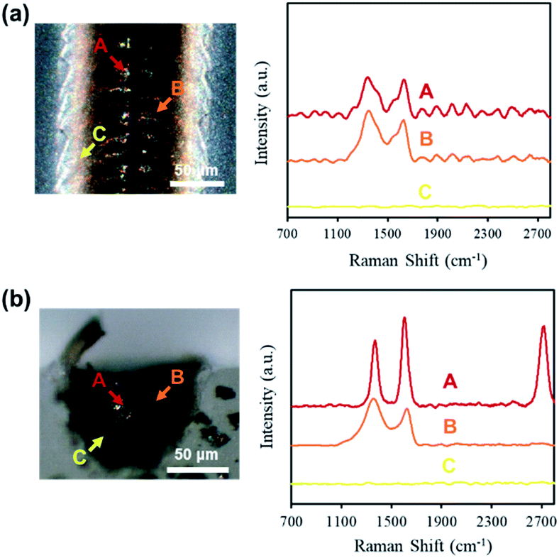 | ||
| Fig. 5 Raman spectra taken for different areas of the (a) surface, and (b) cross section. Structures were fabricated with laser power of 150 mW and scan speed of 2 mm s−1. Arrows indicate the location of analysis, and color of arrow corresponds to the color of the resulting Raman spectrum. | ||
From the spectra obtained at location A and B of the cross section, the observed D and G band peaks were significantly prominent compared to those of the surface (Fig. 5(b)). Moreover, the appearance of the 2D band was confirmed for the spectra obtained at location A. The Raman spectrum at location B implies the formation of graphitic carbons containing large amounts of impurities and defects, similar to that at location B of the surface. But since the peaks are smoother and the background noise is insignificant compared to the Raman spectrum obtained from location B of the surface, it can be deduced that the amount of graphitic carbon formed was higher for location B of the cross section. The Raman spectrum at location A implies the formation of multilayer graphitic carbon, with considerably fewer defects and impurities compared to location B. Considering the results of the observed particle-like structures via SEM (Fig. 4(b)), thermal effects are significantly higher near the focal spot, resulting in further degradation into graphitic carbon and, consequently, carbon materials with fewer defects at location A compared to B. The Raman spectrum obtained at C of the cross section is comparable to that of location C of the surface, indicating similar degradation at the edges of the surface and internally.
The Raman spectra obtained at the surface were significantly different from those at the cross section, and such dissimilarities may be due to the various conditions under which the degradation process occurs. For the modification processes occurring inside bulk PDMS, environmental factors, such as increased pressure and the absence of atmospheric gases, may have resulted in different products. For example, at the surface the presence of atmospheric oxygen can cause oxidation reactions, resulting in more oxidized products. Additionally, for the surface, nano-scale debris formed due to laser irradiation could precipitate and attach, resulting in a surface layer composed of non-carbon material.
For Raman spectra of the surface and cross section, no peaks were observed at ∼796 cm−1 and ∼972 cm−1, which correspond to the transverse (TO) and longitudinal optical (LO) vibrational modes of β-SiC.19
3.4. TEM observation of the fabricated structure
Submicron-scale analyses of the formed materials were conducted by TEM. TEM samples were prepared by removing specific areas of the line structure fabricated with a laser power of 150 mW and scanning speed of 2 mm s−1, indicated by the dashed green line in Fig. 6(a), using FIB. Fig. 6(b) shows a typical TEM image of the formed materials at location A. For the sample prepared from location A, monocrystalline structures, with an average grain size of approximately 50 nm, can be observed throughout the area. The inset in Fig. 6(b) shows the selected area electron diffraction (SAED) pattern of the field-of-view shown in Fig. 6(b). Clear spot-diffraction patterns can be observed, indicating the formation of highly crystalline nanoparticles.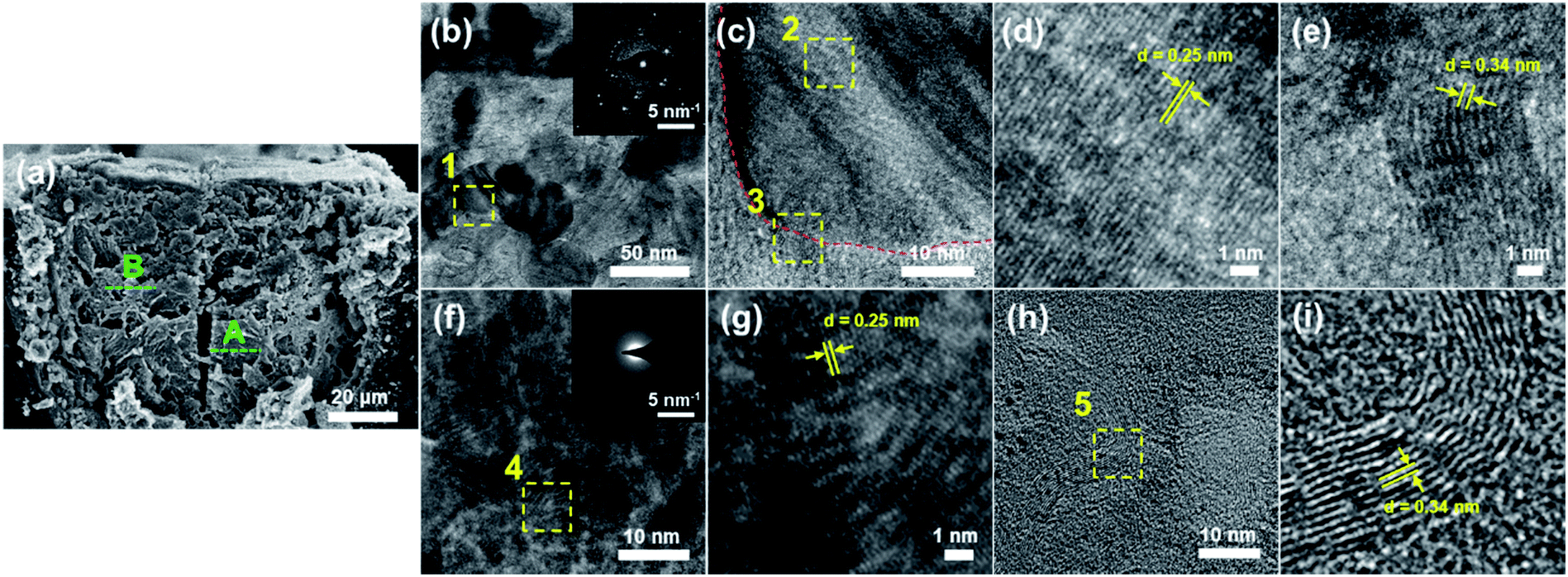 | ||
| Fig. 6 (a) SEM image showing the cross section of the analyzed structure. Structures were fabricated with laser power of 150 mW and scan speed of 2 mm s−1. Dashed green line indicates the location which TEM samples were prepared from: A (b–e) and B (f–i). (b) Typical TEM image of crystalline structures observed at A, and the inset is a corresponding SAED pattern of the observed area. (c) TEM image of the monocrystalline structure (indicated by the dashed red line) observed in area marked 1 in (b). (d, e) The enlarged images of the areas marked 2 and 3 in (c), respectively. (f) Typical TEM image of crystalline structures observed at B, and the inset is a corresponding SAED pattern of the observed area. (g) The enlarged images of the area marked 4 in (f). (h) TEM image of graphitic structures observed at a different area of B. (i) The enlarged images of the area marked 5 in (h). | ||
Fig. 6(c) shows a TEM image of the area marked 1 in Fig. 6(b). A monocrystalline structure, outlined by the dashed red line, can be observed in Fig. 6(c), and two distinctively different lattice fringes, marked 2 and 3, can be observed on and beside the structure, respectively. Furthermore, the materials observed in the area marked 3 seem to be sprouting from the edge of the monocrystalline structure, the area marked 2. Fig. 6(d) and (e) show enlarged images of the areas marked 2 and 3, respectively. In Fig. 6(d), lattice fringes with a spacing of approximately 0.25 nm were observed. This spacing corresponds to the (111) plane of β-SiC and, consistent with the previous reports by Nakajima et al.,17 the formation of crystalline SiC is indicated. Additionally, since the direction of the fringes is consistent throughout the observed monocrystalline structure, the observed structure is presumed to be a single nanoparticle of SiC. In Fig. 6(e), lattice fringes with a spacing of approximately 0.34 nm were observed. This spacing corresponds to the (002) plane of graphitic materials and, consistent with the Raman results, the formation of graphitic carbon is indicated.
Fig. 6(f) shows a typical TEM image of the formed materials at location B. Monocrystalline structures, similar to those observed at location A, were not observed for the sample prepared from location B. However, lattice fringes, distinctive of crystalline materials, can be observed throughout the field-of-view. The inset in Fig. 6(f) shows an SAED pattern of the field-of-view shown in Fig. 6(f). In contrast to the SAED patterns for location A, clear spot-diffraction patterns were not observed; instead halo-ring patterns, that reveal the formation of amorphous materials, were observed. Strong spot-diffraction patterns may not have been observed, regardless of the visible crystals, because the crystals formed in this location were thin and small for clear diffractions.
Fig. 6(g) shows an enlarged image of the area marked 4 in Fig. 6(f). Lattice fringes with a spacing of approximately 0.25 nm were also observed, indicating the formation of β-SiC at location B as well. However, the directions of the lattice fringes were diverse throughout the observed area, revealing the formation of various SiC nanoparticles facing different directions. Such observations suggest that an aggregation of crystalline SiC nanoparticles, with grain sizes of less than 10 nm, formed at location B. Furthermore, lattice fringes that correspond to graphitic carbon were not observed around the nanoparticles in this particular area (Fig. 6(f) and (g)), as was seen for location A. In a different area, lattice fringes, with a spacing consistent with that of graphitic materials (∼0.34 nm), were observed (Fig. 6(h) and (i)); although crystalline nanoparticles were not observed in this particular area. The difference in the heat effects between location A and B could account for the difference in the grain size. As observed via the TEM images, the SiC nanoparticles are covered by graphitic, as well as amorphous, materials. The existence of such materials around the nanoparticles may have hindered the excitation during the Raman analyses, similar to the study reported by Cao et al.20 What is particularly interesting is for location B, the SiC nanoparticles and graphene structures existed independent of one another, implying independent formation mechanisms for each material, and further investigation on the formation mechanism could allow for the selective fabrication of the desired material, as well as the control of features, such as grain size.
3.5. Electrical conductivity of the fabricated structures
Two-dimensional structures were fabricated by raster scanning femtosecond laser pulses (length: 4 mm), with a scan-to-scan distance of 50 μm, on the surface of PDMS. Structures were fabricated using a laser power of 150 mW, scanning speed of 2 mm s−1, and different numbers of scans. Assuming that the width of a single line structure fabricated with the above parameters is approximately 130 μm, according to the results of Fig. 2, each line structure fabricated with one scan had a ∼40% overlap with the adjacent line structure.Fig. 7(a)–(d) show the digital microscope images of the surface of the structures fabricated with 1 scan (Fig. 7(a)), 2 scans (Fig. 7(b)), 3 scans (Fig. 7(c)), and 10 scans (Fig. 7(d)), respectively. Laser pulses were raster scanned from the right side to the left side of the image. The surface modification of PDMS due to consecutive scanning (Fig. 7(b)–(d)) was visibly different from the modification due to single scanning (Fig. 7(a)). In the case of consecutive scanning, since the succeeding scan overlaps with the existing structure, various parameters, such as the absorption coefficient, thermal conductivity, and scattering coefficient, could change compared to the case of single scanning on PDMS.
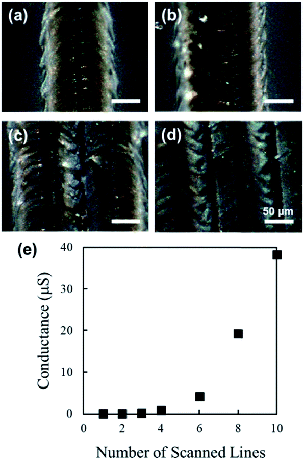 | ||
| Fig. 7 Digital microscope images showing the surface of structures fabricated with (a) 1 scan, (b) 2 scans, (c) 3 scans, and (d) 10 scans, respectively. Structures were fabricated with laser power of 150 mW, scan speed of 2 mm s−1, and line spacing of 50 μm. Laser pulses were raster scanned from the right side to left side. (e) Change in electrical conductance with respect to number of scanned lines. Electrical conductivity was measured for structures fabricated with 3 or more scans. | ||
Gold electrodes were fabricated on both ends of the 4 mm-long structures, with a 1 mm overlap on both ends, and the electrical resistance was measured using the two-probe method. Fig. 7(e) shows the calculated electrical conductance, using the measured electrical resistance, of the structures fabricated with various numbers of scans. No electrical conductance was confirmed for structures fabricated with one or two scans. On the contrary, structures fabricated with three and more scans indicated electrical conductivity, and the calculated electrical conductance increased exponentially with an increase in the number of scanned lines (Fig. 7(e)). The change in electrical conductance with the increase in the number of scanned lines could be explained by various factors, such as the increase in the cross-sectional area and further modification of the formed carbon structures due to the adjacent scanning.
3.6. Discussion of the change in conductance with scanning
The fabricated structures, shown in Fig. 7, were cut perpendicular to the laser scanning direction, and the cross sections were observed. Fig. 8(a)–(d) show the digital microscope images of the surface of the structures fabricated with 1 scan (Fig. 8(a)), 2 scans (Fig. 8(b)), 3 scans (Fig. 8(c)), and 10 scans (Fig. 8(d)), respectively. Laser pulses were raster scanned from the right side to the left side of the image. Periodic grooves that correspond to the scan-to-scan distance of 50 μm can be observed in the cross-sectional images (Fig. 8(b)–(d)).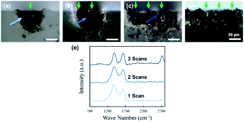 | ||
| Fig. 8 Digital microscope images showing the cross sections of structures fabricated with (a) 1 scan, (b) 2 scans, (c) 3 scans, and (d) 10 scans, respectively. Structures were fabricated with laser power of 150 mW, scan speed of 2 mm s−1, and line spacing of 50 μm. Laser was raster scanned from the right side to left side. Green arrow indicates the location of laser scanning. (e) Raman spectra taken for different areas of the cross sections. Arrows indicate the location of analysis, and color of arrow corresponds to the color of the resulting Raman spectrum. | ||
Analogous to the case of the surface, the modification of PDMS due to consecutive scanning (Fig. 8(b)–(d)) is visibly different to the modification due to single scanning (Fig. 8(a)). The area of modification resulting from the second scanning is clearly smaller than the case of single scanning (Fig. 8(b)). Less expansion of the modified region, both horizontally and vertically, was observed for the left side of the second groove. Since the second laser scanning overlaps with the existing line structure, laser pulses of the second scan will be absorbed by the formed carbon structures more than by the PDMS substrate. Furthermore, considering that carbon has significantly higher thermal conductivity than PDMS, the heat energy resulting from the second scan will dissipate towards the pre-existing structure, instead of radially towards the PDMS, resulting in significantly smaller modification regions. Consequently, the third scanning will be performed on the PDMS, since the modified region was not as wide for the second scanning (Fig. 8(c)). However, compared to the first scan an existing structure exists to the right side of the scan; therefore the modified region will not expand as much, although it will expand more than for the second scanning. The width of the modified region due to the third scanning is less than 100 μm; thus with a line spacing of 50 μm, the subsequent scans will not overlap with an existing structure. But, similar to the third scanning, the degree of outward expansion will be less than that of the first scanning, resulting in a shallower modification region, similar to that of the third scanning (Fig. 8(d)). Considering that the cross-sectional area did not increase exponentially, whereas the electrical conductivity did, the change in electrical conductance with the increase in the number of scanned lines cannot be interpreted with the change in cross-sectional area alone.
Fig. 8(e) shows the Raman spectra obtained for the cross sections for structures fabricated with various scans. Analysis, for each structure, was conducted on the area left of the groove formed due to the first scanning, indicated by the arrows in Fig. 8(a)–(c). A Raman spectrum, comparable to the spectrum obtained from location B in Fig. 5(b), was obtained from the structure fabricated with 1 scan. The spectrum obtained from the structure fabricated with 2 scans was roughly the same, indicating the formation of graphitic carbon with impurities and defects. However, the intensity ratio between the D and G peaks (ID/IG), which is often analysed to quantify disorder in graphene layers, changed from ∼1.4 to ∼1.2, indicating a decrease in impurities and/or defects of the structure fabricated by the first scanning due to the second scan. For the spectrum obtained from the structure fabricated with 3 scans, a further decrease in ID/IG (∼1.0), as well as the appearance of the 2D band was observed, indicating the evolution of the graphitic carbon into crystalline carbon. With successive raster scanning, the subsequent scans affect the existing structures and in-turn removes and repairs the existing impurities and defects. By continuing the raster scan process, it can be expected that the disorder in the graphene layers will be further decreased, resulting in the improvement of the crystallinity of the graphitic carbons, up to a certain distance from the laser focal spot. With the increase in laser scanning, the volume of such graphitic carbons with high crystallinity will increase, resulting in higher electrical conductivities. In this present study, no significant role of the SiC nanoparticles was observed. However, SiC is a wide-bandgap semiconductor used for various applications, such as high-powered electronic devices and sensors. With further investigation of the degradation mechanism, the selective fabrication of SiC and graphitic carbon could be realized, offering great potential for novel PDMS-based electronic devices.
4. Conclusions
The dimensions of the modified regions of PDMS, by femtosecond laser irradiation, changed depending on the laser power and scanning speed used for fabrication. Furthermore, the dimensions of all the structures fabricated were considerably larger than the focal diameter of the laser pulse, which is considered to be due to the thermal effects resulting from the high repetition rate. Analyses of the modified region showed the formation of SiC nanocrystals and graphitic carbon due to laser irradiation of PDMS; however, the features of the formed materials varied depending on the distance from the focal spot, which is attributable to higher photo-thermal effects near the focal spot. The Raman spectra indicated that the graphitic carbon formed closer to the focal spot contained significantly fewer defects and higher crystallinity. TEM observations confirmed the formation of SiC nanoparticles with different grain sizes, ranging from 50 nm to <10 nm, depending on the distance from the laser focal spot. Structures fabricated with varying numbers of raster scans showed an increase in electrical conductance with the increase in the number of scans. The Raman spectra of the structures indicated a decrease in disorder of the graphitic carbon with the increase in the number of scans, indicating the effect of the graphitic carbon, in particular the amount of disorder in the carbon lattice, on the electrical conductivity. By elucidating the degradation mechanism of PDMS to SiC and graphitic carbon, the selective fabrication of semiconducting and conducting materials and the precise control of the features of the formed material, such as grain size, could be realized, allowing tunable functionalization of PDMS for novel electronic device applications.Conflicts of interest
There are no conflicts to declare.References
- P. J. Scully, D. Jones and D. A. Jaroszynski, J. Opt. A: Pure Appl. Opt., 2003, 5, S92 CrossRef CAS.
- J. B. In, B. Hsia, J. Yoo, S. Hyun, C. Carraro, R. Maboudian and C. P. Grigoropoulos, Carbon, 2015, 83, 144–151 CrossRef CAS.
- A. Lamberti, F. Clerici, M. Fontana and L. Scaltrito, Adv. Energy Mater., 2016, 6, 1600050 CrossRef.
- S. Hayashi, Y. Nakajima and M. Terakawa, Opt. Mater. Express, 2019, 9, 6 Search PubMed.
- J. J. Kipling, J. N. Sherwood, P. V. Shooter and N. R. Thompson, Carbon, 1964, 1, 315–320 CrossRef CAS.
- M. Schumann, R. Sauerbrey and M. C. Smayling, Appl. Phys. Lett., 1991, 58, 428 CrossRef CAS.
- J. Lin, Z. Peng, Y. Liu, F. Ruiz-Zepeda, R. Ye, E. L. G. Samuel, M. J. Yacaman, B. I. Yakobson and J. M. Tour, Nat. Commun., 2014, 5, 5714 CrossRef CAS PubMed.
- N. Morita, Y. Shimotsuma, M. Nishi, M. Sakakura, K. Miura and K. Hirao, Appl. Phys. Lett., 2014, 105, 201104 CrossRef.
- Y. Zhu, H. Cai, H. Ding, N. Pan and X. Wang, ACS Appl. Mater. Interfaces, 2019, 11, 6195–6200 CrossRef CAS PubMed.
- S. Lee and S. Jeon, ACS Sustainable Chem. Eng., 2019, 7, 2270–2275 CrossRef CAS.
- K. E. Gonsalves and K. T. Kembaiyan, Solid State Ionics, 1989, 32/33, 661–668 CrossRef.
- K. E. Gonsalves, P. R. Strutt, T. D. Xiao and P. G. Klemens, J. Mater. Sci., 1992, 27, 3231–3238 CrossRef CAS.
- M. Suzuki, Y. Maniette, Y. Nakata and T. Okutani, J. Am. Ceram. Soc., 1993, 76, 1195–1200 CrossRef CAS.
- P. Colombo, A. Martucci, O. Fogato and P. Villoresi, J. Am. Ceram. Soc., 2001, 84, 224–226 CrossRef CAS.
- Y. Gao, Q. Li, R. Wu, J. Sha, Y. Lu and F. Xuan, Adv. Funct. Mater., 2019, 29, 1806786 CrossRef.
- K. Jakubenas and H. L. Marcus, J. Am. Ceram. Soc., 1995, 78, 2263–2266 CrossRef.
- Y. Nakajima, S. Hayashi, A. Katayama, N. Nedyalkov and M. Terakawa, Nanomaterials, 2018, 8, 558 CrossRef PubMed.
- M. S. Dressselhaus, A. Jorio, M. Hofmann, G. Dresselhaus and R. Saito, Nano Lett., 2010, 10, 751–758 CrossRef PubMed.
- S. Nakashima and H. Harima, Phys. Status Solidi A, 1997, 162, 39–64 CrossRef CAS.
- T. Cao, Y. Cheng, H. Zhang, B. Yan and Y. Cheng, J. Mater. Chem. C, 2015, 3, 4876–4882 RSC.
| This journal is © The Royal Society of Chemistry 2020 |