
 Open Access Article
 This Open Access Article is licensed under a Creative Commons Attribution-Non Commercial 3.0 Unported Licence
On-site growth method of 3D structured multi-layered graphene on silicon nanowires†
Steaphan Mark
Wallace
*ab,
Wipakorn
Jevasuwan
a and
Naoki
Fukata
 *ab
*ab
aInternational Center for Materials Nanoarchitectonics, National Institute for Materials Science, Tsukuba, 305-0044, Japan. E-mail: FUKATA.Naoki@nims.go.jp; steaphan.Wallace@gmail.com
bGraduate School of Pure and Applied Sciences, University of Tsukuba, Tsukuba, 305-8573, Japan
First published on 23rd March 2020
Abstract
An experimental method is described in which a orderly 3D array of graphene sheets is grown to conform to the shape of an underlying nanowire (NW) substrate that remains on-site. The procedure uses a sacrificial nickel catalyst-based CVD growth process that is capable of producing graphene onto an insulating SiO2 substrate. Nano-imprint silicon NWs serve both as the scaffolding for the catalyst and as the final underlying substrate. The graphene is polycrystalline and multi-layered as expected from this nickel catalyzed growth method. This presents a novel and quick method that can be used to produce conductive graphene sheets in precise shapes and configurations seen in complex device applications but which are difficult to produce with current transfer methods. The geometry of the nanostructured substrate itself contributes to the on-site growth method by making it difficult for the graphene to wash off during wet etching. The SiNWs used in this research have increased surface area and a light trapping effect that, in combination with the graphene, can be used in future sensor and photovoltaic device applications.
Introduction
Graphene is often discussed as being a two-dimensional material and many current methods of synthesizing graphene consequently rely on planar catalytic substrates. These flat catalysts are good for producing graphene sheets but the catalysts themselves are usually not the desired location for application. Various transfer methods are used to move the graphene to other device substrates, but this often reduces control and quality and takes more effort than if the graphene were produced on-site.1 Moreover, limiting graphene to flat configurations limits its potential applications and its ability to be incorporated into the current silicon device industry which often uses three-dimensional structures.2 Some forms of 3D graphene structures have been produced by various groups either using suspended graphene solutions or using 3D catalytic substrates.3–5 However, the final 3D graphene structures have been in random spatial orientations and are sometimes still bound to the original catalyst. Our group's goal was to develop continuous graphene sheets which can be grown in precisely controlled and orderly 3D configurations, which remain on-site after removal of the growth catalyst, and are compatible with silicon nanostructure technology. Through such a combination of attributes, variable control of the graphene shape and underlying substrate can lead to a diverse range of future research endeavours.There have been many early studies about chemical vapor deposition (CVD) growth of graphene on a nickel substrate which performs well as a catalyst both for breaking down the carbon precursors and for initiating graphene growth.6–9 It is explained that Ni absorbs carbon over time which then precipitates out as graphene during cooling, which can lead to multilayer structures depending on how much carbon was absorbed.9,10 The graphene can be seen to grow on many of the common Ni crystal planes but the growth dynamics and graphene thicknesses are different along the different planes.11,12 It can be especially difficult to control the growth on the different Ni crystal planes of a multi-crystalline or complex-shaped Ni surface to meet the demand for thin graphene. However, Ni was selected in this experiment as it is easy to deposit over a 3D structure, it has a suitable thin-film melting point and because of its compatibility with the severe growth conditions used here. Whereas similar previous experiments have used thicker, planar Ni substrates annealed over long periods of several minutes,13–15 this experiment necessitated a very thin Ni film which has increased dewetting behavior at high temperatures.16 To compensate, the annealing times used here are very rapid and other experimental parameters are adjusted accordingly.
To accomplish the 3D objective of this experiment, an orderly array of nano-imprint silicon nanowires (SiNWs) were used as the base substrate. The deposited nickel conforms to the shape of the NWs, allowing the graphene to be grown in the same configuration. Nanoimprint NWs were chosen to showcase the process because of their controllable shape and orientation. It is desirable that the graphene will remain on this nanostructure surface after growth and after removal of Ni, meaning the destructive chemical interaction between Ni and Si which produces nickel silicide17 must be avoided by the use of a passivation layer. For this current experiment, a SiO2 thin film was used to protect the Si and to act as an insulating layer for future characterization.
Experimental
Silicon NWs in well-ordered 1 cm2 arrays were prepared by nanoimprint lithography onto 2.25 cm2 n-type Si wafer squares.18 Standard samples had NWs with lengths of 500 nm and diameters of 200 nm at 600 nm intervals. Samples were cleaned in acetone, isopropanol, and DI-water for 10 minutes each. SiO2 thin films were produced on the Si surface by annealing the SiNWs in an oxygen-rich atmosphere at 975 °C at atmospheric pressure. A SiO2 thickness of about 70 nm was typically used but thicknesses down to 35 nm could also be successfully used in this experiment. Ni was deposited on samples under rotation using a Shibaura Mechatronics sputtering machine for a thickness of 200 nm on flat perpendicular surfaces. Planar silicon substrates without nanowires were also treated with the same procedures to serve as control samples.An outline of the process of graphene formation on SiNWs is shown in Fig. 1. Immediately before annealing, the samples were cleaned using 10 vol% HCl![[thin space (1/6-em)]](https://www.rsc.org/images/entities/char_2009.gif) :H2O for 1 minute for the purpose of removing nickel oxide, then washed in ethanol and DI-water. The samples were then placed in a quartz boat in the cool zone of a custom-made hot-walled quartz tube furnace (Fig. S1†) which was heated to 875 °C and stabilized. The atmosphere was removed and 100 sccm He: 30 sccm CH4 was introduced and held at 400 torr. Then, the samples were annealed by quickly placing them in the furnace hot zone for approximately 1.5 minutes, then quickly moved back to the cool zone to allow the samples to return to room temperature. Note that the very short annealing time means that the samples spent most of this time heating to the target temperature as depicted in Fig. 1(b) and that the required time depends partly on the size of the sample. To remove the Ni catalyst, the cooled samples were etched in Marble's reagent (1 g CuSO4:5 ml HCl:5 ml H2O) for 2 minutes and washed in DI water.
:H2O for 1 minute for the purpose of removing nickel oxide, then washed in ethanol and DI-water. The samples were then placed in a quartz boat in the cool zone of a custom-made hot-walled quartz tube furnace (Fig. S1†) which was heated to 875 °C and stabilized. The atmosphere was removed and 100 sccm He: 30 sccm CH4 was introduced and held at 400 torr. Then, the samples were annealed by quickly placing them in the furnace hot zone for approximately 1.5 minutes, then quickly moved back to the cool zone to allow the samples to return to room temperature. Note that the very short annealing time means that the samples spent most of this time heating to the target temperature as depicted in Fig. 1(b) and that the required time depends partly on the size of the sample. To remove the Ni catalyst, the cooled samples were etched in Marble's reagent (1 g CuSO4:5 ml HCl:5 ml H2O) for 2 minutes and washed in DI water.
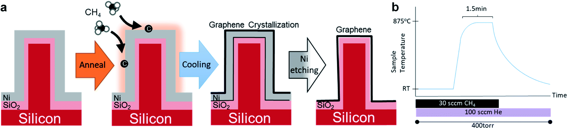 | ||
| Fig. 1 (a) Proposed process outline of Ni on SiO2 on SiNWs annealed at 875 °C with CH4 to deposit carbon and form a graphene sheet. The Ni is etched with Marble's reagent to leave the graphene directly on the NWs. (b) Schematic depicting the standard experimental growth conditions of graphene on the 2.25 cm2 NWs substrate. | ||
Imaging of the samples was conducted by scanning electron microscope (Hitachi SU8000 FE-SEM) at 5 kV, and by transmission electron microscope (JEOL JEM-2100 200kV-TEM/EDS). Energy dispersive spectroscopy was performed using the above SEM and TEM systems. Vibrational spectroscopy for molecular analysis was conducted using a Raman micro-spectrometer with a 532 nm laser source and a 100× magnification lens.
Results & discussion
Standard-sample characterization
SEM was used extensively to keep track of the structural conditions and changes in the sample throughout the process.19 The nanoimprinted NWs as shown in Fig. 2(a) had smooth walls, flat tops and enough room in-between to allow the sputtered Ni to produce a smooth, dense, and mostly uniform-thickness film as seen in Fig. 2(b). The thickness of the Ni is highest on the NW tops and decreases going down the side-walls due to the nature of the sputtering. Despite the short annealing times, the thin Ni film reaches a temperature in which grain growth occurs, the surface smooths out as seen in Fig. 2(c), and the beginnings of hole nucleation leading to dewetting can be observed. If the temperature is too high or held for too long, the Ni thin film will continue to dewet from the surface and disrupt proper graphene formation. The annealing temperature and time are critical in determining the final state of the Ni and therefore the graphene at the time of cooling down.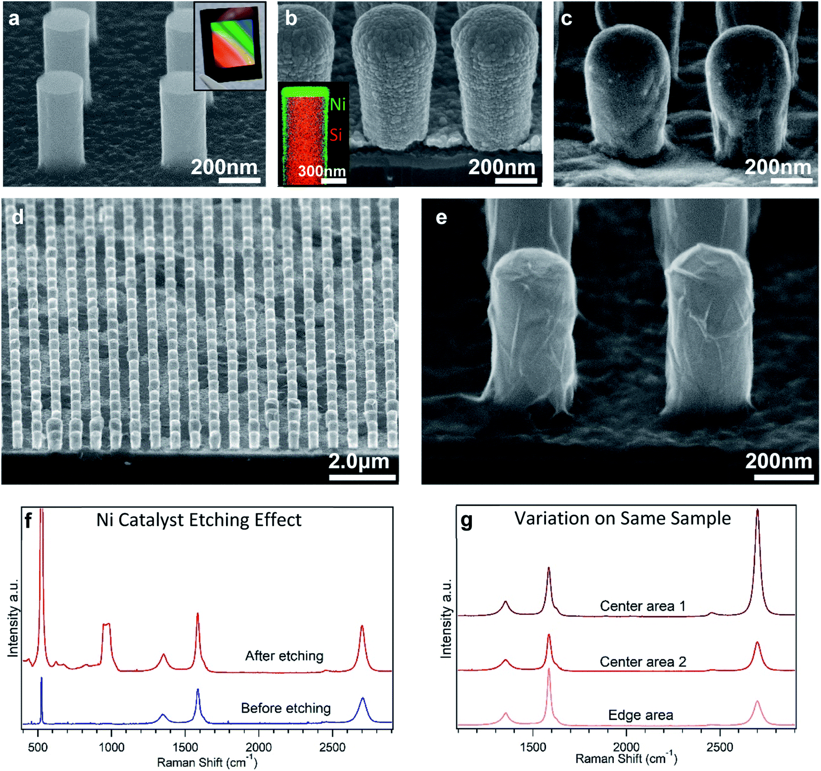 | ||
| Fig. 2 (a) SEM image of evenly spaced SiNWs at 600 nm periods and inset photo of the entire sample. (b) Ni deposit on 500 nm period NWs (and inset TEM-EDS map of Ni on larger NW to emphasize the thinner coating on the sides) (c) sample annealed with CH4 for 1.5 min. (d) The sample is etched to remove Ni and leave a graphene layer over a large area and (e) continuous over the NW and floor surfaces as made visible by the presence of wrinkles, seen here on a severed edge. (f) Raman spectra of NWs before and after Ni etching. The Si peaks, mainly at 520 cm−1 and 960 cm−1 are suppressed by the Ni and revealed after etching. The carbon D, G, and 2D peaks at 1350 cm−1, 1580 cm−1, and 2700 cm−1 respectively remain similar before and after etching and suggest a multi-layered strained graphene structure. (g) NWs from the same sample at random locations showing different G:2D peak ratios and thereby a variation of graphene layering. The bottom spectrum is from the sample edge. | ||
After Ni is etched away, SEM observations in Fig. 2(d and e) show that the SiNWs are left mostly intact but are now clearly covered with sheets that extend over the NWs and the bottom substrate surface between them. The sheets are darker in contrast than the underlying insulative SiO2 substrate as expected for multilayer graphene20 while the NWs themselves appear bright due to topography effects.21 The sheet is continuous from one NW to another and covers the entire NW sample array. It is also loose in appearance and often includes wrinkles though it appears to be in contact with the NW surface. The size and shape of the visible sheets are similar to the Ni layer's outer dimensions and suggests that it originated from the top surface of the Ni.
Raman spectra from both before and after Ni etching show similar peaks at around 1350 cm−1, 1580 cm−1, and 2700 cm−1 corresponding to carbon D, G, and 2D peaks respectively. The strong G and 2D peaks are indicative of the presence of graphene.22–25 For the bottom spectrum in Fig. 2(f), Ni is still present on the sample surface and while Ni does not have a Raman signature it does have the effect of dampening the Si peaks at 520 cm−1 and 960 cm−1 which are then revealed in the upper spectrum of Fig. 2(f) after the nickel is removed. Conversely, the carbon peaks do not change significantly in peak ratio or intensity after the nickel is removed, showing that the graphene is not considerably altered by the etching process and probably exists on the outer surface of the nickel.
The size ratio between the G and 2D peaks roughly corresponds to the degree of layering of the graphene and the ratios seen here would indicate a few layers of graphene. The 2D peak intensity does have some random variation between sample locations as seen in Fig. 2(g), with particularly small 2D peaks along the substrate edges as these areas are expected to have different temperature conditions in our furnace setup. The carbon D peak is often attributed to defects or edges in the graphene crystal structure. Unlike the 2D peak, the clear D peak in these samples tends to be a consistent size over the whole sample and its cause is of interest for future analysis.
TEM analysis was performed to confirm the formation of graphene layers after nickel removal. Scans of the surfaces of mechanically severed NWs have produced images of carbon sheets resting directly on the NWs as in Fig. 3(a). Individual graphene layers can be seen in Fig. 3(b) as the dark stacked lines with 0.34 nm inter-layer spacing which is expected of stacked graphene layers.26,27 Often around 8 or more layers can be observed with this TEM method, and the number varies from place to place. This kind of multi-layered and polycrystalline structure can be expected from CVD grown graphene on polycrystalline Ni and with high hydrocarbon exposure.6,28 Additionally, both TEM energy dispersive spectroscopy (EDS) of single NWs and SEM-EDS spectra over wide sample areas after etching do not display Ni peaks, indicating that the nickel is effectively removed from the sample after etching as seen in Fig. 3(c), S2 and S3.†
 | ||
| Fig. 3 (a) TEM image of single NW mechanically severed from the sample and still covered with multilayer graphene. (b) TEM image showing multilayers with 0.34 nm spacing corresponding to graphene directly on the SiO2 surface. (c) SEM-EDS of multiple NWs after etching shows that no or negligible Ni remains on the surface. | ||
Thick Ag on Ti electrodes were deposited onto the sample corners to conduct a simple four-probe van der Pauw sheet resistance test to see if the sheet connects over the entire sample. Values of around 450 Ω per square were produced which is consistent with other reports of the sheet resistance of un-doped graphene.29 However, as the probes can break the SiNWs during testing, possible contribution of the underlying silicon substrate to this value cannot be disregarded.
Nickel behavior
As already mentioned, the dewetting behavior of Ni is both a point of difficulty and interest in this experiment. As this behavior had a dominant influence on the results, the effects of temperature, annealing time and deposition thickness on the Ni thin film were preliminarily examined. Although Ni sputtering here produces a thickness of 200 nm on flat, perpendicular surfaces, the Ni layer is thinner along the NW sides and can be as thin as 50 nm at the base of the NWs. The melting temperature is therefore drastically reduced from the bulk melting temperature of 1455 °C. Tests of this Ni thickness at 775 °C showed no signs of melting or grain growth, while heating to 850 °C and higher eventually shows destructive dewetting and migration behavior over long enough time periods. For the 2.25 cm2 sample areas, a time of 1 minute 30 seconds had minimal dewetting while a time of 2 minutes or more showed extensive dewetting and reduced surface quality. Altering the Ni thickness will change these temperature findings, and this was seen in the experiment as well. When the Ni thickness was reduced to 65 nm on flat perpendicular surfaces, nickel dewetting was seemingly unavoidable at high enough temperatures required for this type of CVD graphene formation, as seen in Fig. 4(a).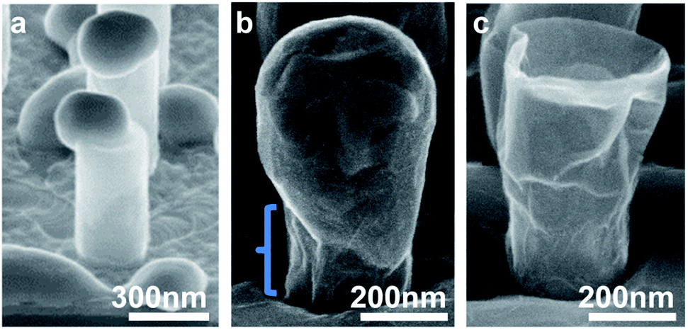 | ||
| Fig. 4 (a) 65 nm Ni deposit showing drastic dewetting behaviour after annealing (b) Graphene formed during annealing is visible on the exposed SiO2 after partial dewetting and migration of Ni that (c) when etched forms a sheet over the entire NW and which is larger at the top because of the shape of the dewetted Ni. | ||
Despite the very rapid growth conditions, thick graphene sheets and high coverage could be seen and so the graphene growth pattern was also a point of interest. A typical explanation of graphene growth on the Ni surface at high temperature describes carbon absorption into the nickel during annealing and carbon precipitation back to the surface during cooling, especially from grain boundaries.30 However, the amount of absorption might be limited in this short of annealing time. In our experiments, Ni dewetting and migration at high temperature can leave gaps in the Ni layer as seen in Fig. 4(b), but graphene layers can still be seen bridging over the gaps where Ni was presumably not present during cooling such as in Fig. 4(c). This implies that part of the graphene was grown while at high temperature before dewetting and not entirely during cooling. One explanation is that the carbon absorption was at such a high rate as to lead to immediate saturation and subsequent graphene growth from high enough hydrocarbon exposures.
Dependency on growth conditions
Following the observations at standard conditions, a systematic series of samples grown under various conditions were compared to find the best conditions and outline the effects of variables. All other variables were kept at the standard values as described in the experimental section. The Raman spectrum results are shown in Fig. 5. When the temperature was held at the standard 875 °C the Raman peak quality is good, while at 900 °C there is a noticeable decrease in quality. In SEM such as in Fig. 5(h) and S4† it can be seen that, in addition to the expected dewetting behavior, the Ni damages some of the SiO2 substrate material at 900 °C which is clearly detrimental to the NW quality. Therefore, 875 °C represents a near maximum temperature in which dewetting could be avoided for the amount of time required to form a graphene layer on this thin of Ni. Lowering the temperature to 850 °C did not significantly alter the Raman peak quality while its appearance in SEM in Fig. S5† is similar to that at 875 °C but with more areas of varying contrast.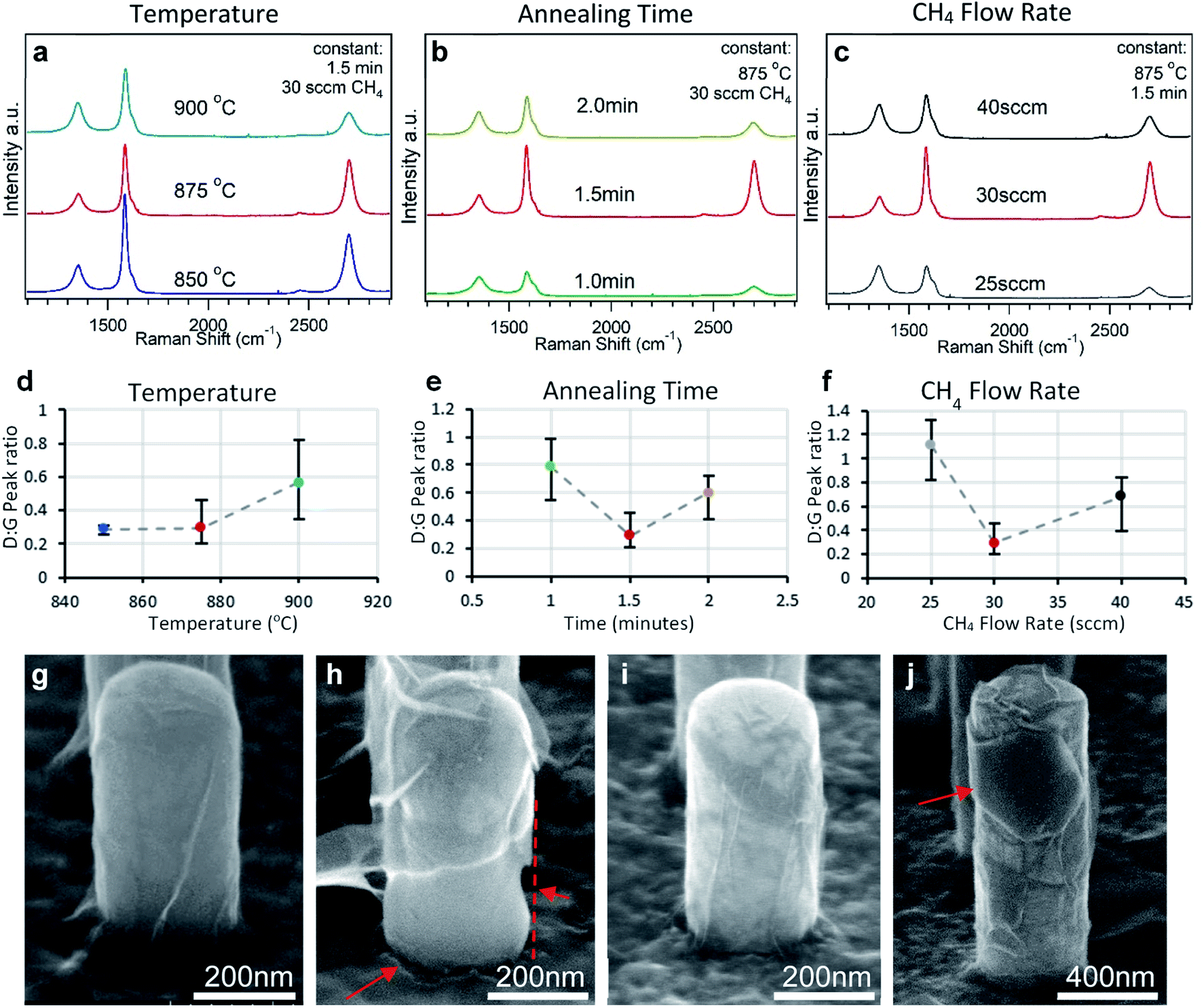 | ||
| Fig. 5 (a–c) Raman spectra of different samples synthesized at different variable values as listed. (d–f) Corresponding variable effects on the average carbon D:G Raman peak height ratio. Bars represent maximums and minimums. (g) SEM image of sample at standard conditions with homogeneous graphene appearance (h) SEM image of sample annealed at 900 °C and showing signs of SiO2 damage, an effect seen whenever Ni dewets. (i) Sample annealed for 1 minute with thin graphene sheet and various contrast, an effect also seen with low temperature, and low CH4 flow rate. (j) Large NWs displaying a thick section of multi-layered graphene with hexagonally shaped edges. | ||
When annealing time was increased to 2 minutes (at 875 °C) the same SiO2 damage caused by the Ni and subsequent loss in quality could again be seen in the Raman spectrum and SEM (Fig. S6†). The similarity of the SiO2 damage with the 900 °C sample leads us to believe that the damage occurs following Ni dewetting, under whichever conditions that this may occur. Conversely, a shorter time of 1 minute also had worse Raman peak quality and the carbon film observed by SEM (Fig. 5(i) and S7†) appears to be undefined with areas of varying contrast that indicate small patches of different layer thicknesses20,31 and which points to either incomplete growth and small domains or folding. Therefore, the annealing time of 1.5 minutes was used as a compromise and outlines the importance of finding the right time in this process.
CH4 concentration was controlled by the ratio of its flow rate with the carrier gas He flow rate of 100 sccm. Due to the short annealing time, relatively high ratios of 30 sccm of CH4 were necessary to increase growth rates. In samples that were annealed in the same process but with an increased flow rate of 40 sccm CH4, thick rigid films that could be peeled off the sample were produced (Fig. S8†). For lower rates of 25 sccm CH4, a thin film with patches of different contrast is seen in SEM (Fig. S9†) and the Raman spectrum quality was significantly reduced similar to that seen with the shorter annealing time, and it is thought that the reduced carbon exposure leads to similar incomplete graphene sheet formation. Likewise, lowering the chamber pressure to 50 torr also caused incomplete graphene growth as well as Ni dewetting leading to poor Raman peak results and fragmented graphene (Fig. S10†).
Dependency on NW architecture
It was found that the dimensions of the NWs also had some influence on the final properties of the graphene sheets. The dimensions of the NWs presented in the results above have a diameter of 200 nm, height of 500 nm, and are spaced at 600 nm intervals. When the NW diameter was increased to 400 nm and therefore the radius of curvature of the NW walls was increased, darker and therefore thicker hexagonal patches of graphene with sharp edges and corners with ∼120° angles were often seen on the NW walls and on the planar sections of the sample such as in Fig. 5(j). These patches seemingly correspond to the Ni (111) surface and are possibly due to the growth of large Ni crystal facets on the broad surfaces of the larger NWs and planar floors. Reducing the NW dimensions consequently has an effect of suppressing the formation of large Ni crystal surface planes which lead to the inhomogeneity problem seen on CVD graphene grown on polycrystalline Ni. On the other hand, when reducing the distance between NWs from 600 nm to 500 nm and increasing the NW length from 500 nm to 700 nm, the Ni was more likely to migrate away from the bases of the NWs due to the difficulty of sputtering Ni between these NWs (Fig. S11†). Therefore, small diameter and sufficiently spaced NWs produces the best results.Lastly, the NW configuration proved to be critical for the on-site growth properties. Experiments using the same conditions on both planar SiO2 thin-film Si substrates and pyramidal textured surfaces could successfully form graphene sheets, but wet-etching the Ni caused the graphene sheets to detach and float on the etching solution (Fig. S12†). This occurrence is not unusual as the same behavior is sometimes used to transfer graphene off of flat catalysts and onto other substrates by scooping.13,32 In contrast, the graphene on the NWs does not exhibit this behavior even while the flat sections around the NWs detach and rip off (Fig. S13†). This is proposed to be a result of the geometry of the NWs causing counter forces to horizontal movement and the difficulty of the graphene to be pulled up and off of multiple NWs both simultaneously or sequentially. We see that these complex structures can thereby be used in this way to secure the graphene onto the substrate that it was originally grown on.
Conclusions
In this research, a process for extending the mechanism of Ni catalyst-based CVD graphene synthesis onto the 3D surface of NWs was outlined and the experimental results were described. This process was successfully able to produce a continuous carbon sheet with graphene signatures and NW shape on the entire NW sample surface. This shows that graphene sheets can be produced with various nanostructures if the right growth conditions are found. The final architecture is not random but is orderly, repetitive, and controllable over a large area.The quality of the graphene produced in this experiment was multi-layered and therefore may be appropriate for use as a conductive layer. Although single-layer graphene is often sought after, this is likely to be difficult to obtain with a Ni substrate, even with short growth times. Moreover, the hot-walled furnace system described here, though sufficient for our experiment's purpose, acted as a limitation on the control of temperature, annealing time, and the introduction of gases. With the Ni catalyst's sensitivity to high temperatures over time, a more direct heating approach and observation of the true sample temperature would likely improve the results.
An exposed Si surface could not be used as it will react with the Ni, so it is necessary to use a passivation layer between the Si and the Ni during annealing. The passivation layer that was used for this experiment was SiO2 because it electrically isolates the graphene which aids characterization. Applications of this structure may include contacts and leads that have been shaped for complex surfaces and grown on-site by using NWs to anchor flat sheets. The NW configuration shown here increases the surface area of the graphene sheet and may be used for improved sensor applications. The silicon NWs themselves also have a light-trapping property which can be used to improve the absorption properties of light collecting devices.33 By removing the SiO2 layer after graphene growth, or by using an alternative passivation material, a graphene-based Schottky junction device is envisioned for photodetector or solar cell applications. Such a NW configuration could help to decrease the high absorption loss issue of equivalent planar graphene–silicon photovoltaic devices while increasing the interface area.34 Future experiments using alternative substrate layers and catalyst materials are being investigated in our laboratory.
This experiment has been a starting point for exploring the flexibility of graphene's ability to be grown in pre-arranged 3D configurations and in combination with other nanostructured material technology. The two-dimensionality of graphene has been one of its greatest characteristics, but by synthesizing it and retaining it in precise non-flat configurations we can expand its range of properties and its capability to be produced for future applications.
Conflicts of interest
There are no conflicts to declare.Acknowledgements
This work was supported by the World Premier International Research Center Initiative (WPI Initiative), MEXT, Japan. Training and support for the laboratory equipment used for this experiment was kindly given by Thiyagu Subramani. SiNWs were produced at the NIMS Nanofabrication Platform facilities. Sputtering, SEM, and TEM analysis was performed at the NIMS Namiki Foundry facilities.References
- J. Kang, D. Shin, S. Baea and B. Hee Hong, Graphene transfer: key for applications, Nanoscale, 2012, 4, 5527–5537 RSC.
- K. Kim, J.-Y. Choi, T. Kim, S.-H. Cho and H.-J. Chung, A role for graphene in silicon-based semiconductor devices, Nature, 2011, 479, 338 CrossRef PubMed.
- Z. Chen, W. Ren, L. Gao, B. Liu, S. Pei and H.-M. Cheng, Three-dimensional flexible and conductive interconnected graphene networks grown by chemical vapour deposition, Nat. Mater., 2011, 10, 424–428 CrossRef PubMed.
- J. Li, N. V. Toan, Z. Wang and T. Ono, Metal-assisted-chemical-etching of silicon nanowires for templating 3D graphene growth towards energy storage in microsystems, J. Micromech. Microeng., 2019, 29, 055007 CrossRef.
- M. Park, S.-K. Ahn, S. Hwang, S. Park, S. Kim and M. Jeon, Synthesis of Nitrogen-Doped Graphene on Copper Nanowires for Efficient Thermal Conductivity and Stability by Using Conventional Thermal Chemical Vapor Deposition, Nanomaterials, 2019, 9, 984 CrossRef.
- M. Batzill, The surface science of graphene: Metal interfaces, CVD synthesis, nanoribbons, chemical modifications, and defects, Surf. Sci. Rep., 2012, 67, 83–115 CrossRef.
- A. Dahal and M. Batzill, Graphene–nickel interfaces: a review, Nanoscale, 2014, 6, 2548–2562 RSC.
- G. Odahara, S. Otani, C. Oshima, M. Suzuki, T. Yasue and T. Koshikawa, In-situ observation of graphene growth on Ni(111), Surf. Sci., 2011, 605, 1095–1098 CrossRef.
- X. Li, W. Cai, L. Colombo and R. S. Ruoff, Evolution of Graphene Growth on Ni and Cu by Carbon Isotope Labeling, Nano Lett., 2009, 9, 4268–4272 CrossRef.
- J. C. Shelton, H. R. Patil and J. M. Blakely, Equilibrium segregation of carbon to a nickel (111) surface: A surface phase transition, Surf. Sci., 1974, 43, 493–520 CrossRef.
- J. M. Blakely, J. S. Kim and H. C. Potter, Segregation of Carbon to the (100) Surface of Nickel, J. Appl. Phys., 1970, 41, 2693–2697 CrossRef.
- M. Eizenberg and J. M. Blakely, Carbon interaction with nickel surfaces: Monolayer formation and structural stability, J. Chem. Phys., 1979, 71, 3467–3477 CrossRef.
- K. S. Kim, Y. Zhao, H. Jang, S. Y. Lee, J. M. Kim, K. Kim and J.-H. Ahn, Large-scale pattern growth of graphene films for stretchable transparent electrodes, Nature Lett., 2009, 457, 706 CrossRef.
- Z. Peng, Z. Yan, Z. Sun and J. M. Tour, Direct Growth of Bilayer Graphene on SiO2 Substrates by Carbon Diffusion through Nickel, ACS Nano, 2011, 5, 8241–8247 CrossRef.
- D. Q. McNerny, B. Viswanath, D. Copic, F. R. Laye, C. Prohoda, A. C. Brieland-Shoultz, E. S. Polsen, N. T. Dee, V. S. Veerasamy and A. J. Hart, Direct fabrication of graphene on SiO2 enabled by thin film stress engineering, Sci. Rep., 2014, 4, 5049 CrossRef.
- D. G. Gromov, G. P. Zhigal’skii, A. V. Karev, I. A. Karev, I. S. Chulkov and S. S. Shmelev, Fluctuation Phenomena in Nanoscale Nickel Films Near the Melting Point, Semiconductors, 2011, 45, 1689–1693 CrossRef.
- K.-N. Tu, E. I. Alessandrini, W. K. Chu, H. Krautle and J. W. Mayer, Epitaxial Growth of Nickel Silicide NiSi2, Jpn. J. Appl. Phys., 1974, 13, 669 CrossRef.
- K. J. Morton, G. Nieberg, S. Bai and S. Y. Chou, Wafer-scale patterning of sub-40 nm diameter and high aspect ratio (>50:1) silicon pillar arrays by nanoimprint and etching, Nanotechnology, 2008, 19, 345301 CrossRef.
- J. Lee, X. Zheng, R. C. Roberts and P. X.-L. Feng, Scanning electron microscopy characterization of structural features in suspended and non-suspended graphene by customized CVD growth, Diamond Relat. Mater., 2015, 54, 64–73 CrossRef.
- V. Kochat, A. N. Pal, E. S. Sneha, A. Sampathkumar, A. Gairola, S. A. Shivashankar, S. Raghavan and A. Ghosh, High contrast imaging and thickness determination of graphene with in-column secondary electron microscopy, J. Appl. Phys., 2011, 110, 014315 CrossRef.
- Y. Leng, Materials Characterization: Introduction to Microscopic and Spectroscopic Methods, Wiley-VCH, Germany, Weinheim, 2013 Search PubMed.
- A. C. Ferrari, J. C. Meyer, V. Scardaci, C. Casiraghi, M. Lazzeri, F. Mauri, S. Piscanec, D. Jiang, K. S. Novoselov, S. Roth and A. K. Geim, Raman Spectrum of Graphene and Graphene Layers, Phys. Rev. Lett., 2006, 97, 187401 CrossRef.
- A. C. Ferrari, Raman spectroscopy of graphene and graphite: Disorder, electron–phonon coupling, doping and nonadiabatic effects, Solid State Commun., 2007, 143, 47–57 CrossRef.
- L. M. Malard, M. A. A. Pimenta, G. Dresselhaus and M. S. Dresselhaus, Raman spectroscopy in graphene, Phys. Rep., 2009, 473, 51–87 CrossRef.
- A. C. Ferrari and D. M. Basko, Raman spectroscopy as a versatile tool for studying the properties of graphene, Nat. Nanotechnol., 2013, 8, 235 CrossRef.
- G. E. Bacon, The Interlayer Spacing of Graphite, Acta Crystallogr., 1951, 4, 558–561 CrossRef.
- M. Endo, K. Takeuchi, T. Hiraoka, T. Furata, T. Kasai, X. Sun, C.-H. Kiang and M. S. Dresselhaus, Stacking Nature of Graphene Layers in Carbon Nanotubes and Nanofibres, J. Phys. Chem. Solids, 1997, 58, 1707–1712 CrossRef.
- Y. Zhang, L. Gomez, F. N. Ishikawa, A. Madaria, K. Ryu, C. Wang, A. Badmaev and C. Zhou, Comparison of Graphene Growth on Single-Crystalline and Polycrystalline Ni by Chemical Vapor Deposition, J. Phys. Chem. Lett., 2010, 1, 3101–3107 CrossRef CAS.
- G. Jo, M. Choe, S. Lee, W. Park, Y. H. Kahng and T. Lee, The application of graphene as electrodes in electrical and optical devices, Nanotechnology, 2012, 23, 112001 CrossRef.
- L. Baraton, Z. B. He, C. S. Lee, C. S. Cojocaru, M. Chatelet, J.-L. Maurice, Y. H. Lee and D. Pribat, On the mechanisms of precipitation of graphene on nickel thin films, Europhys. Lett., 2011, 96, 46003 CrossRef.
- H. Hiura, H. Miyazaki and K. Tsukagoshi, Determination of the Number of Graphene Layers: Discrete Distribution of the Secondary Electron Intensity Stemming from Individual Graphene Layers, Appl. Phys. Express, 2010, 3, 095101 CrossRef.
- W. Liu, C.-H. Chung, C.-Q. Miao, Y.-J. Wang, B.-Y. Li, L.-Y. Ruan, K. Patel, Y.-J. Park, J. Woo and Y.-H. Xie, Chemical vapor deposition of large area few layer graphene on Si catalyzed with nickel films, Thin Solid Films, 2010, 518, S128–S132 CrossRef.
- W. Jevasuwan, K. Nakajima, Y. Sugimoto and N. Fukata, Metal-catalyzed electroless etching and nanoimprinting silicon nanowire-based solar cells: Silicon nanowire defect reduction and efficiency enhancement by two-step H2 annealing, Jpn. J. Appl. Phys., 2016, 55, 065001 CrossRef.
- X. Kong, L. Zhang, B. Liu, H. Gao, Y. Zhang, H. Yan and X. Song, Graphene/Si Schottky solar cells: a review of recent advances and prospects, RSC Adv., 2019, 9, 863–877 RSC.
Footnote |
| † Electronic supplementary information (ESI) available. See DOI: 10.1039/d0na00098a |
| This journal is © The Royal Society of Chemistry 2020 |