
 Open Access Article
 This Open Access Article is licensed under a Creative Commons Attribution-Non Commercial 3.0 Unported Licence
Anisotropic properties of pipe-GaN distributed Bragg reflectors
Chia-Jung
Wu
a,
Yi-Yun
Chen
a,
Cheng-Jie
Wang
a,
Guo-Yi
Shiu
a,
Chin-Han
Huang
a,
Heng-Jui
Liu
*a,
Hsiang
Chen
 b,
Yung-Sen
Lin
c,
Chia-Feng
Lin
*a and
Jung
Han
*d
b,
Yung-Sen
Lin
c,
Chia-Feng
Lin
*a and
Jung
Han
*d
aDepartment of Materials Science and Engineering, Innovation and Development Center of Sustainable Agriculture, Research Center for Sustainable Energy and Nanotechnology, National Chung Hsing University, Taichung, 145 Xingda Rd., South Dist., Taichung 402, Taiwan. E-mail: hengjui0109@dragon.nchu.edu.tw; cflin@dragon.nchu.edu.tw
bDepartment of Applied Materials and Optoelectronic Engineering, National Chi Nan University, No.1, University Rd., Puli Township, Nantou 545, Taiwan
cDepartment of Chemical Engineering, Feng Chia University, Seatwen, Taichung 407, Taiwan
dDepartment of Electrical Engineering, Yale University, 15 Prospect St, New Haven, Connecticut 06511, USA. E-mail: jung.han@yale.edu
First published on 23rd March 2020
Abstract
We report here a simple and robust process to convert periodic Si-doped GaN/undoped-GaN epitaxial layers into a porous-GaN/u-GaN distributed Bragg reflector (DBR) structure and demonstrate its material properties in a high-reflectance epitaxial reflector. Directional pipe-GaN layers with anisotropic optical properties were formed from n+-GaN![[thin space (1/6-em)]](https://www.rsc.org/images/entities/char_2009.gif) :Si layers in a stacked structure through a lateral and doping-selective electrochemical etching process. Central wavelengths of the polarized reflectance spectra were measured to be 473 nm and 457 nm for the pipe-GaN reflector when the direction of the linear polarizer was along and perpendicular to the pipe-GaN structure. The DBR reflector with directional pipe-GaN layers has the potential for a high efficiency polarized light source and vertical cavity surface emitting laser applications.
:Si layers in a stacked structure through a lateral and doping-selective electrochemical etching process. Central wavelengths of the polarized reflectance spectra were measured to be 473 nm and 457 nm for the pipe-GaN reflector when the direction of the linear polarizer was along and perpendicular to the pipe-GaN structure. The DBR reflector with directional pipe-GaN layers has the potential for a high efficiency polarized light source and vertical cavity surface emitting laser applications.
Introduction
Gallium nitride (GaN) has been a promising material and is widely used in various optoelectronic devices such as light-emitting diodes (LEDs), laser diodes (LDs),1 and vertical cavity surface emitting lasers (VCSELs).2,3 Although GaN-based VCSELs have been developed for decades, the high technical requirement in fabricating the key component of bottom distributed Bragg reflectors (DBRs) in them and improving the lateral optical confinement still slow their commercialization and popularization. Therefore, the main challenges are to overcome the problems of large lattice mismatch and low refractive index difference between multiple quantum wells (MQWs), for example, epitaxial AlGaN/GaN stacks4,5 and AlN/GaN stacks,6,7 encountered in modern DBR structures. Other structures like AlInN/GaN DBRs8–10 have very small lattice mismatch between GaN and AlInN layers, but the growth of AlInN layers remains a challenge. Kuramoto et al.11 also proposed to introduce long-cavity (10λ) structures that can effectively achieve high output power in GaN-based VCSELs with 42-pair AlInN/GaN DBRs. Recently, air-gap/GaN DBR structures with a large refractive index difference and high reflectivity have been reported through selective anodization processes12–14 and thermal decomposition techniques.15,16 But the low mechanical strength and the tiny highly reflective area of the air-gap/GaN DBR structure remain a challenge for the photonic device fabrication. Y2O3/Si,17 Gd2O3/Si,18 AlN/GaN,19 and AlN/AlGaN20 DBR structures had been reported for GaN-based optoelectronic devices. Embedded dielectric distributed Bragg reflectors,21,22 Ti3O5/Al2O3 DBRs,23 and ITO/dielectric DBRs24 had been reported to enhance the light extraction process in LED structures. Porous GaN25–27 and AlGaN28 materials with a low effective refractive index had been reported for DBR structures.29–34 Surface grating structures,35 m-plane air-gap DBR MC structures,36 and nonpolar GaN on an m-plane GaN substrate37 had been reported for VCSELs with single-polarization emission properties that can be used for atomic clock applications.In this study, we have demonstrated two types of porous-GaN/undoped-GaN DBRs, random porous-GaN and pipe porous-GaN DBRs, through a doping-selective electrochemical etching process on an epitaxial n+-GaN:Si/u-GaN stack structure. The random porous-GaN DBR structure shows the typically stable reflectance spectra through a layer-by-layer and a radiative wet etching process. However, the spectra of the pipe-GaN DBR structure present a more anisotropic characteristic that is strongly related to the pipe direction and can be confirmed by varying the direction of a linear polarizer. This study offers an elegant way to improve the reflectance of embedded reflectors, which has been considered a big issue in conventional DBR structures.
Experimental
GaN DBR structures were grown on a 2 in. optical-grade c-face (0001) sapphire substrate using a metal–organic chemical vapor deposition system. Trimethylgallium (TMGa) and ammonia (NH3) were used as gallium (Ga) and nitrogen (N) sources, respectively. Silane (SiH4) was used as the n-type doping source. The GaN-based DBR epitaxial structure consisted of a 30 nm-thick GaN buffer layer grown at 530 °C, a 2.0 μm-thick unintentionally doped GaN layer (u-GaN, 1050 °C, 5 × 1016 cm−3), and 20 pairs of n+-GaN:Si/u-GaN (71 nm/40 nm) stack structure (n+-GaN:Si, 1050 °C, 1 × 1019 cm−3). For the pipe-GaN DBR structures (Pipe-DBR), parallel wet etching channels with 230 μm-spacing on the epitaxial structures, coated with a photoresist as a passivated layer, were fabricated through a laser scribing (LS) process by using a 355 nm pulse laser. Si heavy-doped n+-GaN:Si layers were transformed into pipe-like GaN layers in a stacked structure through the doping-selective electrochemical (EC) etching process in a 0.5 M nitric acid solution at positive 8 V external bias voltage.38
For the random porous-GaN DBR structure (Porous-DBR), the epitaxial structures, without the laser patterning process, were immersed in a nitride acid solution for the EC etching process. The high light refractive index n+-GaN:Si layer was transformed into a porous n+-GaN:Si layer with a low refractive index layer in a stacked structure. The surface morphologies of the GaN DBR structures were observed using an optical microscope (OM) and a field-emission scanning electron microscope (FE-SEM, JEOL 6700F). Photoluminescence (PL) spectra were measured by using a 266 nm exciting laser and a monochromator (JOBIN YVON iHR550) with a TE-cooled charge-coupled device (CCD) detector. A UMIS nanoindenter with a Berkovich diamond indenter (tip radius 100 nm, edge angle 130.6°) was used to measure the mechanical properties. A load cell and a displacement voltage dilatometer were used to control the applied load and to measure the penetration depth of the indenter. X-ray diffraction (XRD) methods such as typical normal scanning (2θ/ω scanning) and reciprocal space mapping (RSM) were performed at the beamline BL-17B1 at the National Synchrotron Radiation Research Center (NSRRC) in Hsinchu, Taiwan. The incident beam was monochromated at 10 keV with a Si(111) double crystal mirror and then focused by a toroidal focusing mirror to get a higher intensity beam. All curves and maps were plotted in the reciprocal lattice unit based on the lattice parameters of the sapphire substrate, where the in-plane vector (H 0 0 0) and out-of-plane vector (0 0 0 L) are normalized to the a-axis and c-axis of sapphire (1 r.l.u. = 2π/asapph. for the H index and 1 r.l.u. = 2π/csapph. for the L index), respectively.
Results and discussion
Cross-sectional SEM micrographs of the Porous-DBR structure and the Pipe-DBR structure are presented in Fig. 1a and b, respectively, with the corresponding morphologies in the inset OM images. In Fig. 1a, the etched GaN layers in the random porous sample show a disordered and irregular hole size, whereas in Fig. 1b, those in the pipe-GaN DBR sample have a more uniform hole size and well-separated hole distribution perpendicular to the laser scribing line. After the EC wet etching process, smooth surfaces of both EC-treated samples were observed without sample peeling, N2 explosion, and tensile rupture where the N2 gas is the product of the EC reaction. The laterally etched pipe-GaN structure by the EC reaction from two sides of the LS lines were merged in the central region with a clear interface as shown in the OM image inserted in Fig. 1b. The thicknesses of the porous GaN layers and the u-GaN layers in both samples are confirmed to be around 71 nm and 40 nm, respectively, in the designed stacking structure. The porosity of the Pipe-DBR was measured through the image analysis software from the cross-sectional SEM micrograph. In the Pipe-DBR structure, the porosity of the EC-treated n+-GaN:Si layers in the stack structure was about 54% where the cleaved face was perpendicular to the pipe structure.
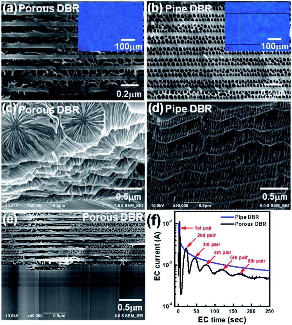 | ||
| Fig. 1 Cross-sectional SEM micrographs of (a) the Porous-DBR structure and (b) the Pipe-DBR structure with the insets showing the OM images. Tilted-views of the sample peeling regions of (c) the Porous-DBR structure and (d) the Pipe-DBR structure. (e) The last 4th pair of the n+-GaN:Si/u-GaN stack structure has an incompletely etched GaN:Si layer in the Porous-DBR structure. (f) Currents measured as a function of the EC etching time. | ||
After the sample cleavage process for the SEM sample preparation, the peeling off region for the Porous-DBR structure observed in Fig. 1c exhibits multiple radiative patterns due to the etchant ions reacting with the n+-GaN:Si layers through a top–down diffusion process from surfaces. On the other hand, in Fig. 1d, the peeling off region, for the Pipe-DBR structure, shows that the holes straightly extend from the laser scribing ditch, confirming the pipe-like feature in these etched GaN:Si layers. This implies that the etchants can efficiently diffuse into and react with the GaN:Si layer through the assistance of these laser scribed channels under the external positive bias voltage. In the Porous-DBR structure, this can be supported by the cross-sectional SEM micrograph shown in Fig. 1e, where the last 4th pair of the n+-GaN:Si/u-GaN stack structure has an incompletely etched GaN:Si layer. The etchants can diffuse in the top–down direction through the dislocations or defect regions to etch the bottom n+-GaN:Si layers. This is because the GaN epitaxial layer grown on the lattice-mismatched sapphire substrate has high dislocation density. The EC wet etching process is not a violent chemical reaction that the N2 product didn't explode and peel-off on the epitaxial layer. Comparing the etching currents as a function of etching time with an applied bias of +8 V in both DBR structures (Fig. 1f), oscillating currents and smooth etching currents have been observed in the Porous-DBR and the Pipe-DBR structures, respectively. The oscillation characteristic in the Porous-DBR structure confirms that the etching process is dominated by the top–down diffusion of etchants. When the etchants pass through the u-GaN layer and reach the underlying n+-GaN:Si layer, the etching current is increased in the initial stage of the radiative etching process. The current reaches the maximum and starts to decrease when half of the n+-GaN:Si layer is etched. After the etching reaction is completed on the entire layer, the minimum current is obtained. Since the diffusion process is also time dependent, a longer period is required to accomplish the etching process of adjacent stacking pairs. Interestingly, smooth and exponential decay of the current in the Pipe-DBR structure indicates that a uniform lateral etching process occurred on all n+-GaN:Si layers of the stacked structure at the same time. After the laser scribing process, all the n+-GaN:Si layers close to the LS lines were exposed in the etching solution for the EC wet etching process. By increasing the EC wet etching time, the non-etched area between two LS lines decreased and the effective resistance of the etched sample increased, which induced reduction of the measured current.
More detailed structural information of the Pipe-DBR was obtained by X-ray diffraction techniques with incident light parallel or perpendicular to the longitudinal direction of pipes as schematically shown in Fig. 2a. The non-treated LED structure with the epitaxial stack structure is defined as the standard-LED (ST-LED). The typical normal scan of the Pipe-DBR sample compared to the ST-LED is shown in Fig. 2b. Only the sets of the sapphire and GaN (0 0 0 L) peaks without other orientations are presented, implying that each constituent in the Pipe-DBR structure still maintains a high epitaxial relationship with sapphire and no secondary phases are observed after the EC wet etching process. In addition, a magnified section of the XRD curves at around the sapphire (0 0 0 10) index shown in the inset of Fig. 2b also exhibits that the GaN (0 0 0 4) peak position of the Pipe-DBR is toward a smaller reciprocal lattice index (or a smaller 2θ angle) than that of the ST-LED. The c-axis lattice constants of GaN extracted from the diffraction peak positions in the inset are 5.187 Å for the Pipe-DBR and 5.169 Å for the ST-LED, respectively. Compared to the bulk value of GaN (5.186 Å), the strain of GaN in the Pipe-DBR is nearly fully relaxed, whereas GaN in the ST-LED still suffers a very high compressive strain. Moreover, the surface normal reciprocal space maps (RSMs) along the X-ray incident direction parallel (Fig. 2c) or perpendicular (Fig. 2d) to the longitudinal axis of the pipes were also collected. In both RSMs, the diffraction spots of GaN (0 0 0 4) are located at the same position of the sapphire-based reciprocal lattice unit (L = 10.015), representing that the EC wet etching process would not result in lattice collapse or tilting in the lattice structure of GaN. However, they have completely different scattering features, where a typical round shape and a radial shape of diffraction patterns have been observed correspondingly. For the parallel case (Fig. 2c), the round shape of the diffraction pattern confirms that pipe holes uniformly and straightly pass through the whole heavily doped GaN layer without being interrupted inside. On the other hand, for the perpendicular case (Fig. 2d), the radial shape of the diffraction pattern can be attributed to the reflections of some special facets because most pipe holes are present in polygonal forms such as triangles, hexagons, and so on instead of circles, which can be identified by careful observation of the cross-section SEM images (Fig. 1b). Such a pipe-like DBR structure can therefore lead to very unique anisotropic optical behaviors that are unveiled in the following experiments.
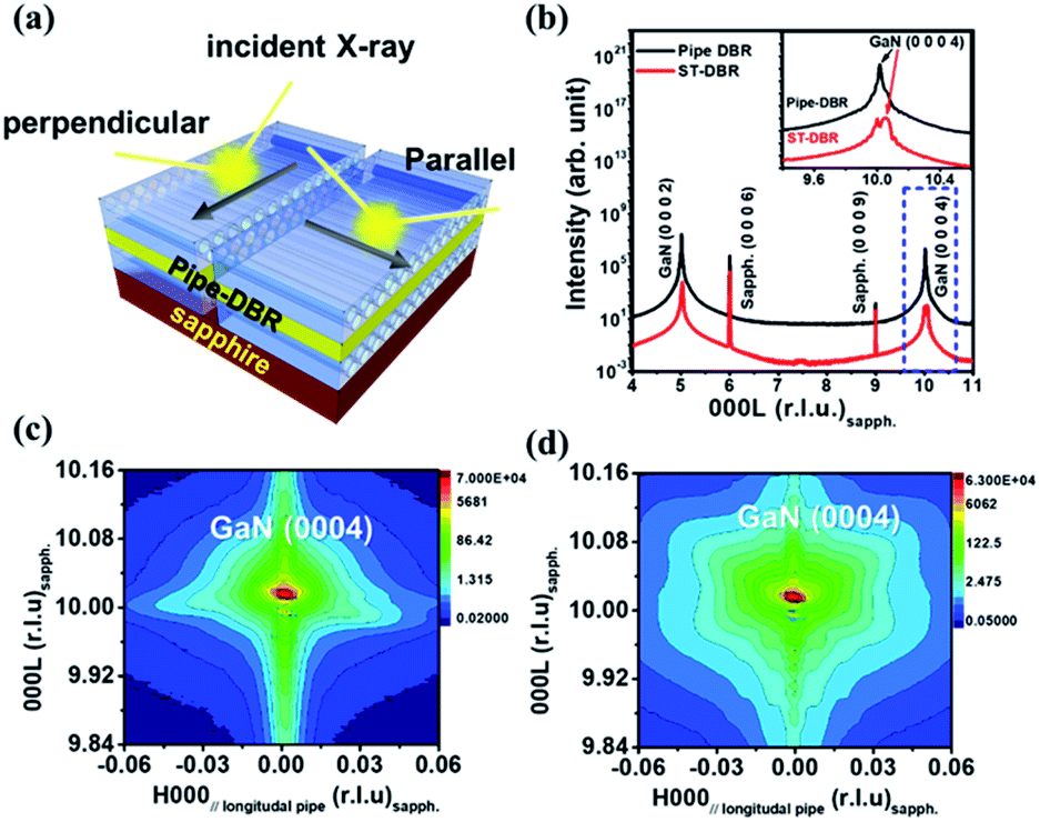 | ||
| Fig. 2 (a) Schematic of the Pipe-DBR architecture and the relative X-ray diffraction measurement methods. (b) The normal scans of the X-ray diffraction curves of the pipe GaN and ST-LED samples. The inset is the magnified region around the GaN (0 0 0 4) diffraction peaks. The RSMs of GaN (0 0 0 4) reflection were measured with the beam incident direction (c) parallel and (d) perpendicular to the longitudinal axis of the pipes, respectively. | ||
In Fig. 3, angle-dependent reflectance spectra of the Porous-DBR and the Pipe-DBR structures were measured by varying the detection angles from 20° to 60°. In Fig. 3a, the central wavelength and the reflectivity of the Porous-DBR structure were measured to be 478.1 nm/97.2% at 20° and 446.7 nm/95.5% at 60°, respectively. For the Pipe-DBR structure in Fig. 3b, the central wavelength and the reflectivity of the Pipe-DBR structure were measured to be 487.0 nm/96.6% at 20° and 455.1 nm/96.2% at the 60° detection angle. During the light reflectance measurement, the spot size of the incident light illuminating on several LS lines is about 1 mm diameter. The light scattering process occurs on the LS lines, reducing the peak reflectance slightly. By increasing the detection angle, the central wavelengths of both DBR reflectors are shifted to short wavelengths. The equation of the Bragg spectral position (λB) against the angle is expressed.39
 | (1) |
:Si/u-GaN pair, n is the average refractive index of pair layers, and θ is the incident angle with respect to the surface.
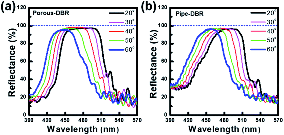 | ||
| Fig. 3 Angle-dependent reflectance spectra of (a) the Porous-DBR structure and (b) the Pipe-DBR structure at detection angles from 20° to 60°. The incident light is the non-polarized light source that is illuminated on the DBR structure for reflectance measurements. | ||
In Fig. 4, the polarization-dependent reflectance spectra were measured by varying the rotation angle of the linear polarizer from 0° (parallel to the LS line, perpendicular to the pipe-GaN direction) to 90° (perpendicular to the LS line) to control the incident linear polarized light. The reflectivity and the central wavelength of the Porous-DBR were measured to be 95.4%/478.3 nm at 0° and 97.4%/479.8 nm at 90° polarization angles as shown in Fig. 4a, which shows that the reflectance spectra are very stable and are almost independent of the rotation angles of the linear polarizer.
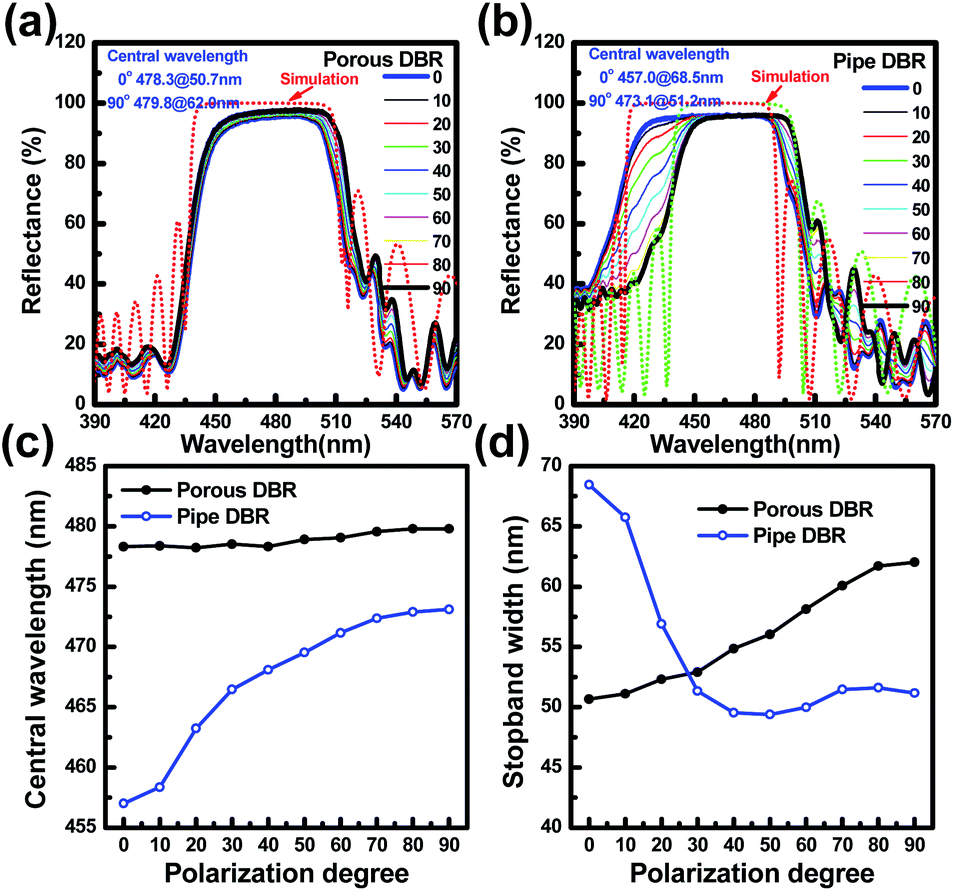 | ||
| Fig. 4 Polarization-dependent reflectance spectra of (a) the Porous-DBR structure and (b) the Pipe-DBR structure. The simulation reflectance spectra are shown. (c) The central wavelength and (d) the stopband width as a function of the polarization degree. | ||
However, in Fig. 4b, the reflectivity and the central wavelength of the Pipe-DBR were measured to be 95.8%/457.0 nm at 0° and 96.0%/473.1 nm at 90°. The central wavelength of the high reflectance spectra has an obvious shift of 16.1 nm toward longer wavelengths by varying the rotation angle of the polarizer from 0° to 90°. The simulation reflectance spectra of both DBR structures are shown in Fig. 4a and b. The reflectance spectrum of the Pipe-DBR has polarization-dependent properties that the central reflectance wavelength at 0° polarization degree was located at a short wavelength. In the Pipe-DBR structure, the superposition of the polarized reflectance spectra has a slightly high reflectivity at 400 nm. The central wavelength of the Porous-DBR is almost the same at around 478 nm under different rotation angles of the linear polarizer, whereas that of the Pipe-DBR structure shows a strong dependence on the polarizer angle (Fig. 4c). According to the stopband width of the DBR structure, defined as the wavelength region, the reflectivity is higher than 90% in the reflectance spectrum. Moreover, the central wavelength and the stopband width of the Pipe-DBR structure in Fig. 4d have a larger variation from 457.0 nm/68.5 nm at 0° to 473.1 nm/51.2 nm at 90°, which is caused by the anisotropic refractive index on the directional pipe GaN layer in the stacked DBR structure. In the Pipe-DBR structure, the large refractive index difference at 0° polarization degree induced the wide stopband width and short central wavelength of the DBR spectrum compared with that at 90° polarization degree. The stopband width of the Pipe-DBR structure decreased which was caused by the decrease of the refractive index difference by increasing the polarization degree.
By varying the polarization degree, the effective refractive index of porous layers in both DBR structures was derived from the optical response as shown in Fig. 5. From the central wavelength of the reflectance spectra, the effective refractive index can be calculated as 1.95 along the pipe-GaN layer (n‖) at 90° polarization degree, 1.83 perpendicular to the pipe-GaN layer (n⊥) at 0° polarization degree, and 1.99 for the random porous GaN layer where the refractive index of the un-etched u-GaN layer is about 2.45.40 The refractive index difference of the pipe GaN layer (Δn = n‖ − n⊥) is about 0.12 (4.9%) compared with the u-GaN layer. By rotating the linear polarizer, the effective refractive index of the pipe-GaN layer should be changed between 1.95 (n‖) and 1.83 (n⊥) depending on the angle between the directions of the pipe and the linear polarizer.
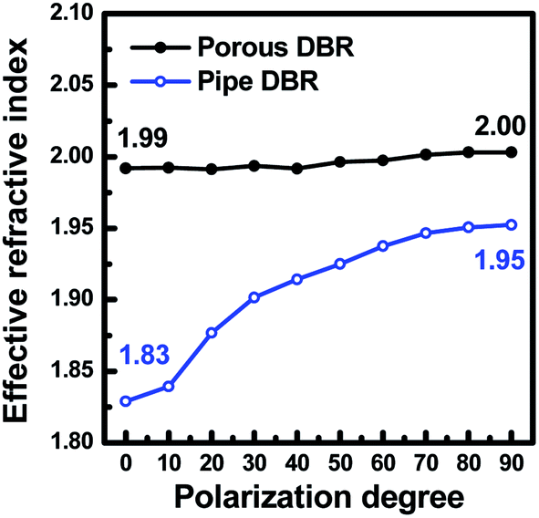 | ||
| Fig. 5 By varying the polarization degree, the effective refractive index of porous layers in both DBR structures was derived from the optical response. | ||
The typical load-penetration depth curves of the nanoindentation test41,42 for the InGaN LED with and without the EC-treated DBR structures are presented in Fig. 6a. The deformation of the GaN-based epitaxial structures included a purely elastic response and elastoplastic behavior during loading, and an elastic behavior was observed during unloading.
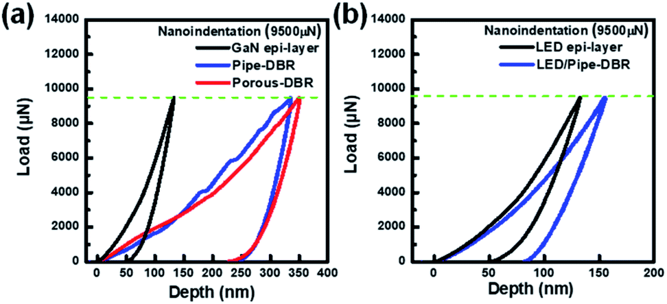 | ||
| Fig. 6 The typical load-penetration depth curves of (a) EC-treated DBR structures and (b) the InGaN LED with EC-treated DBR structures. | ||
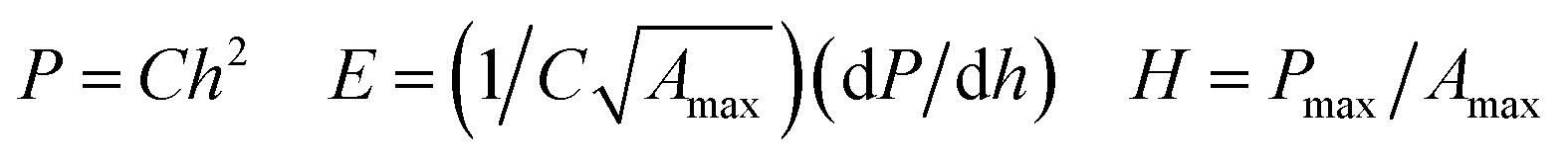
The elastic modulus and hardness values were extracted from the load-penetration depth curves through the software in the nanoindentation measurement. A UMIS nanoindenter with a Berkovich diamond indenter (tip radius 100 nm, edge angle 130.6°) was used to measure the mechanical properties (elastic modulus and hardness). A load cell and a displacement voltage dilatometer were used to control the applied load, P, and to measure the penetration depth of the indenter, h. From the load-depth curves and the following equations,43 the elastic modulus, E, and hardness, H, were extracted:
 | (2) |
The power-dependent PL spectra were measured by using a 266 nm laser as an exciting source with a 100 μm-diameter laser spot size. By varying the laser-excited power through the neutral density filters in Fig. 7a, the PL spectra of the non-treated n+-GaN/u-GaN stack structure exhibit two typical peaks at wavelengths of 359.7 nm for the u-GaN layer and 368.1 nm for the n+-GaN:Si layer, respectively. However, in the Pipe-DBR with the directional pipe GaN structure, the spectra show unusual lasing-like peaks located at 359.7 nm as shown in Fig. 7b. In Fig. 7c, the full width at half maximum (FWHM) and the emission intensities of the PL spectra were measured in the Pipe-DBR structure. A very sharp width of 1.36 nm can be even observed at a high laser pumping power density (1.17 mW, 14.9 W cm−2) as shown in Fig. 7c. A non-linear PL intensity was observed by increasing the laser pumping power. In Fig. 7b, a stimulated emission peak was observed in the porous-GaN:Si layer which was caused by the quantum confinement effect on the nano-structure of the residual n+-GaN:Si layers. The optically pumped lasing phenomenon observed on the pipe-GaN structure indicates the high crystalline quality of the residual n+-GaN:Si layers.
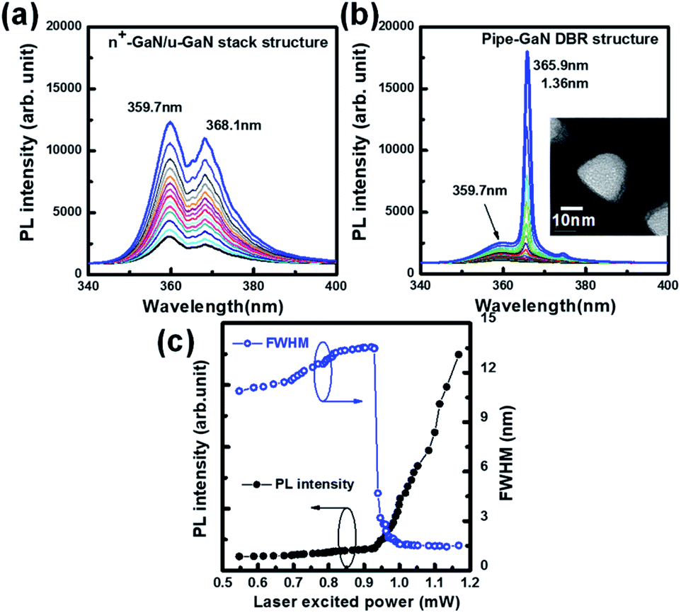 | ||
| Fig. 7 The PL spectra of the (a) non-treated n+-GaN/u-GaN stack structure and (b) EC-etched pipe-GaN DBR structure measured by varying the laser power of the 266 nm laser. The TEM micrograph of the air-void structure is shown in the inset. (c) The PL intensity and the line-width of the PL spectra. | ||
The crystalline properties of the unetched GaN, close to the air-void structure, show a single crystal structure in the transmission electron microscope (TEM) micrograph inserted in Fig. 7b. The n+-GaN:Si layers in the stack structure have been etched as a nano-size GaN:Si sidewall structure nearby the air-void structure. Besides, the peak wavelengths of the PL spectra shifted from 368.1 nm for the bulk n+-GaN:Si layer to 365.9 nm for the pipe-GaN:Si nanostructure which can be attributed to the quantum confinement effect on the residual nano-size n+-GaN:Si sidewall in the Pipe-DBR structure.
To analyze the directional pipe-GaN structure, the cross-channel patterns on the n+-GaN/u-GaN stack structure were prepared through the laser scribing process with 230 μm-spacing between two LS lines. The lateral wet etching direction is perpendicular to each LS line with an external bias voltage. After the EC etching process, the OM images of the pipe-GaN DBR with the incident polarized light controlled by rotating the linear polarizer are unveiled as shown in Fig. 8. Two directional lateral wet etching fronts, from the x-axis (90°) and y-axis (0°) LS lines, are merged into the diagonal directions that the arrow patterns can be observed clearly in the polarized optical images. At 0° degree of the linear polarizer, the OM images of the Pipe-GaN DBR reveal clear arrow patterns in the diagonal directions as shown in Fig. 8a and b. When the rotation angle of the linear polarizer is −45° as shown in Fig. 7c, brighter contrast emerging in −45° arrow patterns indicates that it has higher reflective light compared to 45° arrow patterns. When the linear polarizer rotates to −90° as shown in Fig. 7d, the intensity of the pattern region is higher than that at 0° in Fig. 8b. A high light contract region surrounding the arrow patterns in the diagonal directions is observed, where the directions of linear polarizers are perpendicular to each other. The anisotropic light refractive index of the pipe-GaN structure has been observed along and perpendicular to the pipe GaN structure as shown in Fig. 4b. The effective light refractive index difference of the pipe-GaN layer is caused by the porosity difference along and perpendicular to the pipe GaN structure. Symmetric and repeated arrow patterns are observed clearly in the polarized OM images which indicated that the directional lateral wet etching paths can be well controlled through the EC etching process. The central wavelength of the Pipe-DBR structure has a strong dependence on the direction of the EC-etched pipe structure as shown in Fig. 4b.
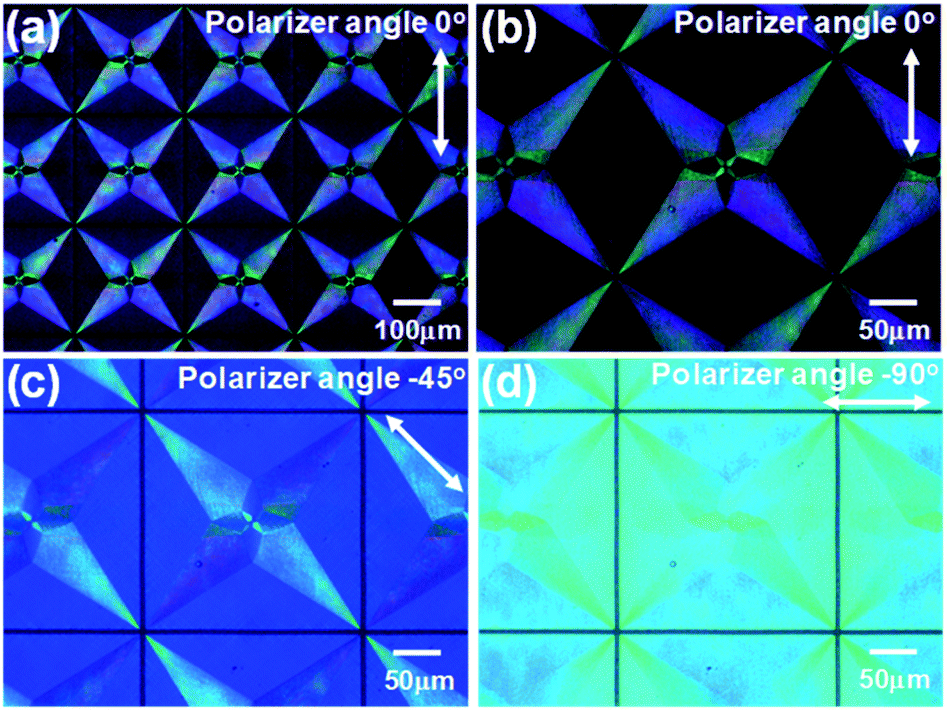 | ||
| Fig. 8 (a) Polarized OM images is observed with a 10× objective lens at the 45° cross-angle between the polarizer/analyzer. Polarized OM image with a 20× objective lens at the (b) 0° cross-angle, (c) 45° cross-angle, and (d) 90° cross-angle between the polarizer/analyzer. | ||
The color difference of the OM image is caused by the central wavelength shift of the Pipe-DBR structure that depended on the angle between the directions of the pipe and linear polarizer. The color change of the arrow pattern is caused by the anisotropic refractive index in the Pipe-DBR structure in different pipe directions.
Conclusions
A high reflectance Pipe-DBR structure has been fabricated by a simple EC wet etching process. The polarization-dependent reflectance spectra of the Pipe-DBR structure reveal that the pipe-GaN layers have the anisotropic refractive index. The InGaN LED structure with the embedded Pipe-GaN structure still maintains suitable mechanical properties compared to the non-treated LED structure. Lasing-like emission properties can be observed in the pipe GaN structure, confirming the high crystalline quality and the quantum-confinement effect on the residual pipe-GaN structure. Arrow patterns can be observed clearly in the polarized OM images, indicating that the directional lateral wet etching paths can be well controlled. The Pipe-DBR structure has a high reflectance and polarization-dependent central wavelength. This study provide a way to develop potential polarized light sources and VCSEL devices.Conflicts of interest
There are no conflicts to declare.Acknowledgements
The authors gratefully acknowledge the financial support for this research by the Ministry of Science and Technology of Taiwan under grant no. 107-2221-E-005-061, 108-2221-E-005-064, and MOST 107-2112-M-005-006. It was further supported by the Innovation and Development Center of Sustainable Agriculture's Featured Areas Research Center Program within the framework of Taiwan's Ministry of Education’s Higher Education Sprout Project. The authors also thank Prof. Shou-Yi Chang with National Tsing Hua University for his contributions.References
- S. Nakamura, Science, 1998, 281, 956–962 CrossRef CAS PubMed.
- T. Someya, R. Werner, A. Forchel, M. Catalano, R. Cingolani and Y. Arakawa, Science, 1999, 285, 1905–1906 CrossRef CAS PubMed.
- R. Butté, E. Feltin, J. Dorsaz, G. Christmann, J. F. Carlin, N. Grandjean and M. Ilegems, Jpn. J. Appl. Phys., Part 1, 2005, 44, 7207–7216 CrossRef.
- N. Nakada, M. Nakaji, H. Ishikawa, T. Egawa, M. Umeno and T. Jimbo, Appl. Phys. Lett., 2000, 76, 1804–1806 CrossRef CAS.
- K. E. Waldrip, J. Han, J. J. Figiel, H. Zhou, E. Makarona and A. V. Nurmikko, Appl. Phys. Lett., 2001, 78, 3205–3207 CrossRef CAS.
- P. S. Yeh, M. C. Yu, J. H. Lin, C. C. Huang, Y. C. Liao, D. W. Lin, J. R. Fan and H. C. Kuo, IEEE Photonics Technol. Lett., 2014, 26, 2488–2491 Search PubMed.
- C. F. Lin, H. H. Yao, J. W. Lu, Y. L. Hsieh, H. C. Kuo and S. C. Wang, J. Cryst. Growth, 2004, 261, 359–363 CrossRef CAS.
- J. Dorsaz, J. F. Carlin, S. Gradecak and M. Ilegems, J. Appl. Phys., 2005, 97, 084505 CrossRef.
- J. F. Carlin and M. Ilegems, Appl. Phys. Lett., 2003, 83, 668–670 CrossRef CAS.
- C. Berger, A. Dadgar, J. Bläsing and A. Krost, J. Cryst. Growth, 2013, 370, 87–91 CrossRef CAS.
- M. Kuramoto, S. Kobayashi, T. Akagi, K. Tazawa, K. Tanaka, T. Saito and T. Takeuchi, Appl. Phys. Express, 2018, 11, 112101 CrossRef.
- R. Sharma, E. D. Haberer, C. Meier, E. L. Hu and S. Nakamura, Appl. Phys. Lett., 2005, 87, 051107 CrossRef.
- J. Park, J. H. Kang and S. W. Ryu, Appl. Phys. Express, 2013, 6, 072201 CrossRef.
- D. Chen and J. Han, Appl. Phys. Lett., 2012, 101, 221104 CrossRef.
- T. Mitsunari, T. Tanikawa, Y. Honda, M. Yamaguchi and H. Amano, J. Cryst. Growth, 2013, 370, 16–21 CrossRef CAS.
- R. Tao, M. Arita, S. Kako, K. Kamide and Y. Arakawa, Appl. Phys. Lett., 2015, 107, 101102 CrossRef.
- A. Szyszka, L. Lupina, G. Lupina, M. Mazur, M. A. Schubert, P. Storck, S. B. Thapa and T. Schroeder, Appl. Phys. Lett., 2014, 104, 011106 CrossRef.
- T. Grinys, R. Dargis, A. Kalpakovaite, S. Stanionyte, A. Clark, F. E. Arkun, I. Reklaitis and R. Tomašiunas, J. Cryst. Growth, 2015, 424, 28–32 CrossRef CAS.
- Y. Yang, Y. Lin, P. Xiang, M. Liu, W. Chen, X. Han, G. Hu, G. Hu, W. Zang, X. Lin, Z. Wu, Y. Liu and B. Zhang, Appl. Phys. Express, 2014, 7, 042102 CrossRef.
- B. Damilano, S. Brochen, J. Brault, T. Hossain, F. Réveret, E. Frayssinet, S. Chenot, A. Courville, Y. Cordier and F. Semond, Phys. Status Solidi A, 2015, 212, 2297–2301 CrossRef CAS.
- B. S. Cheng, C. H. Chiu, M. H. Lo, Y. L. Wu, H. C. Kuo, T. C. Lu, Y. J. Cheng, S. C. Wang and K. J. Huang, IEEE Photonics Technol. Lett., 2011, 23, 642–644 CAS.
- W. Y. Lin, D. S. Wuu, S. C. Huang and R. H. Horng, IEEE Trans. Electron Devices, 2011, 58, 173–179 CAS.
- T. Jeong, H. H. Lee, S. H. Park, J. H. Baek and J. K. Lee, Jpn. J. Appl. Phys., 2008, 47, 8811–8814 CrossRef CAS.
- S. Y. Kuo, K. BinHong and T. C. Lu, IEEE J. Quantum Electron., 2015, 51, 3300805 Search PubMed.
- L. Zhang, S. Wang, Y. Shao, Y. Wu, C. Sun, Q. Huo, B. Zhang, H. Hu and X. Hao, Sci. Rep., 2017, 7, 44063 CrossRef PubMed.
- T. H. Ngo, B. Gil, T. V. Shubina, B. Damilano, S. Vezian, P. Valvin and J. Massies, Sci. Rep., 2018, 8, 15767 CrossRef PubMed.
- C. Yang, L. Liu, S. Zhu, Z. Yu, X. Xi, S. Wu, H. Cao, J. Li and L. Zhao, J. Phys. Chem. C, 2017, 121, 7331–7336 CrossRef CAS.
- X. Lu, J. Li, K. Su, C. Ge, Z. Li, T. Zhan, G. Wang and J. Li, Nanomaterials, 2019, 9, 862 CrossRef CAS PubMed.
- B. C. Shieh, Y. C. Jhang, K. P. Huang, W. C. Huang, J. J. Dai, C. F. Lai and C. F. Lin, Appl. Phys. Express, 2015, 8, 082101 CrossRef.
- C. Zhang, S. H. Park, D. Chen, D. W. Lin, W. Xiong, H. C. Kuo, C. F. Lin, H. Cao and J. Han, ACS Photonics, 2015, 2, 980–986 CrossRef CAS.
- S. Mishkat-Ul-Masabih, T. S. Luk, A. Rishinaramangalam, M. Monavarian, M. Nami and D. Feezell, Appl. Phys. Lett., 2018, 112, 041109 CrossRef.
- C. Berger, A. Lesnik, T. Zettler, G. Schmidt, P. Veit, A. Dadgar, J. Bläsing, J. Christen and A. Strittmatter, J. Cryst. Growth, 2016, 440, 6–12 CrossRef CAS.
- S. Chen, C. Zhang, J. Lee, J. Han and A. Nurmikko, Adv. Mater., 2017, 29, 1604781 CrossRef PubMed.
- H. P. Springbett, K. Gao, J. Jarman, T. Zhu, M. Holmes, Y. Arakawa and R. A. Oliver, Appl. Phys. Lett., 2018, 113, 101107 CrossRef.
- M. J. Miah, A. Al-Samaneh, A. Kern, D. Wahl, P. Debernardi and R. Michalzik, IEEE J. Sel. Top. Quantum Electron., 2013, 19, 1701410 Search PubMed.
- R. Tao, M. Arita, S. Kako and Y. Arakawa, Appl. Phys. Lett., 2013, 103, 201118 CrossRef.
- S. M. Mishkat-Ul-Masabih, T. S. Luk, M. Monavarian and D. F. Feezell, Opt. Express, 2019, 27, 9495 CrossRef CAS PubMed.
- C. F. Lin, J. J. Dai, M. S. Lin, K. T. Chen, W. C. Huang, C. M. Lin, R. H. Jiang and Y. C. Huang, Appl. Phys. Express, 2010, 3, 031001 CrossRef.
- C. López-López, S. Colodrero, M. E. Calvo and H. Míguez, Energy Environ. Sci., 2013, 6, 1260 RSC.
- W. J. Hsu, K. T. Chen, W. C. Huang, C. J. Wu, J. J. Dai, S. H. Chen and C. F. Lin, Opt. Express, 2016, 24, 11601 CrossRef CAS PubMed.
- M. S. Lin, C. F. Lin, W. C. Huang, G. M. Wang, B. C. Shieh, J. J. Dai, S. Y. Chang, D. S. Wuu, P. L. Liu and R. H. Horng, Appl. Phys. Express, 2011, 4, 062101 CrossRef.
- R. Nowak, M. Pessa, M. Suganuma, M. Leszczynski, I. Grzegory, S. Porowski and F. Yoshida, Appl. Phys. Lett., 1999, 75, 2070–2072 CrossRef CAS.
- S. Y. Chang and T. K. Chang, J. Appl. Phys., 2007, 101, 033507 CrossRef.
- G. Y. Shiu, K. T. Chen, F. H. Fan, K. P. Huang, W. J. Hsu, J. J. Dai, C. F. Lai and C. F. Lin, Sci. Rep., 2016, 6, 1–8 CrossRef PubMed.
| This journal is © The Royal Society of Chemistry 2020 |