
 Open Access Article
 This Open Access Article is licensed under a Creative Commons Attribution-Non Commercial 3.0 Unported Licence
Enhanced strength of nano-polycrystalline diamond by introducing boron carbide interlayers at the grain boundaries†
Bo
Zhao
 a,
Shengya
Zhang
a,
Shuai
Duan
a,
Jingyan
Song
a,
Xiangjun
Li
a,
Bingchao
Yang
*a,
Xin
Chen
a,
Chao
Wang
a,
Wencai
Yi
a,
Zhixiu
Wang
b and
Xiaobing
Liu
*a
a,
Shengya
Zhang
a,
Shuai
Duan
a,
Jingyan
Song
a,
Xiangjun
Li
a,
Bingchao
Yang
*a,
Xin
Chen
a,
Chao
Wang
a,
Wencai
Yi
a,
Zhixiu
Wang
b and
Xiaobing
Liu
*a
aLaboratory of High Pressure Physics and Material Science, School of Physics and Physical Engineering, Qufu Normal University, Qufu, Shandong Province 273165, China. E-mail: xiaobing.phy@qfnu.edu.cn; yangbc@qfnu.edu.cn
bAdministrative Office of Laboratory and Equipment, Qufu Normal University, Qufu, Shandong Province 273165, China
First published on 9th December 2019
Abstract
Polycrystalline diamond with high mechanical properties and excellent thermal stability plays an important role in industry and materials science. However, the increased inherent brittle strength with the increase of hardness has severely limited its further widespread application. In this work, we produced well-sintered nano-polycrystalline (np) diamond by directly sintering fine diamond powders with the boron carbide (B4C) additive at high pressure and high temperatures. The highest hardness value of up to ∼90 GPa was observed in the np-diamond (consisting of fine grains with a size of 16 nm) by adding 5 wt% B4C at 18 GPa and 2237 K. Moreover, our results reveal that the produced samples have shown noticeably enhanced strength and toughness (18.37 MPa m0.5) with the assistance of the soft phase at the grain boundaries, higher than that of the hardest known nano-twined diamond by ∼24% and a little greater than that of the toughest CVD diamond (18 MPa m0.5). This study offers a novel functional approach in improving and controlling the hardness and stiffness of polycrystalline diamond.
1. Introduction
Diamond, the hardest known material, has been attracting continuous interest for decades in cutting tools and applications in high-pressure science because of its excellent mechanical properties, high thermal conductivity and chemical stability.1–8 However, the great challenge to shape, limited physical dimensions and high cost of nearly perfect single-crystal (sc) diamonds have severely limited their widespread technological application in some extreme environments. In addition, previous studies have found that the inherent brittle strength would increase obviously with the increase of hardness of diamond.9–11 In the cases of sc-diamond cutting tools and high-pressure anvils, the practical operating limits are usually set by catastrophic cleavage fracture. Therefore, enhancing the strength of diamond and diamond-like superhard materials is always one of the most important topics in the materials science community.12–15Polycrystalline structures often show superior mechanical properties over corresponding monocrystals.16–20 In recent years, a series of nano-polycrystalline (np) and nano-twinned (nt) materials have been successfully synthesized through direct conversions of certain precursors (e.g. carbon nanotubes, C60, glassy carbon, onion-like boron nitride and graphite) at extreme high pressure and high temperatures (HPHT).21–25 A breakthrough was achieved by Tian's group in the fabrication of nt-diamond which is about two-fold harder than natural diamond, together with higher fracture toughness (15 MPa m0.5) and in-air oxidation temperature.3 Extensive experimental and theoretical studies had been devoted to further strengthening polycrystalline superhard materials, involving controlled creation of composted phases, internal defects, stacking faults and interface boundaries.13,14,26–29
Diamond particles can be sintered into strong masses in crystalline forms directly by HPHT methods, consisting of easily controllable physical dimensions, shape and fine grain size.1,10 The introduction of other superhard materials (cBN) in the np-diamond was found to effectively improve its mechanical and stability properties.30–32 Low-cost boron carbide (B4C), in comparison to other high-performance ceramics, has low density, high fracture toughness, high Hugoniot elastic limit and good electrical conductivity.33,34 Reddy et al.33 revealed that the nanopores and weak interface phase in np-B4C were effective in enhancing the fracture toughness, plasticity and compression strength of the sintered brittle ceramic simultaneously. Thus we expect that sintered np-diamond would have interesting properties with the aid of the properties of B4C.
In this work, we show that we have successfully produced well-sintered np-diamond by directly sintering nano diamond powders with the B4C additive. The mechanical properties of the produced samples have been investigated by micro-indentation testing with diamond Vickers indenters. These sintered np-diamonds show high hardness, enhanced fracture toughness and thermal stability. Microstructural observations by transmission electron microscopy (TEM) and chemical bonding analysis by X-ray photoelectron spectroscopy (XPS) suggest that the existence of B4C interfaces at diamond grain boundaries and the bonding strength play key roles in controlling the hardness and stiffness of the fabricated np-diamond. This work provides a new functional approach in improving and controlling the hardness and stiffness of polycrystalline diamond.
2. Experimental section
2.1 Sample preparation
We use high-quality nano-diamond powders (∼10–30 nm, 99% in purity) (Fig. S1†) and commercial B4C (∼20–50 nm, 99.9% in purity) as starting materials. The mixed starting materials with 3 wt% and 5 wt% B4C were mechanically ground for 2 hours under ambient conditions. Then, the pre-synthesis was conducted at 6.5 GPa and temperature of 1750–1950 K employing a China type large-volume press (SPD-6 × 1200) with a holding time of 2 hours. Experiment temperatures were detected using a Pt-30% Rh/Pt-6% Rh thermocouple junction equipped within 0.5 mm of the precursors. Pressure was calibrated repeatedly by the conversion process of graphite to diamond. The recovered samples were black and opaque, ∼8 mm in diameter and 5 mm in height. The produced cylinders were cut into 2 mm in diameter and treated at 18 GPa and 2273 K for 2 hours using a 1000-ton multi-anvil producing colorless run products (Fig. S2†) at GSECARS (Sector 13) of Advanced Photon Source, Argonne National Laboratory. This process is schematically shown in Fig. 1.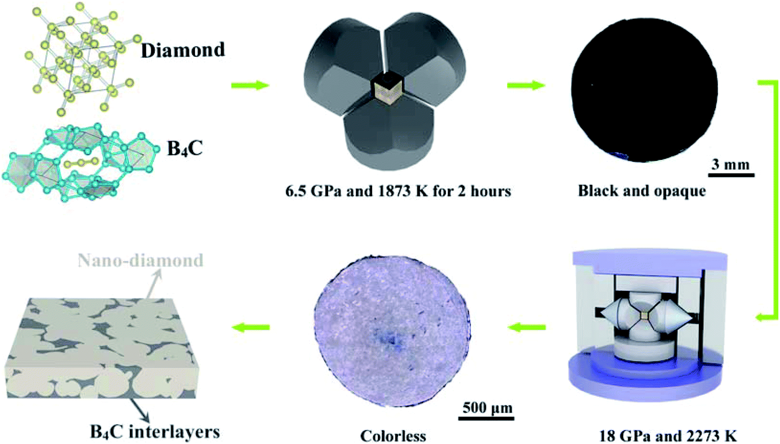 | ||
| Fig. 1 Schematic of the experimental approach showing the fabrication of sintered polycrystalline diamond by the HPHT method. | ||
2.2 Characterization
Scanning electron microscopy (SEM) and energy-dispersive X-ray spectroscopy (EDS) measurements were carried out using a Zeiss Sigma 500 microscope. Raman spectroscopy was performed using a Horiba LabRAM HR Evolution with excitation at 532 nm. XPS data were obtained using a Thermo ESCALAB 250XI. A powder X-ray diffraction (XRD) diffractometer (Ultima IV 185) was employed to study the structure of the produced samples. XPS data were analyzed with the Fityk software. High-resolution TEM (HRTEM), selected-area electron diffraction (SAED) and elemental mapping were carried out on a JEM-2100PLUS80-200 kV.2.3 Hardness and fracture toughness testing
Vickers hardness tests were carried out with a normal pyramid diamond indenter (KB5). Reliable hardness values were indicated by the asymptote which was obtained through changing the loading forces constantly in the range from 0.98 to 9.8 N, and the forces were applied with a steady loading rate; the implemented standard time of loading and dwelling was 6 s and 14 s respectively. HV was calculated through the equation HV = 2F![[thin space (1/6-em)]](https://www.rsc.org/images/entities/char_2009.gif) sin136°/L2, where F (in newton) is the loading force and L (in micrometer) is the mean value of the two diagonals.31 The accurate diagonal length of each indentation was measured using a microscope with a hardness detector. The equation
sin136°/L2, where F (in newton) is the loading force and L (in micrometer) is the mean value of the two diagonals.31 The accurate diagonal length of each indentation was measured using a microscope with a hardness detector. The equation 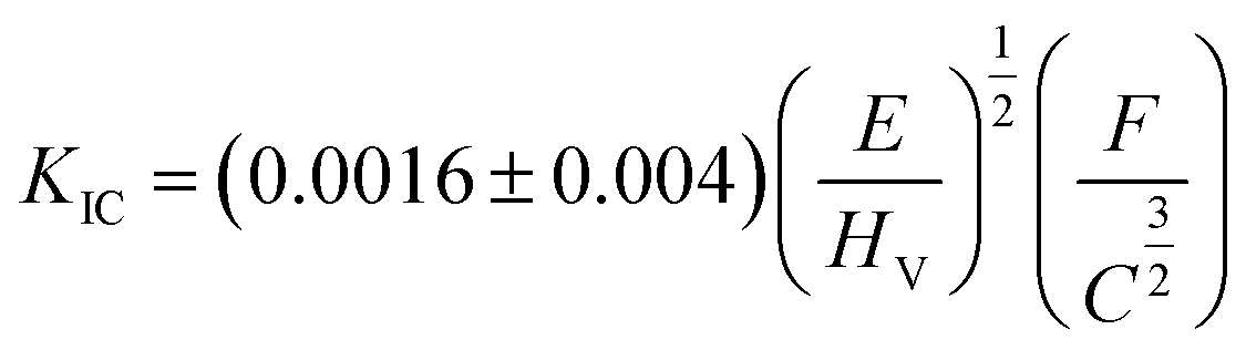 was used to calculate the fracture toughness, where HV is the hardness corresponding to the loading force, and C= (C1 + C2)/4 where C1 and C2 (in micrometer) are the diametric length of cracks.3,6 The indentations were created on the face of the polished samples and the cracks came into being from the corners of impressions meanwhile. Cracks emanating from the indentations were clearly observed using an optical microscope and their lengths can be measured accurately.
2.4 Thermal stability test
The thermal stability of the produced samples was determined by TG/DSC measurements in air in the temperature range of 303 K to 1673 K using a TG-DSC simultaneous thermal analyzer (Netzsch STA 449C). We divided the range into two sections and adopted heating rates of 20 K min−1 for the range of 303–473 K and 10 K min−1 for 473–1673 K.3. Results and discussion
High-quality polycrystalline diamond with a diameter of 1.8 mm and 3 mm in height was successfully produced at 18 GPa and 2273 K. The holding time at P/T is about 2 hours for each run. The details are summarized in Table 1.| Runs | Composition of the starting materials | D (mm) | Color | P (GPa) | T (K) | t (hours) |
|---|---|---|---|---|---|---|
| 160823-3 | np-diamonds + 3 wt% B4C | 8 | Black | 6.5 | 1750 | 2 |
| 160621-5 | np-diamonds + 5 wt% B4C | 8 | Black | 6.5 | 1950 | 2 |
| 160824-6 | np-diamonds + 3 wt% B4C | 8 | Black | 6.5 | 1750 | 2 |
| 160825-8 | np-diamonds + 3 wt% B4C | 8 | Black | 6.5 | 1800 | 2 |
| 181010-16 | np-diamonds + 3 wt% B4C | 1.8 | Light grey | 18 | 2273 | 2 |
| 181010-18 | np-diamonds + 5 wt% B4C | 1.8 | Light grey | 18 | 2273 | 2 |
The micro-Raman analysis was performed to structurally characterize the diamond/B4C composited structure. Fig. 2a shows the typical Raman spectra of nano-diamond powders and recovered samples with 5 wt% from 6.5 GPa and 1600 K, and 18 GPa and 2273 K, respectively. Compared with the nano-diamond in the starting materials (bottom curve), the Raman spectra of sintered diamond at 6.5 GPa (middle curve) show that the main peak of diamond becomes broad and shifts from 1320 to 1346 cm−1. Moreover, it is obvious that the weak peak at 1582 cm−1, associated with sp2 bonds in graphite, is significantly increased by ∼7 times, indicating the appearance of the graphitic phase under relatively low P/T conditions. The shift of the Raman bond from the pure diamond at 1332 cm−1 has been used to determine the residual stress in the sintered diamond. We can clearly see that the Raman spectrum of the sample treated at 18 GPa and 2273 K (top curve) shows a sharp peak at 1335 cm−1 and the peak at 1582 cm−1 has disappeared, indicating the high-quality crystalline structure. The peaks located in the range of low wavenumbers ∼400–1200 cm−1 for B4C could also be observed for the sintered samples.33,34 The main peaks located at 576 and 1081 cm−1 are assigned to crystalline B4C after being treated at 6.5 GPa, while these peaks of the recovered samples from the 18 GPa become weak and the peaks at 429 and 967 cm−1, by contrast, are more prominent. The XRD pattern in Fig. 2b shows no new detectable phase but amorphous carbon or graphite in the recovered samples from 18 GPa can be seen (top curve). Thus both characteristic Raman bonds and XRD results have confirmed that the sintered sample is a highly crystalline composite of diamond and B4C.
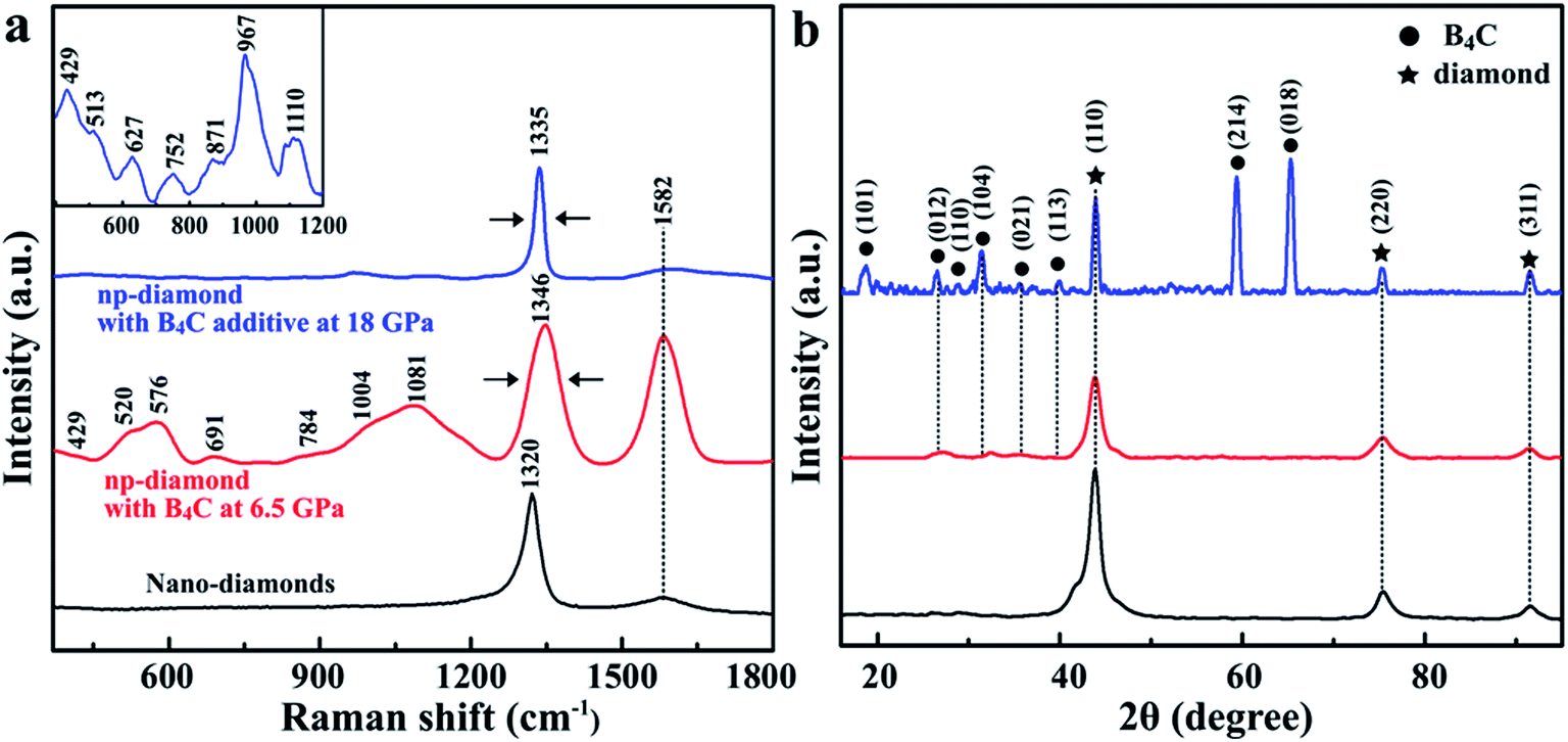 | ||
| Fig. 2 (a) Raman and (b) XRD spectra for the starting materials of nano-diamond powders (bottom curve), with the 3 wt% B4C additive treated at 6.5 GPa and 1950 K (middle curve), and the 5 wt% B4C additive at 18 GPa and 2273 K (top curve), respectively. | ||
Representative SEM images of the macrofeature of sintered polycrystalline diamond are shown in Fig. 3. Meanwhile, SEM photos of sintered diamonds and low-pressure samples are shown in Fig. S3.† In comparison, the produced high-quality sample (181010-16) with the 3 wt% B4C additive has a fine mixed texture of a homogeneous structure with randomly oriented grains in the range of ∼2 to 8 μm, as indicated in Fig. 3a. It is clear that the grains are very tightly sintered together and no obvious cracks or defects could be found in the grain boundary. Fig. 3b shows the surface morphology of produced polycrystalline diamond (181010-18) with the 5 wt% B4C additive. The aggregated diamond sample possesses a lamellar structure and high density (Fig. S4†). This structure is similar to that of the previously produced ultrahard np-diamond by direct transition from graphite under HPHT conditions. Fig. 3d and e show the EDS map of the B element (purple color) and C element (blue color) in one selected grain (Fig. 3c) of the sample (181010-18) with 5 wt% B4C. The EDS map of samples at low pressure (Fig. S5†) shows the sample distribution trend. Elemental mapping proves that the B4C is uniformly distributed over the entire area of the grain.
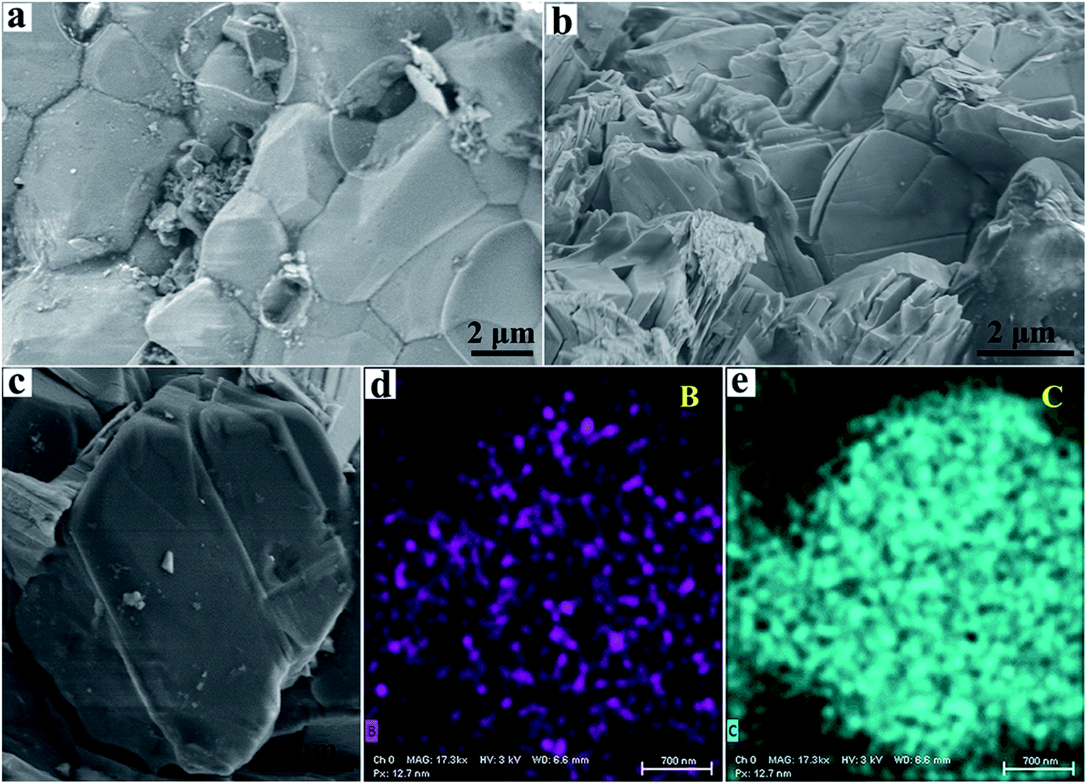 | ||
| Fig. 3 SEM images of the sintered polycrystalline diamond surfaces with 3 wt% (a) and 5 wt% (b) B4C additive. (d) and (e) the elemental mapping images of B and C in one selected grain (c), respectively. | ||
In order to determine the underlying microstructure of the produced polycrystalline diamond, we prepared a cross-sectional TEM specimen for the sample (181010-18) with 5 wt% B4C using a focused ion beam (FIB) milling technique. Characteristic TEM images are shown in Fig. 4. TEM images in Fig. 4b and c confirm that the produced polycrystalline diamond is uniform and well sintered at 18 GPa and 2273 K. The sample is composed of some aggregated grains of nano size. Moreover, unlike previously sintered polycrystalline diamond with a transition metal catalyst, it is interesting to note that there is no porosity at the interface and the grain boundaries. Fig. 4d shows a size distribution derived from 211 nanograins on the basis of HRTEM measurements. The average size of the diamond grains is ∼16 nm, which is close to the critical value (typically ∼10–15 nm) for the hardening mechanism of nano-polycrystalline materials by the Hall–Petch effect and quantum confinement effect (Fig. S6†).1,3,19,35 Such characteristics in the sintered np-diamond usually indicate strong mechanical properties.
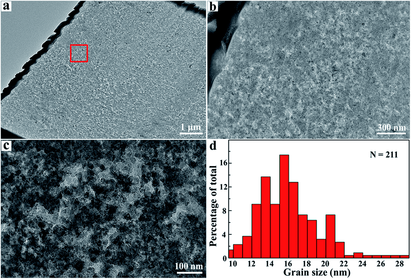 | ||
| Fig. 4 (a) Cross-sectional TEM sample prepared by FIB milling. (b and c) TEM images of the sample of the area marked with a red box in (a). (d) Grain size distribution of the produced polycrystalline diamond sample measured from the TEM image. | ||
Fig. 5 shows the typical HRTEM images and the selected area diffraction (SAED) patterns of the grain boundaries of the produced np-diamond. Fig. 5a represents the structure of the sintered diamond and no visible defects were found among the diamond grains. Three diffraction rings in SAED patterns (top inset) corresponding to the (111), (220), (311) planes of the diamond were observed which accounted for its polycrystalline structure. Fig. 5b–d display the typical interface and grain boundaries of diamond/diamond, B4C/B4C and diamond/B4C grains, respectively. Our observation shows that the two randomly distributed domains have already been stitched tightly together by HPHT treatment. The stacking faults and partial dislocations at the interfaces, as indicated by blue arrows, play an important role in releasing residual stresses within the sintered bulk materials, leading to high stability.
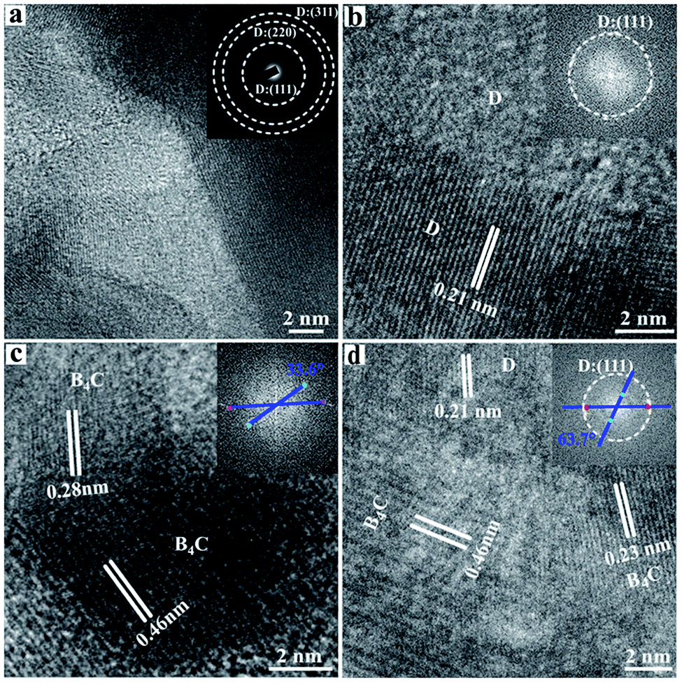 | ||
| Fig. 5 (a) Microstructure of the grain boundaries in the produced NPD sample with the % B4C additive. (b–d) HRTEM images of the interface for the diamond/diamond, B4C/B4C and diamond/B4C grains, respectively. Top insets show the related SAED and Fast Fourier Transform (FFT) images. | ||
To further investigate the chemical bonding characteristics at the interface between diamond and B4C grains, we carried out XPS analysis of B 1s, C 1s and O 1s (Fig. 6) on the surface of the np-diamond (181010-18). The B 1s spectrum shows a different shape and position compared with the main peak of pure B4C located at 187.1(±0.1) eV. The B 1s in Fig. 6a is fitted by three main peaks located at 189.8, 191.7 and 193.25 eV, which is similar to previously fabricated boron-rich pyrocarbon (∼33% B).36 The high energy components correspond to oxidized boron atoms in the B4C after HPHT treatment, i.e. BC2O at 190.0(±0.1) eV, BCO2 at 192.0(±0.1) eV and B2O3 at 192.0(±0.1) eV. Four peaks were observed in the C 1s spectrum (Fig. 6b) and the strongest peak was located at 285.15 eV which was caused by the C–C bonds in diamond.5,31 A higher binding energy peak was found at 289.25 eV from C–O bonds.4,37,38 Meanwhile, two moderate peaks were fitted to the positions of 284.65 and 286.65 eV close to C–B and C–N bonds.39 The O 1s spectrum in Fig. 6c is constituted by a main strong peak at 533.25 eV similar to C–O–C bonds.5,31 In addition, a weak shoulder is fitted at 531 eV from B–O bonds.39 The source of oxygen is air infiltrating the powdered sources of B4C and diamond powders in the process of the HPHT assembly.
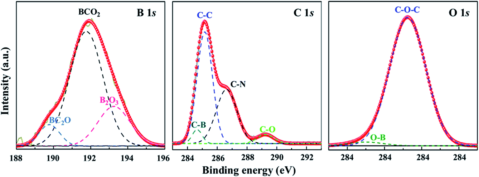 | ||
| Fig. 6 XPS spectra of B 1s, C 1s, and O 1s core levels, respectively. The spectra are deconvoluted by Gaussian fitting (dash curves), indicating possible multibonding information. | ||
The measurements of Vickers hardness (HV) on the high-quality polished surfaces of the produced NPD sample with the 5 wt% B4C additive were accomplished with a standard square-pyramidal diamond indenter. The loading forces were controlled in a range of 0.98 to 9.8 N to create the indentations for obtaining the asymptotic region. The sintered diamond under relatively low P–T conditions (6.5 GPa, 1750–1950 K) showed hardness value ∼42–46 GPa (Fig. S7†), with ∼8 mm in diameter suitable for cutting tools. For direct comparison, the HPHT treated samples at 18 GPa and 2273 K show much higher hardness properties. Fig. 7a shows one typical hardness–load curve of the produced np-diamond with 5 wt% B4C (181010-18). The asymptotic hardness obtained at loads above 5 N reached up to 87 and 90 GPa (Fig. 7b) for the np-diamond with 3 wt% B4C (181010-16) and 5 wt% B4C (181010-18), respectively, indicating a new ultrahard material. This HV value is almost 1.5 times harder than that of the single-crystal cBN and has reached the range of single-crystal diamond.
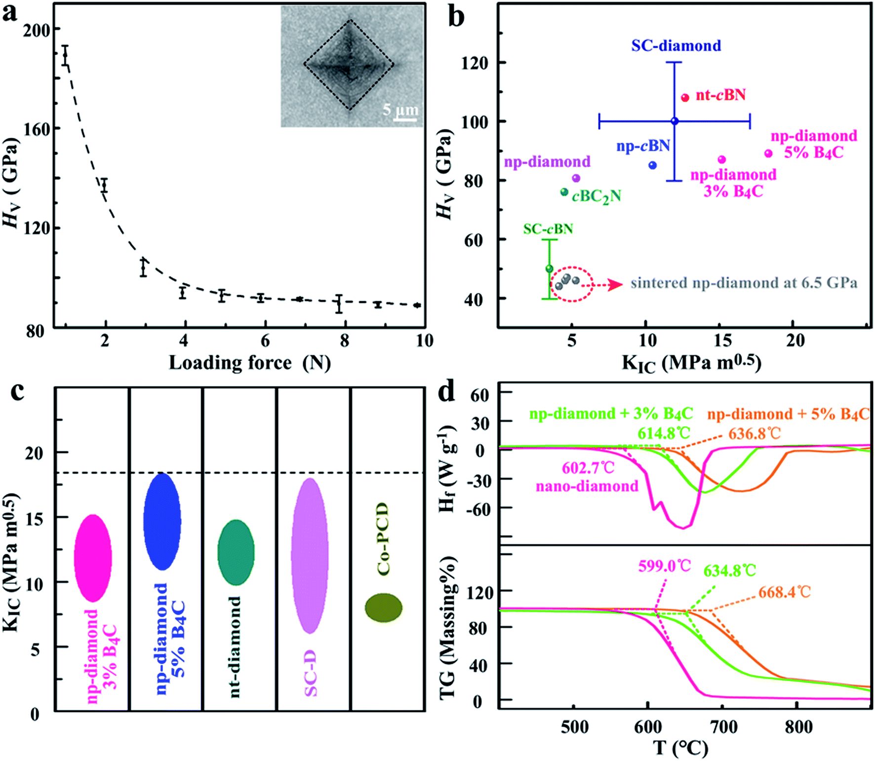 | ||
| Fig. 7 (a) Vickers hardness (HV) of the produced NPD sample with the 5 wt% B4C additive as a function of applied load (F). The right top inset, an optical image of the indentation with cracks produced at a load of 9.8 N. (b) Plot of HV against KIC for recently fabricated superhard diamond and diamond-like material, including BPD diamond with the B4C additive (this work), single-crystal cBN,40 np-cBN,40 nt-diamond,3 single-crystal diamond,6 and cobolt-doped polycrystalline diamond41 for comparision. (c) Comparision of strength for diamond-like materials. (d) Typical thermal stability of the produced NPD with the B4C additive. | ||
Furthermore, it is important to note that no obvious crack was found around the obtained indentations at relatively low loads below 4.8 N while only a little short cracks could be found around the obtained indentations at high loads during hardness measurement, as shown in the top inset of Fig. 7a, indicating the ultra-high fracture toughness of the sintered diamond samples. We employed the high loads in the range of 4.8–9.8 N to create cracks for the fracture toughness determination of the produced np-diamond. The produced typical cracks are shown in Fig. S8.† The determined fracture toughness values are in the range of 8.448–15.18 MPa m0.5 and 10.9–18.37 MPa m0.5 for the np-diamond with 3 wt% B4C (181010-16) and 5 wt% B4C (181010-18), respectively. As shown in Fig. 7c, the maximum fracture toughness value (18.37 MPa m0.5) is even ∼24% higher than that of the hardest known nt-diamond3 (14.8 MPa m0.5) and a little greater than that of the toughest CVD diamond6 (18 MPa m0.5). In addition, we note that the produced np-diamond exhibits high thermal stability (Fig. 7d).
Taking into account the large-scale homogeneity and isotropy, the produced np-diamond with noticeably enhanced strength and toughness in this work can be easily fabricated into arbitrary shape for industrial application. The previous results have proved that the mechanical properties of ultrahard diamond and diamond-like materials can be effectively improved with the assistance of the twinned structure or insertion of relatively soft phases (e.g. cBN) at the grain boundaries.3,13,26–28 Thus, the simultaneous enhancement of fracture toughness and stability in this work primarily depends on the existence of the soft grain boundary phase, B4C domains (shown in Fig. 5), which is of great help in releasing the residual stress formed during the HPHT sintering process. Combining the ultra-hardness and high thermal stability, the successfully enhanced strength in sintered np-diamond by adding B4C in the HPHT treatment environment opens up a novel effective approach in improving and controlling the hardness and stiffness of polycrystalline diamond, which is critical for their further widespread application in the industry and high pressure science.
4. Conclusions
In summary, we fabricated ultrahard np-diamond by directly sintering nano-diamond powders with the B4C additive under HPHT conditions. The average size of the diamond grains is ∼16 nm, which is close to the critical value (typically ∼10–15 nm) for the hardening mechanism of nano-polycrystalline materials by the Hall–Petch effect and quantum confinement effect. The asymptotic hardness of the produced np-diamond with 5 wt% B4C can reach up to 90 GPa. More importantly, the maximum fracture toughness values were found to be 18.37 MPa m0.5, due to the existence of the soft B4C domains at grain boundaries, which is about ∼24% higher than that of the hardest known nt-diamond (14.8 MPa m0.5) and also a little greater than that of the toughest CVD diamond (18 MPa m0.5). Our work provides an improved understanding of the mechanism of function enhancement by the interfaces for the interfaces in polycrystalline materials and a new convenient and low-cost method to fabricate ultrahard and ultra-strong diamond materials.Conflicts of interest
The authors declare no competing financial interest.Acknowledgements
This work was supported by the National Natural Science Foundation of China (11974208, 11804184 and 11704220) and Shandong Provincial Science Foundation (ZR2017BA020, ZR2019BA010 and ZR2019MA054). The authors acknowledge help of Dr Y. B. Wang in the sample preparation and discussion at the University of Chicago.References
- T. Irifune, A. Kurio, S. Sakamoto, T. Inoue and H. Sumiya, Nature, 2003, 421, 599 CrossRef CAS PubMed.
- R. B. Kaner, J. J. Gilman and S. H. Tolbert, Science, 2005, 308, 1268–1269 CrossRef CAS PubMed.
- Q. Huang, D. Yu, B. Xu, W. Hu, Y. Ma, Y. Wang, Z. Zhao, B. Wen, J. He and Z. Liu, Nature, 2014, 510, 250 CrossRef CAS PubMed.
- S. Kunuku, K. J. Sankaran, C.-Y. Tsai, W.-H. Chang, N.-H. Tai, K.-C. Leou and I.-N. Lin, ACS Appl. Mater. Interfaces, 2013, 5, 7439–7449 CrossRef CAS PubMed.
- X. Liu, X. Chen, D. J. Singh, R. A. Stern, J. Wu, S. Petitgirard, C. R. Bina and S. D. Jacobsen, Proc. Natl. Acad. Sci. U. S. A., 2019, 116, 7703–7711 CrossRef CAS PubMed.
- C.-S. Yan, H.-K. Mao, W. Li, J. Qian, Y.-S. Zhao and R. J. Hemley, Phys. Status Solidi A, 2004, 201, R25–R27 CrossRef CAS.
- S. Turner, Y.-G. Lu, S. D. Janssens, F. D. Pieve, D. Lamoen, J. Verbeeck, K. Haenen, P. Wagner and G. V. Tendeloo, Nanoscale, 2012, 4, 5960–5964 RSC.
- S. Mandal, H. A. Bland, J. A. Cuenca, M. Snowball and O. A. Williams, Nanoscale, 2019, 11, 10266–10272 RSC.
- V. Brazhkin, N. Dubrovinskaia, M. Nicol, N. Novikov, R. Riedel, V. Solozhenko and Y. Zhao, Nat. Mater., 2004, 3, 576–577 CrossRef CAS PubMed.
- R. H. Wentorf, R. C. DeVries and F. P. Bundy, Science, 1980, 208, 873–880 CrossRef CAS PubMed.
- X. Liu, Y.-Y. Chang, S. N. Tkachev, C. R. Bina and S. D. Jacobsen, Sci. Rep., 2017, 7, 42921 CrossRef CAS PubMed.
- T. Holz, D. Mata, N. F. Santos, I. Bdikin, A. J. S. Fernandes and F. M. Costa, ACS Appl. Mater. Interfaces, 2014, 6, 22649–22654 CrossRef CAS PubMed.
- B. Li, H. Sun and C. Chen, Nat. Commun., 2014, 5, 4965 CrossRef CAS PubMed.
- G. Li, S. I. Morozov, Q. Zhang, Q. An, P. Zhai and G. J. Snyder, Phys. Rev. Lett., 2017, 119, 215503 CrossRef PubMed.
- R. Yu, H. Wu, J. D. Wang and J. Zhu, ACS Appl. Mater. Interfaces, 2017, 9, 4253–4258 CrossRef CAS PubMed.
- Z. Zhao, B. Xu and Y. Tian, Annu. Rev. Mater. Res., 2016, 46, 383–406 CrossRef CAS.
- V. L. Solozhenko, O. O. Kurakevych and Y. L. Godec, Adv. Mater., 2012, 24, 1540–1544 CrossRef CAS PubMed.
- T. Irifune, K. Kawakami, T. Arimoto, H. Ohfuji, T. Kunimoto and T. Shinmei, Nat. Commun., 2016, 7, 13753 CrossRef CAS PubMed.
- J. Wang, F. Sansoz, C. Deng, G. Xu, G. Han and S. X. Mao, Nano Lett., 2015, 15, 3865–3870 CrossRef CAS PubMed.
- K. Tanigaki, H. Ogi, H. Sumiya, K. Kusakabe, N. Nakamura, M. Hirao and H. Ledbetter, Nat. Commun., 2013, 4, 2343 CrossRef PubMed.
- W. L. Mao, H.-k. Mao, P. J. Eng, T. P. Trainor, M. Newville, C.-c. Kao, D. L. Heinz, J. Shu, Y. Meng and R. J. Hemley, Science, 2003, 302, 425–427 CrossRef CAS PubMed.
- Y. Tian, B. Xu, D. Yu, Y. Ma, Y. Wang, Y. Jiang, W. Hu, C. Tang, Y. Gao, K. Luo, Z. Zhao, L.-M. Wang, B. Wen, J. He and Z. Liu, Nature, 2013, 493, 385 CrossRef CAS PubMed.
- M. Hu, J. He, Z. Zhao, T. A. Strobel, W. Hu, D. Yu, H. Sun, L. Liu, Z. Li, M. Ma, Y. Kono, J. Shu, H.-K. Mao, Y. Fei, G. Shen, Y. Wang, S. J. Juhl, J. Y. Huang, Z. Liu, B. Xu and Y. Tian, Sci. Adv., 2017, 3, e1603213 CrossRef PubMed.
- J. Xiao, J. L. Li, P. Liu and G. W. Yang, Nanoscale, 2014, 6, 15098–15106 RSC.
- J. Narayan, A. Bhaumik, R. Sachan, A. Haque, S. Gupta and P. Pant, Nanoscale, 2019, 11, 2238–2248 RSC.
- B. Li, H. Sun and C. Chen, Phys. Rev. Lett., 2016, 117, 116103 CrossRef PubMed.
- X. J. Li, L. L. He, Y. S. Li, Q. Yang and A. Hirose, ACS Appl. Mater. Interfaces, 2013, 5, 7370–7378 CrossRef CAS PubMed.
- K. J. Sankaran, N. Kumar, J. Kurian, R. Ramadoss, H.-C. Chen, S. Dash, A. K. Tyagi, C.-Y. Lee, N.-H. Tai and I.-N. Lin, ACS Appl. Mater. Interfaces, 2013, 5, 3614–3624 CrossRef CAS PubMed.
- F. A. Almeida, E. Salgueiredo, F. J. Oliveira, R. F. Silva, D. L. Baptista, S. B. Peripolli and C. A. Achete, ACS Appl. Mater. Interfaces, 2013, 5, 11725–11729 CrossRef CAS PubMed.
- C. Chen, Z. Wang, T. Kato, N. Shibata, T. Taniguchi and Y. Ikuhara, Nat. Commun., 2015, 6, 6327 CrossRef CAS PubMed.
- X. Liu, X. Chen, H.-A. Ma, X. Jia, J. Wu, T. Yu, Y. Wang, J. Guo, S. Petitgirard, C. R. Bina and S. T. Jacobsen, Sci. Rep., 2016, 6, 30518 CrossRef CAS PubMed.
- B. Yang, X. Peng, C. Huang, D. Yin, H. Xiang and T. Fu, ACS Appl. Mater. Interfaces, 2018, 10, 42804–42811 CrossRef CAS PubMed.
- K. M. Reddy, J. Guo, Y. Shinoda, T. Fujita, A. Hirata, J. Singh, J. W. McCauley and M. W. Chen, Nat. Commun., 2012, 3, 1052 CrossRef PubMed.
- K. M. Reddy, P. Liu, A. Hirata, T. Fujita and M. W. Chen, Nat. Commun., 2013, 4, 2483 CrossRef PubMed.
- E. O. Hall, Proc. Phys. Soc., London, Sect. B, 1951, 64, 747–753 CrossRef.
- S. Jacques, A. Guette, X. Bourrat, F. Langlais, C. Guimon and C. Labrugere, Carbon, 1996, 34, 1135–1143 CrossRef CAS.
- G. Chang, F. Sun, L. Wang, Z. Che, X. Wang, J. Wang, M. J. Kim and H. Zhang, ACS Appl. Mater. Interfaces, 2019, 11, 26507–26517 CrossRef CAS PubMed.
- X. Wang, Y. Ishii, A. R. Ruslinda, M. Hasegawa and H. Kawarada, ACS Appl. Mater. Interfaces, 2012, 4, 3526–3534 CrossRef CAS PubMed.
- L. Ci, L. Song, C. Jin, D. Jariwala, D. Wu, Y. Li, A. Srivastava, Z. F. Wang, K. Storr, L. Balicas, F. Liu and P. M. Ajayan, Nat. Mater., 2010, 9, 430 CrossRef CAS PubMed.
- M. P. D'Evelyn and T. Taniguchi, Diamond Relat. Mater., 1999, 8, 1522–1526 CrossRef.
- A. Lammer, Mater. Sci. Technol., 1988, 6, 949–955 CrossRef.
Footnote |
| † Electronic supplementary information (ESI) available. See DOI: 10.1039/c9na00699k |
| This journal is © The Royal Society of Chemistry 2020 |