DOI:
10.1039/C9NA00528E
(Paper)
Nanoscale Adv., 2020,
2, 1059-1065
A self-encapsulated broadband phototransistor based on a hybrid of graphene and black phosphorus nanosheets†
Received
23rd August 2019
, Accepted 20th December 2019
First published on 20th December 2019
Abstract
A phototransistor based on a hybrid of graphene and BP nanosheets with a facile fabrication method and remarkable performance is presented. Unlike previously reported single BP flake-based devices, this phototransistor employs diverse BP nanosheets with different sizes and layer numbers. The wet transfer process of graphene is exploited to integrate the liquid-exfoliated BP nanosheets into the device smoothly. Due to the diversity of BP nanosheets, the device demonstrates a broadband photo-response in the spectrum from 360 nm to 785 nm. The photo-response mechanism is revealed to be the photogating effect caused by the discrete BP nanosheets adsorbed on graphene. The phototransistor has a responsivity of 7.7 × 10³ A W−1 in the near-UV region with a wide conductive channel of 200 μm. Moreover, the simplified wet transfer process of graphene leaves a self-encapsulated layer of PMMA on the as-prepared device, inducing a good atmospheric stability in the device. This report provides a valid, implantable, and facile strategy to apply BP nanosheets in a broadband, high-performing and air-stable photodetector.
Introduction
Two dimensional (2D) materials have been widely investigated for their application in photodetectors due to their excellent optoelectronic properties.1–8 Therein, black phosphorus (BP), a layered single crystal with an orthorhombic structure, is of particular importance as it has outstanding merits surpassing other 2D materials including a direct bandgap regardless of the layer number and a wide tunable range of the bandgap from 0.33 eV to 2 eV depending on the layer number.9–13 A battery of photodetectors based on exfoliated BP flakes have been reported.14–23 These devices demonstrate distinct performance depending on the BP layer number, channel length, sensing wavelength, temperature etc. For example, the record-high responsivity of a BP-based photodetector is reported by M. Huang et al. by using BP nanosheets of 15 layers and a conductive channel of 100 nm, reaching up to 7 × 10⁶ A W−1 at a 20 K sensing light of 900 nm.19 Responsivity will decrease to a moderate level of 104 A W−1 when the channel length increases up to 1 μm. Obviously, an ultra-narrow channel length, which will induce a limited photosensitive area, along with harsh fabrication conditions would hinder the practical application of this kind of device. To boost the performance of the BP-based phototransistor, an alternative strategy is to employ a graphene–BP hybrid structure. The ultrahigh carrier mobility in graphene and the transparency due to its ultrathin thickness enable monolayer graphene a good conductor for photo-induced carriers.2,24 Lots of light harvesting materials including quantum dots, organic–inorganic perovskites,25 and graphene-like two dimensional materials26–28 have been integrated in order to fabricate a high performance phototransistor, achieving a responsivity of up to 108 A W−1.28 Based on a graphene–BP hybrid structure, Y. Liu et al. and J. Xu et al. successively reported two kinds of phototransistors, in which graphene is used as the conductive layer of the transistor while the BP nanosheet as the light harvester.29,30 Due to different layer numbers of BP nanosheets (70 layers for the former and 6 layers for the latter), these two devices can sense infrared light with a responsivity of 3.3 × 10³ A W−1 and visible light with a responsivity of 55.75 A W−1, respectively.
So far, advancements in BP-based photodetectors are based on layered BP single crystals mechanically exfoliated from bulk materials. The complexity of mechanical exfoliation would be a considerable barrier towards the practical application of such a kind of device, as the large-scale growth technology of BP is not available yet.31 Moreover, atmospheric stability issue of the devices is not clearly addressed in previous reports. Considering that BP is very unstable in air,10,32,33 the atmospheric stability of the device must be taken into account for relevant exploration. Especially, in the report by Liu et al. a bottom-BP–top-graphene configuration is employed in a phototransistor based on a graphene–BP hybrid. The graphene atop the BP nanosheet isolates BP from air, inducing a good atmospheric stability of the device.30 Nevertheless, graphene itself is sensitive to air also, suggesting the necessity of additional encapsulation. In this work, a phototransistor based on the graphene–BP nanosheet hybrid is presented. The BP nanosheets with a range of layer numbers are adsorbed onto graphene during its PMMA-assisted wet-transfer process. The wet-transfer process is simplified by reserving the PMMA layer on graphene. Thanks to the wide distribution of the layer number of BP nanosheets, the phototransistor demonstrates a broadband detection ability of light from 360 nm to 785 nm, covering the spectrum from near-ultraviolet to visible. The device shows a responsivity of 7.7 × 10³ A W−1 for 360 nm illumination with a wide channel length of 200 μm. Moreover, the reserved PMMA layer plays an encapsulation role, inducing a benign atmospheric stability of the device.
Experimental
BP nanosheet preparation
The aqueous solution of BP nanosheets was prepared through a reported liquid exfoliation technique with modification.34 Generally, bulk BP (40 mg) was added to NMP (40 mL) in a conical tube (50 mL). With temperature kept below 25 °C using a water-cooling coil, the mixture was ultrasonicated using a sonic tip with a power of 650 W. The ultrasonication lasted for 4 hours with on/off cycles of 2s/2s. The obtained turbid liquid was centrifuged for 20 min at 3000 rpm. The top half of the supernatant was drawn and filtered with an organic membrane with a hole diameter of 150 nm. The filtered residue was dried at 100 °C in a vacuum drying oven and then dispersed in DI-water for use.
Device fabrication
Si/SiO2 wafer with heavily p-doped Si and SiO2 of 300 nm thickness was used as the substrate. Two Au electrodes were thermally evaporated on the substrate defining a channel with a length of 0.2 mm and a width of 2 mm. A graphene–BP film with a PMMA protection layer was prepared and transferred atop the substrate using a modified classical wet transfer method.35 Specifically, the CVD-grown graphene on a Cu coil was purchased from 6Carbon Technology (Shenzhen). PMMA solution in anisole was spin-coated on the coil with graphene. The Cu coil was then etched in ammonium persulfate solution in water. The floating PMMA–graphene was transferred to the aqueous solution of BP nanosheets and kept for one hour before its final transfer to the substrate. The device was annealed at 60 °C for 30 min in a glovebox filled with nitrogen before measurement. The same graphene–BP film was transferred onto a glass substrate for absorbance measurement. The same graphene–BP film was transferred onto a Si substrate with the PMMA layer washed off later by acetone and used as the SEM sample.
Characterization
The absorbance spectra were measured using a Cary 60 system with tunable wavelengths. The SEM image was obtained on a Netherlands instrument Phenom Pro microscope. The TEM and HRTEM images were acquired on a Tecnai G2 F30 high-resolution transmission electron microscope. Raman measurement was conducted on a Renishaw InVia Raman microscope with an excitation laser wavelength of 532 nm. The AFM images were obtained using a Bruker Dimension Icon atomic force microscope. Devices were measured using a combination of a Keithley 4200 semiconductor analysis system and a probe station in either glovebox filled with N2 or the atmosphere. The photo-response of the devices was characterized under the illumination of CHI continuous lasers with wavelengths of 360, 405, 532, and 785 nm.
Results and discussion
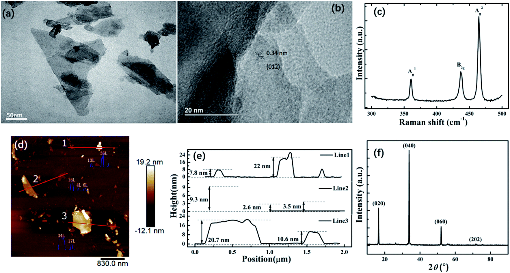
The BP nanosheets dispersed in water are prepared from the BP bulk using a liquid exfoliation technique reported before.34Fig. 1a is the transmission electron microscope (TEM) image of the BP nanosheets, revealing their nonuniform sizes. The high resolution TEM image in Fig. 1b demonstrates the (012) crystal lattice of BP.36 The X-ray diffraction pattern in Fig. 1c further confirms the orthorhombic lattice structure of the BP nanosheets. The Raman spectrum of a BP nanosheet on a silicon substrate with an excitation of 532 nm laser is shown in Fig. 1d. The peaks at 362, 440, and 467 cm−1 correspond to the vibration modes of the BP nanosheet crystal lattice named after A1g, B2g, and A2g, respectively.37 The AFM images of BP nanosheets on the substrate are shown in Fig. 1d. It reveals that besides the nonuniform size, the BP nanosheets have different thicknesses, corresponding to different layer numbers. The contours along with three lines are profiled in Fig. 1f to probe the thickness of the BP nanosheets overlapped. The corresponding layer numbers of the nanosheets along with the three lines are shown in Fig. 1e. According to the BP monolayer thickness of ∼0.6 nm, the probed BP nanosheets have a layer number between 4–36.38 Note that this layer number range must not cover all BP nanosheets in the solution. It is very probable that monolayer BP exists according to the previous report on the liquid exfoliation technique.34 It is well known that the bandgap of BP varies from 0.3 to 2.0 eV with the layer number decreasing from more than ten to one.10 Therefore, the BP nanosheets used in this work have widely dispersed electronic band gaps, which are supposed to enable the efficient broadband photodetection ability of the presented phototransistor.
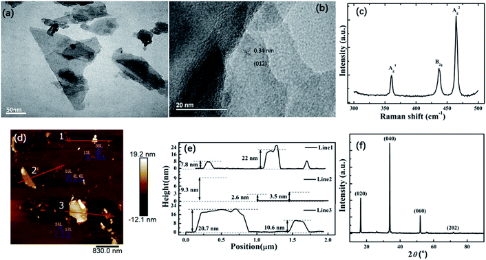 |
| | Fig. 1 Characterization of BP nanosheets. (a) TEM image; (b) HRTEM image; (c) Raman spectrum excited by a laser of 532 nm; (d) AFM image. The layer numbers of BP nanosheets are denoted by three marked lines; (e) the thickness profiles along with the three marked lines in the left figure. (f) XRD spectrum. | |
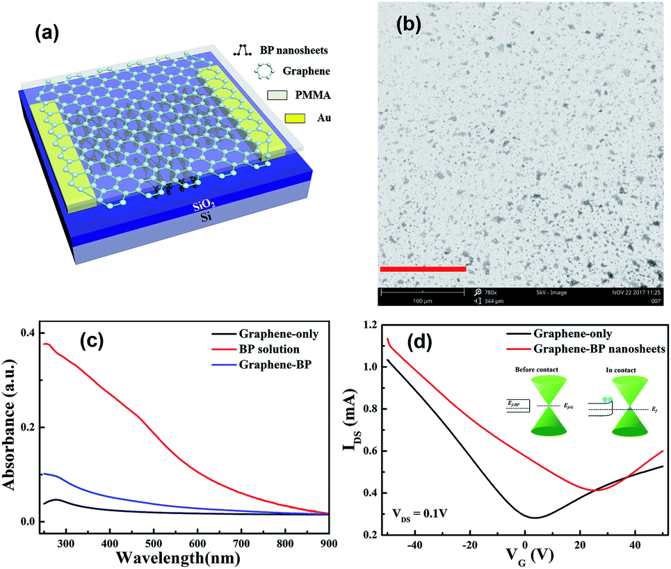
A phototransistor based on graphene–BP nanosheet hybrids (graphene–BP) is fabricated with a structure as illustrated in Fig. 2a. First, a heavily n-doped silicon substrate with a silica surface layer of 300 nm is cleaned and treated with O2 plasma for use. Then two Au electrodes are thermally evaporated onto the substrate through a shadow mask defining a conducting channel with a width/length of 2/0.2 mm. CVD-grown monolayer graphene on a Cu coil was commercially purchased. The graphene–BP film is prepared using a modified classical wet-transfer method.35 Specifically, a PMMA layer is deposited on the graphene for protection. The Cu coil is etched in ammonium persulfate solution. The floating PMMA–graphene membrane is transferred to the aqueous solution of BP nanosheets and kept for one hour before its final transfer to the substrate. Graphene in this very step would adsorb BP nanosheets, forming a graphene–BP nanosheet hybrid film. The hybrid film is then transferred onto the electrode-deposited substrate giving a phototransistor. The monolayer properties and good crystallinity of graphene are further verified by the Raman spectrum of a pure graphene on the Si/SiO2 substrate prepared using the same transfer method except for the existence of BP, as shown in Fig. S1.†35 The scanning electron microscope (SEM) image of the hybrid film with the PMMA layer washed off is shown in Fig. 2b, which reveals a discrete adsorption of BP nanosheets on graphene. The UV-Vis absorbance spectra of the graphene film with PMMA, BP nanosheet solution, and graphene–BP film with PMMA are shown in Fig. 2c. The results reasonably reveal the universal enhancement of absorbance after graphene adsorbed the BP nanosheets in the measured range, thanks to the wide spectral absorption of the BP nanosheets. It is worth noting that the enhancement in the ultraviolet side is less than that in the long wavelength side. The reason is speculated to be that the percentage of BP nanosheets with more layers, which have a smaller band gap, is larger in the adsorbed film than in solution. A graphene-only device with the same device configuration but excluding the BP nanosheets was fabricated for comparison. The transfer curves of the graphene–BP and graphene-only devices were obtained in the dark and are shown in Fig. 2d. The Dirac point of the transfer curve of the graphene–BP device locates at a more positive position than the graphene-only device, implying a p-doping effect caused by the BP nanosheets to graphene. This is understandable as BP is a p type semiconductor with a lower Fermi level than graphene.10,11,38
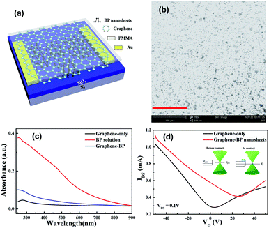 |
| | Fig. 2 (a) Schematic diagram of the graphene–BP phototransistor; (b) SEM image of the graphene–BP hybrid film, scale bar: 100 μm; (c) UV-Vis absorbance spectra of graphene (with PMMA), BP solution, and the graphene–BP film (with PMMA); (d) transfer characterization of transistors based on graphene and graphene–BP in the dark. The inset is the illustration of the p-doping effect on graphene induced by BP. | |
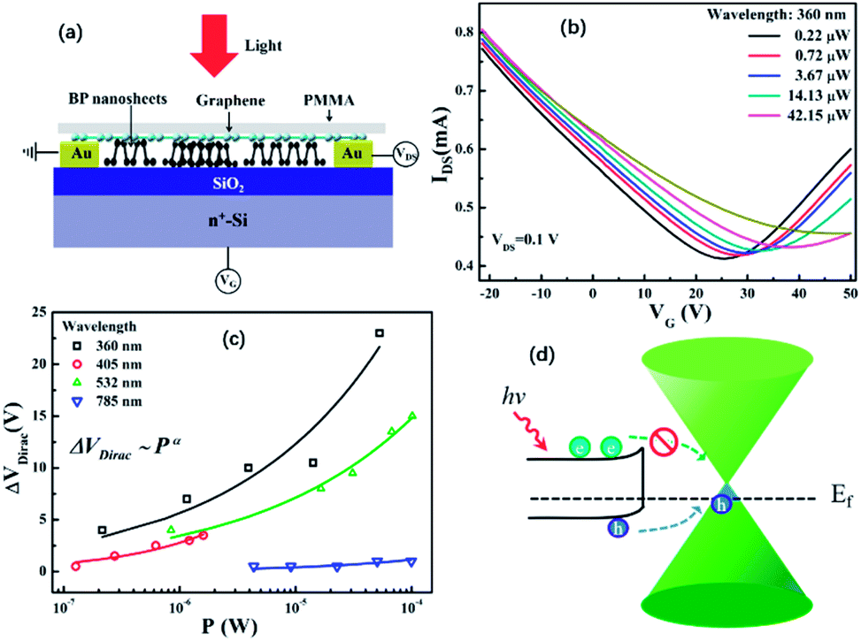
The graphene–BP phototransistor was characterized under light illumination with the measurement configuration shown in Fig. 3a. Four lasers with wavelengths of 360 nm, 405 nm, 532 nm, and 785 nm and a tunable light intensity were used. The transfer characteristics of the device under 360 nm illumination with different radiant fluxes are shown in Fig. 3b. The same characteristics for 405, 532, and 785 nm are shown in Fig. S2.† The transfer curve positively shifts along with the increase of the radiant flux for all the four lights. In comparison, the graphene-only device shows no photo-response in its transfer characteristics with even larger VDS under the illumination of four lasers each with the largest radiant fluxes, as shown in Fig. S2d.† Therefore, the photo-response should be primarily caused by the BP nanosheets. The enhanced p-doping effect along with the increase of radiant flux imply a net hole transfer from BP to graphene. The changes in the Dirac points (ΔVDirac) along with the radiant flux (P) are plotted in Fig. 3c for all four lasers. The curves can be fitted well with the following equation:
where
A and
α are constants for each laser and
P is the radiant flux. The
α values obtained by fitting the experimental data are listed in
Table 1. It is worth noting that this relationship has been widely observed in photogating phototransistors.
35,39,40 Considering that the fermi level of graphene lies between the band gaps of BP, the photo-response scenario is illustrated in
Fig. 3d. The BP nanosheets are responsible for the light harvesting. Both the photo-induced electrons and holes in BP should be able to transfer from BP to graphene. Nevertheless, due to the energy barrier in the graphene–BP interface, the transfer of electrons would be either forbidden or retarded, inducing net electron residues in BP. This will lead to an extra negative bias to graphene, which corresponds to Δ
VDirac. Note that the shift of the transfer curve in the high negative voltage region is smaller than the Dirac point, which may be due to the high hole density in graphene induced by the hole injection from BP.
 |
| | Fig. 3 (a) Schematic diagram of the cross section of the graphene–BP phototransistor; (b) transfer characteristics of the phototransistor under illumination of 360 nm light with different radiant flux; (c) the changes of the Dirac point as a function of radiant flux for light with different wavelengths. Dots are the experimental data. Lines are the fitting curves with power functions; (d) illustration of the photo-response mechanism. | |
Table 1 Indexes α and β obtained by fitting ΔVG–P and R–P curves with power functions
| Wavelength |
360 nm |
405 nm |
532 nm |
785 nm |
|
α
|
0.34 |
0.54 |
0.32 |
0.45 |
|
β
|
−0.73 |
−0.51 |
−0.76 |
−0.56 |
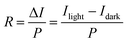
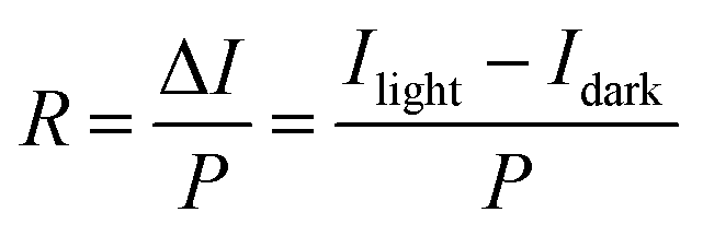
The output characteristics of the graphene–BP phototransistor were measured under different light illuminations with a VG of 0 V. From the output results, the responsivity (R) is calculated with R defined as:
| |  | (2) |
where Δ
I is the photocurrent,
Ilight is the channel current under light illumination, and
Idark is the channel current in the dark. Five representative
R–
VDS curves with different radiant fluxes are plotted and shown in Fig. S3
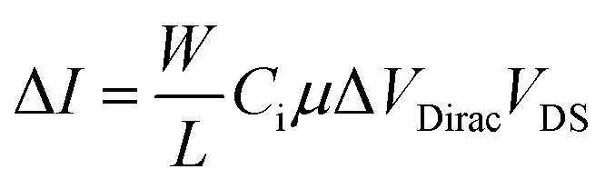
† for each light illumination. The curves of responsivity as a function of radiant flux for different light illuminations are plotted in
Fig. 4a. Notice that the photocurrent Δ
I is given by:
| |  | (3) |
where
W and
L are the width and length of the channel,
Ci the capacitance of the gate dielectric per unit area, and
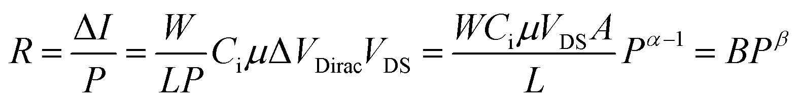
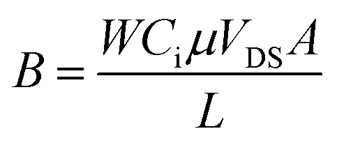
μ the carrier mobility. Considering
eqn (1) and
(3), the responsivity can be given by:
| |  | (4) |
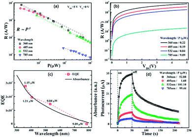 |
| | Fig. 4 (a) Relationships of responsivity and radiant flux (R–P) for different light sources. The responsivity data are abstracted from the output characteristics. Dots are the experimental data and dashed lines are the fitting curves with power functions; (b) responsivities as a function of VDS (R–VDS, VG = 0) for different light sources, each with the lowest intensity; (c) absorbance spectrum of the graphene–BP film and the spectral distribution of EQE of the graphene–BP phototransistor; (d) dynamic behavior of the photocurrent at a VG of 0 V and a VDS of 0.1 V for different light sources each with the highest intensity and an illumination duration of 50 s. | |
Therein,  is a constant, and α − 1 = β. Fig. 4a demonstrates the good power function relationships between R and P, with different indexes for different lasers. The fitting results of β are listed in Table 1. The experimental data of α and β are in good accordance with the theoretical data with a tolerable error. The output and transfer characteristics of the device consistently confirm the photogating mechanism of the photo-response. The responsivity increases with the decrease of radiant flux and the increase of VDS. Fig. 4b shows the curves of responsivity along with VDS for four different lasers each with the lowest irradiance. At the largest VDS of 5 V, the device has the largest responsivity of 7.7 × 10³ A W−1 for 360 nm illumination with a radiant flux of 0.22 μW. It is worth noting that, first, the channel length of the device is 200 μm, which is very larger than those previously reported for BP-based photodetectors.14–23 Second, graphene is not covered by BP nanosheets completely, unlike other analogous photodetectors fabricated based on the hybrid of graphene and layered BP single crystal BP.29,30 These imply the superiority and huge potential of the presented device. Fig. 3b shows the decrease of responsivity with the increase of wavelength, especially a sharp drop at 785 nm, reaching 21 A W−1 with a radiant flux of 9.09 μW. To gain more insights into the broadband response ability of the device, the external quantum efficiencies (EQEs) at VDS of 5 V and VG of 0 V for the four lasers are calculated using the equation EQE = Rhν/e, where h is the Planck constant, ν is the light frequency, and e is the elementary charge. Considering that the EQE relies on radiant flux intensively, the EQEs for different lights are calculated using the data with most comparable radiant fluxes, mimicking the absorbance measurement conditions. The results are plotted along with wavelength and shown in Fig. 4c. The trend of the curve resembles the absorbance spectrum of the BP–graphene hybrid film very much. This result manifests a broadband response ability of the device rooting in the light harvesting by the hybrid film.
The dynamic responses of the phototransistor to lights were characterized and are shown in Fig. 4d. The highest light irradiance and a long illumination duration of 50 s were used to reveal the process clearly. The photocurrents keep increasing with the increase of light illumination. When the light is turned off, the photocurrents decay sharply first, and then decrease slowly. The ascendant and descendant processes of the photocurrent are fitted with exponential functions of  and
and  , respectively. Therein, τa1 and τd1 are separately the time constants of fast rise and decay, and τa2 and τd2 are the slow rise and decay. The fitting parameters of these time constants are listed in Table 2. The fast time constant should be associated with the carrier transfer from BP to graphene, and the slow time constant is usually attributed to the charge transport process in the light sensitizers,35,39 which are BP nanosheets, especially the multilayer BP nanosheets in this study. Notice that τd1 and τd2 are larger than τa1 and τa2, respectively. We speculate the reason is that the energy barrier at the interface of BP and graphene hinders the inverted charge transfer, thus slowing down the charge recombination process.
Table 2 Time constants obtained by fitting the dynamic photo-response with exponential functions
| wavelength |
360 nm |
405 nm |
532 nm |
785 nm |
|
τ
a1
|
3.5 s |
3.2 s |
4.3 s |
3.0 s |
|
τ
a2
|
20.5 s |
25.6 s |
27.1 s |
29.6 s |
|
τ
b1
|
7.9 s |
6.2 s |
7.9 s |
7.8 s |
|
τ
b2
|
171.6 s |
87.8 s |
115.7 s |
216.8 s |
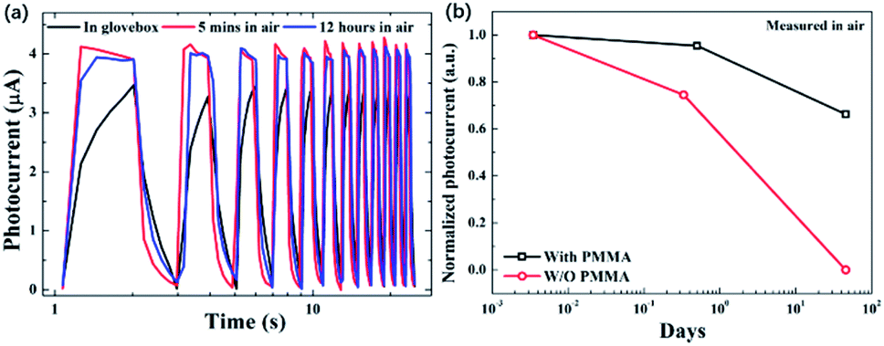
BP has been proved to be very unstable in the atmosphere due to its robust reactions with oxygen and water vapor, which can be accelerated by photons.10 This will be a big obstacle to apply BP in phototransistors. Graphene has been reported as an effective encapsulation layer when covering upon BP in phototransistors.30 This study pushes this strategy further by sparing the step of washing off the PMMA film on graphene, which is a built-in layer in the wet transfer process of graphene. With this design, the graphene–BP phototransistor is self-encapsulated by the PMMA film. To evaluate the effect of this encapsulation, the transient photo-response behavior of the device was characterized under a multi-cycle on/off illumination of 532 nm light in terms of the exposure duration to air. The result in Fig. 5a shows that with 5 minutes exposure to air, the photocurrent has a little increase. This can be ascribed to the p-doping of graphene induced by the oxygen adsorption, which would help leveling the valence band of BP and the femi level of graphene,41 facilitating hole transfer from BP to graphene. Thereafter, the photocurrent remains constant after 12 hours exposure to air, implying a good device stability in air. To clarify the role of the PMMA layer, a control device with PMMA washed off was prepared as well. The photocurrent of the devices with and without PMMA was monitored using the same measurement protocol in Fig. 5a, in terms of the air exposure duration of 5 min, 12 hours, and 45 days. The result is shown in Fig. 5b. The photocurrent of the device without PMMA has a very faster decay than the device with PMMA, falling to 0 at the 45th day. On the other hand, the PMMA device still holds 65% of its initial photocurrent at the 45th day. This result clearly demonstrates that the PMMA layer can prevent the deterioration of BP as an effective encapsulation layer.
 |
| | Fig. 5 (a) Photocurrent of the device under a multicycle on/off illumination of 532 nm light at a VG of 0 V and a VDS of 0.1 V. The three measurements were carried out subsequently along with the increased exposure duration in the atmosphere; (b) photocurrent stabilities of devices with and without PMMA layers after exposure to the atmosphere for different times. | |
Conclusions
In summary, a phototransistor based on a hybrid of graphene and BP nanosheets is fabricated with a facile process taking advantage of the wet transfer technology of graphene. The integrated BP nanosheets have a wide range of thickness, inducing a broadband photo-response of the device in the spectrum from 360 nm to 785 nm. The device demonstrates a responsivity of 7.7 × 10³ A W−1 to a light of 360 nm, despite a wide channel length of 200 μm. The photo-response mechanism is revealed to be the photogating effect due to the light harvesting by BP. Moreover, the as-prepared device is self-encapsulated by a PMMA layer, which introduces an excellent atmospheric stability in the device.
Conflicts of interest
There are no conflicts to declare.
Acknowledgements
Z. H. S. acknowledges the financial support from the National Natural Science Foundation of China (grant no. 61505108) and Natural Science Foundation of Guangdong Province (grant no. 2019A1515011367 and 2016A030310055). G. G. Z. acknowledges the financial support from the National Natural Science Foundation of China (grant no. 61805162).
Notes and references
- C. H. Liu, Y. C. Chang, T. B. Norris and Z. H. Zhong, Nat. Nanotechnol., 2014, 9, 273–278 CrossRef CAS PubMed.
- J. H. Li, L. Y. Niu, Z. J. Zheng and F. Yan, Adv. Mater., 2014, 26, 5239–5273 CrossRef CAS PubMed.
- F. H. L. Koppens, T. Mueller, P. Avouris, A. C. Ferrari, M. S. Vitiello and M. Polini, Nat. Nanotechnol., 2014, 9, 780–793 CrossRef CAS PubMed.
- Z. Li, H. Qiao, Z. Guo, X. Ren, Z. Huang, X. Qi, S. C. Dhanabalan, J. S. Ponraj, D. Zhang, J. Li, J. Zhao, J. Zhong and H. Zhang, Adv. Funct. Mater., 2018, 28, 1705237 CrossRef.
- Z. Huang, W. Han, H. Tang, L. Ren, D. S. Chander, X. Qi and H. Zhang, 2D Mater., 2015, 2, 035011 CrossRef.
- Z. Xie, C. Xing, W. Huang, T. Fan, Z. Li, J. Zhao, Y. Xiang, Z. Guo, J. Li, Z. Yang, B. Dong, J. Qu, D. Fan and H. Zhang, Adv. Funct. Mater., 2018, 28, 1705833 CrossRef.
- Q. Ou, Y. Zhang, Z. Wang, J. A. Yuwono, R. Wang, Z. Dai, W. Li, C. Zheng, Z. Q. Xu, X. Qi, S. Duhm, N. V. Medhekar, H. Zhang and Q. Bao, Adv. Mater., 2018, 30, e1705792 CrossRef PubMed.
- Y. Zhang, C.-K. Lim, Z. Dai, G. Yu, J. W. Haus, H. Zhang and P. N. Prasad, Phys. Rep., 2019, 795, 1–51 CrossRef CAS.
- V. Tran, R. Soklaski, Y. F. Liang and L. Yang, Phys. Rev. B: Condens. Matter Mater. Phys., 2014, 89, 235319 CrossRef.
- F. Xia, H. Wang, J. C. M. Hwang, A. H. C. Neto and L. Yang, Nat. Rev. Phys., 2019, 1, 306–317 CrossRef.
- Y. Q. Cai, G. Zhang and Y. W. Zhang, Sci. Rep., 2014, 4, 6677 CrossRef CAS PubMed.
- H. Mu, Z. Wang, J. Yuan, S. Xiao, C. Chen, Y. Chen, Y. Chen, J. Song, Y. Wang, Y. Xue, H. Zhang and Q. Bao, ACS Photonics, 2015, 2, 832–841 CrossRef CAS.
- Z. Li, H. Xu, J. Shao, C. Jiang, F. Zhang, J. Lin, H. Zhang, J. Li and P. Huang, Appl. Mater. Today, 2019, 15, 297–304 CrossRef.
- X. L. Chen, X. B. Lu, B. C. Deng, O. Sinai, Y. C. Shao, C. Li, S. F. Yuan, V. Tran, K. Watanabe, T. Taniguchi, D. Naveh, L. Yang and F. N. Xia, Nat. Commun., 2017, 8, 1672 CrossRef PubMed.
- M. Engel, M. Steiner and P. Avouris, Nano Lett., 2014, 14, 6414–6417 CrossRef CAS PubMed.
- Q. S. Guo, A. Pospischil, M. Bhuiyan, H. Jiang, H. Tian, D. Farmer, B. C. Deng, C. Li, S. J. Han, H. Wang, Q. F. Xia, T. P. Ma, T. Mueller and F. N. Xia, Nano Lett., 2016, 16, 4648–4655 CrossRef CAS PubMed.
- C. X. Hu, Q. Xiao, Y. Y. Ren, M. Zhao, G. H. Dun, H. R. Wu, X. Y. Li, Q. Q. Yang, B. Sun, Y. Peng, F. Yan, Q. Wang and H. L. Zhang, Adv. Funct. Mater., 2018, 28, 1805311 CrossRef.
- L. Huang, B. W. Dong, X. Guo, Y. H. Chang, N. Chen, X. Huang, W. G. Liao, C. X. Zhu, H. Wang, C. Lee and K. W. Ang, ACS Nano, 2019, 13, 913–921 CrossRef CAS PubMed.
- M. Q. Huang, M. L. Wang, C. Chen, Z. W. Ma, X. F. Li, J. B. Han and Y. Q. Wu, Adv. Mater., 2016, 28, 3481–3485 CrossRef CAS PubMed.
- J. Wu, G. K. W. Koon, D. Xiang, C. Han, C. T. Toh, E. S. Kulkarni, I. Verzhbitskiy, A. Carvalho, A. S. Rodin, S. P. Koenig, G. Eda, W. Chen, A. H. C. Neto and B. Ozyilmaz, ACS Nano, 2015, 9, 8070–8077 CrossRef CAS PubMed.
- N. Youngblood, C. Chen, S. J. Koester and M. Li, Nat. Photonics, 2015, 9, 247–252 CrossRef CAS.
- N. Youngblood and M. Li, Appl. Phys. Lett., 2017, 110, 051102 CrossRef.
- X. Zou, Y. Li, G. Tang, P. You and F. Yan, Small, 2019, 15, 1901004 CrossRef PubMed.
- Z. Sun and H. Chang, ACS Nano, 2014, 8, 4133–4156 CrossRef CAS PubMed.
- Z. H. Sun, L. Aigouy and Z. Y. Chen, Nanoscale, 2016, 8, 7377–7383 RSC.
- W. J. Yu, Y. Liu, H. L. Zhou, A. X. Yin, Z. Li, Y. Huang and X. F. Duan, Nat. Nanotechnol., 2013, 8, 952–958 CrossRef CAS PubMed.
- H. J. Tan, W. S. Xu, Y. W. Sheng, C. S. Lau, Y. Fan, Q. Chen, M. Tweedie, X. C. Wang, Y. Q. Zhou and J. H. Warner, Adv. Mater., 2017, 29, 1702917 CrossRef PubMed.
- K. Roy, M. Padmanabhan, S. Goswami, T. P. Sai, G. Ramalingam, S. Raghavan and A. Ghosh, Nat. Nanotechnol., 2013, 8, 826–830 CrossRef CAS PubMed.
- J. Xu, Y. J. Song, J. H. Park and S. Lee, Solid-State Electron., 2018, 144, 86–89 CrossRef CAS.
- Y. Liu, B. N. Shivananju, Y. S. Wang, Y. P. Zhang, W. Z. Yu, S. Xiao, T. Sun, W. L. Ma, H. R. Mu, S. H. Lin, H. Zhang, Y. R. Lu, C. W. Qiu, S. J. Li and Q. L. Bao, ACS Appl. Mater. Interfaces, 2017, 9, 36137–36145 CrossRef CAS PubMed.
- D. Wang, P. Yi, L. Wang, L. Zhang, H. Li, M. Lu, X. Xie, L. Huang and W. Huang, Front. Chem., 2019, 7, 21 CrossRef CAS PubMed.
- R. A. Doganov, E. C. T. O'Farrell, S. P. Koenig, Y. Yeo, A. Ziletti, A. Carvalho, D. K. Campbell, D. F. Coker, K. Watanabe, T. Taniguchi, A. H. C. Neto and B. Özyilmaz, Nat. Commun., 2015, 6, 6647 CrossRef CAS PubMed.
- S. X. Liu, Z. J. Li, Y. Q. Ge, H. D. Wang, R. Yue, X. T. Jiang, J. Q. Li, Q. Wen and H. Zhang, Photonics Res., 2017, 5, 662–668 CrossRef CAS.
- X. H. Ren, Z. J. Li, Z. Y. Huang, D. Sang, H. Qiao, X. Qi, J. Q. Li, J. X. Zhong and H. Zhang, Adv. Funct. Mater., 2017, 27, 1606834 CrossRef.
- Z. Sun, Z. Liu, J. Li, G.-a. Tai, S.-P. Lau and F. Yan, Adv. Mater., 2012, 24, 5878–5883 CrossRef CAS PubMed.
- W. Guo, H. Song and S. Yan, Opt. Commun., 2018, 406, 91–94 CrossRef CAS.
- Y. Xu, Z. Wang, Z. Guo, H. Huang, Q. Xiao, H. Zhang and X.-F. Yu, Adv. Opt. Mater., 2016, 4, 1223–1229 CrossRef CAS.
- H. Liu, A. T. Neal, Z. Zhu, Z. Luo, X. Xu, D. Tománek and P. D. Ye, ACS Nano, 2014, 8, 4033–4041 CrossRef CAS PubMed.
- F. Yan, J. H. Li and S. M. Mok, J. Appl. Phys., 2009, 106, 1606834 Search PubMed.
- C. Hu, D. D. Dong, X. K. Yang, K. K. Qiao, D. Yang, H. Deng, S. J. Yuan, J. Khan, Y. Lan, H. S. Song and J. Tang, Adv. Funct. Mater., 2017, 27, 1603605 CrossRef.
- S. Ryu, L. Liu, S. Berciaud, Y.-J. Yu, H. Liu, P. Kim, G. W. Flynn and L. E. Brus, Nano Lett., 2010, 10, 4944–4951 CrossRef CAS PubMed.
Footnote |
| † Electronic supplementary information (ESI) available. See DOI: 10.1039/c9na00528e |
|
| This journal is © The Royal Society of Chemistry 2020 |
Click here to see how this site uses Cookies. View our privacy policy here. 
 Open Access Article
 This Open Access Article is licensed under a Creative Commons Attribution-Non Commercial 3.0 Unported Licence
 b and
Zhenhua
Sun
b and
Zhenhua
Sun

 is a constant, and α − 1 = β. Fig. 4a demonstrates the good power function relationships between R and P, with different indexes for different lasers. The fitting results of β are listed in Table 1. The experimental data of α and β are in good accordance with the theoretical data with a tolerable error. The output and transfer characteristics of the device consistently confirm the photogating mechanism of the photo-response. The responsivity increases with the decrease of radiant flux and the increase of VDS. Fig. 4b shows the curves of responsivity along with VDS for four different lasers each with the lowest irradiance. At the largest VDS of 5 V, the device has the largest responsivity of 7.7 × 10³ A W−1 for 360 nm illumination with a radiant flux of 0.22 μW. It is worth noting that, first, the channel length of the device is 200 μm, which is very larger than those previously reported for BP-based photodetectors.14–23 Second, graphene is not covered by BP nanosheets completely, unlike other analogous photodetectors fabricated based on the hybrid of graphene and layered BP single crystal BP.29,30 These imply the superiority and huge potential of the presented device. Fig. 3b shows the decrease of responsivity with the increase of wavelength, especially a sharp drop at 785 nm, reaching 21 A W−1 with a radiant flux of 9.09 μW. To gain more insights into the broadband response ability of the device, the external quantum efficiencies (EQEs) at VDS of 5 V and VG of 0 V for the four lasers are calculated using the equation EQE = Rhν/e, where h is the Planck constant, ν is the light frequency, and e is the elementary charge. Considering that the EQE relies on radiant flux intensively, the EQEs for different lights are calculated using the data with most comparable radiant fluxes, mimicking the absorbance measurement conditions. The results are plotted along with wavelength and shown in Fig. 4c. The trend of the curve resembles the absorbance spectrum of the BP–graphene hybrid film very much. This result manifests a broadband response ability of the device rooting in the light harvesting by the hybrid film.
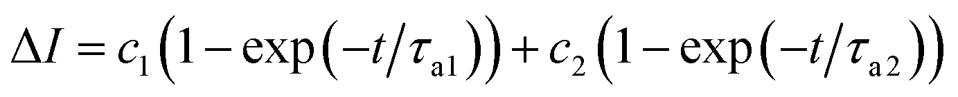 and
and 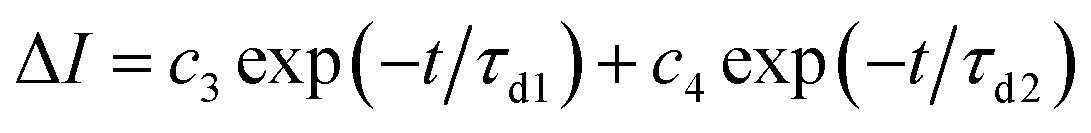 , respectively. Therein, τa1 and τd1 are separately the time constants of fast rise and decay, and τa2 and τd2 are the slow rise and decay. The fitting parameters of these time constants are listed in Table 2. The fast time constant should be associated with the carrier transfer from BP to graphene, and the slow time constant is usually attributed to the charge transport process in the light sensitizers,35,39 which are BP nanosheets, especially the multilayer BP nanosheets in this study. Notice that τd1 and τd2 are larger than τa1 and τa2, respectively. We speculate the reason is that the energy barrier at the interface of BP and graphene hinders the inverted charge transfer, thus slowing down the charge recombination process.