
 Open Access Article
 This Open Access Article is licensed under a
 Creative Commons Attribution 3.0 Unported Licence
Enhancement of the electrical conductivity of defective carbon nanotube sheets for organic hybrid thermoelectrics by deposition of Pd nanoparticles†
Keisuke
Oshima
a,
Yukihide
Shiraishi
 bc,
Takuya
Matsumura
b,
Ayumi
Kuriyama
b,
Kazuki
Taguchi
a,
Junta
Inoue
b,
Hiroaki
Anno
cd and
Naoki
Toshima
*c
bc,
Takuya
Matsumura
b,
Ayumi
Kuriyama
b,
Kazuki
Taguchi
a,
Junta
Inoue
b,
Hiroaki
Anno
cd and
Naoki
Toshima
*c
aGraduate School of Engineering, Sanyo-Onoda City University (formerly Tokyo University of Science Yamaguchi), Sanyo-Onoda, Yamaguchi 756-0884, Japan
bDepartment of Applied Chemistry, Sanyo-Onoda City University (formerly Tokyo University of Science Yamaguchi), Sanyo-Onoda, Yamaguchi 756-0884, Japan
cOrganization for Research Promotion, Sanyo-Onoda City University (formerly Tokyo University of Science Yamaguchi), Sanyo-Onoda, Yamaguchi 756-0884, Japan. E-mail: toshima@rs.tus.ac.jp
dDepartment of Electrical Engineering, Sanyo-Onoda City University (formerly Tokyo University of Science Yamaguchi), Sanyo-Onoda, Yamaguchi 756-0884, Japan
First published on 17th October 2020
Abstract
Although a single carbon nanotube (CNT) has a high thermal conductivity, the randomly assembled sheet has a high potential to be used as an effective thermoelectric (TE) film because of the high electrical conductivity due to the intrinsic property of the CNT and the low thermal conductivity due to phonon scattering at the interfaces of the CNTs. Nevertheless, the high cost of the CNTs limits the practical application of the CNT sheets in TE devices. The recent mass-production of inexpensive CNTs may resolve this problem, although the mass-produced CNTs have many more defects on their surface, which often reduces the electrical conductivity in comparison to the expensive CNTs. We have now discovered that the deposition of palladium nanoparticles (Pd NPs) can enhance the electrical conductivity of the CNT sheets. The electrical conductivity of the mass-produced and defective super-growth CNT (SGCNT) sheets has been found to be increased from about 90 S cm−1 to 170 S cm−1 by depositing the Pd NPs on the SGCNTs by an accumulated chemical reduction method. The results suggested the possibility that the Pd NPs could deposit on the defective sites of the SGCNTs, which produced the improved electrical conductivity of the CNT sheets. Because the SGCNT sheets have a low thermal conductivity, the thermoelectric figure-of-merit (ZT) at room temperature was estimated to be as high as ∼0.3.
Introduction
Single-walled carbon nanotubes (SWCNTs) have received much attention since their first discovery by Iijima et al.1 and Bethune et al.2 in 1993. Many fundamental research studies have been carried out since then, which reported that SWCNTs could be semiconducting or metallic,3,4 have diameter-dependent optical and electrical band gaps,4–6 and have many attractive properties such as incredibly high charge carrier mobilities.7 Although the as-prepared SWCNTs are mixtures, separation and purification techniques have been developed establishing the SWCNTs as a versatile electronic material and providing high-performance applications, such as transistors,8 biological imaging fluorophores,9 photovoltaics,10etc. In the past decade, nanomaterials, especially SWCNTs, have also attracted increasing attention as organic and/or hybrid thermoelectric (TE) materials, too,11–19 which are essential for developing TE devices for harvesting electrical energy from low-grade waste heat20 as well as for the so-called “IoT.”21 Although a single CNT has a high thermal conductivity, a randomly assembled CNT sheet or network has a much lower thermal conductivity than that of the single CNT due to phonon scattering at the interfaces of the CNTs in the CNT sheets, but maintains a high electrical conductivity.22 Thus, the CNT sheets have a significant potential to be used in TE devices.There have been many reports about the electronical conductivity and Seebeck coefficient of the sheets of various SWCNTs.15 The electrical conductivity and Seebeck coefficient of the SWCNT depend on its diameter, chirality, and doping.13,15 Thus, separation and purification are necessary to obtain the CNT with a high TE performance. In fact, a CNT sheet with a high Seebeck coefficient was reported to have a high TE performance.23,24 In addition, the composites of the CNTs with electric conducting or insulating polymers showed a higher performance as practically processable TE materials.25,26 We have proposed a ternary hybrid TE material composed of CNTs, a nano-dispersed polymerized nickel complex (poly(nickel 1,1,2,2-ethylenetetrathiolate), PETT)27 and poly(vinyl chloride) with a high TE performance.28 Grunlan and Yu's group reported that a 40-quadlayered polyelectrolyte carbon nanocomposite prepared by the layer-by-layer deposition of polyaniline/graphene/polyaniline/double-walled CNT showed an extremely high maximum power factor.29 These reports have clearly shown that CNTs are promising materials for TEs.
As already mentioned, however, the CNTs, which were effective for a high TE performance, were usually the specialized CNTs and very expensive. Recently, inexpensive CNTs were mass-produced in a factory by a super-growth (SG) method.30 However, the disadvantage of the SGCNT is the presence of many defects on a tube, which results in a low electrical conductivity. We wanted to improve the electrical conductivity of the defective SGCNTs, because the electrical conductivity is a key factor to enhance the TE performance, i.e., the TE figure-of-merit (ZT).
Hybridization is one of the popular techniques to improve the physical property of materials, and often prefer nanomaterials as the component. In fact, there are many reports about hybrids of one-dimensional nanomaterials like CNTs or conducting polymers with metal NPs to improve the physical property of the nanomaterials.14,15,31–40 Among them, however, only a few reports were concerned with the hybrid thermoelectric materials composed of SWCNTs and metal NPs.36–40 In 2011, C. Yu et al.36 reported the decoration of arc-discharged SWCNTs with Au NPs by the reaction with HAuCl4. The gold reduction allow electron withdrawal from the CNTs, resulting in a 1.5 times higher conductance, but half the thermopower on the produced composites. Thus, the thermoelectric power factor (PF = σS2, where σ and S denote electrical conductivity and thermopower (Seebeck coefficient), respectively), which is a factor denoting the thermoelectric performance, was unfortunately 0.375 times the value of the pristine CNT. His group37 also showed the thermoelectric properties of the composite composed of Au NP/SWCNT (by a HipCo method)/PEDOT-PSS (poly(3,4-ethylenedioxythiophene))-poly(styrene sulfonate)/PVAc (poly(vinyl acetate)) (15/60/15/10 in wt%). It had a high electrical conductivity (∼6000 S cm−1), 6 times higher than that of the pristine composite without Au NPs (SWCNT/PEDOT-PSS/PVAc: 60/30/10 in wt%), but again a lower Seebeck coefficient (11 μV K−1), which was 0.275 times the value of the pristine one, resulting in a 0.453 times the power factor value of the pristine one. Thus, the galvanic method could be insufficient for improvement of the TE performance by decoration of the CNT with metal NPs. In 2013, Fernandes et al.38 prepared composites of Au NP/CNT by a mixture of Au NPs (5 and 60 nm in average diameter) and SWCNTs dispersed by 1 wt% of a surfactant, sodium dodecyl sulfate, in water. The addition of small and large Au NPs decreased the electrical conductivity from 1800 S cm−1 for the pristine CNT to 620 and 790 S cm−1 for the composite of the small and large Au NPs, respectively, and also decreased the Seebeck coefficient from 31 μV K−1 to ∼25 μV K−1, resulting in a decreased power factor from 167 μW m−1 K−2 to 420 and 470 μW m−1 K−2 for the small and large Au NPs, respectively. In this case, therefore, no improvement was observed by incorporation of the Au NPs. In 2016, An et al.39 succeeded in covering the porous CNT webs with Au NPs by reduction of AuCl3 with the CNTs. The coverage increased the electrical conductivity from 1000 S cm−1 for the pristine CNT web to 5000 S cm−1, and decreased the Seebeck coefficient from ∼120 μV K−1 to ∼80 μV K−1, resulting in an improvement of the power factor from ∼1500 μW m−1 K−2 to ∼3500 μW m−1 K−2 and a more than 2-fold improvement in the TE figure-of-merit ZT from 0.079 to 0.163. After covering, polyaniline (PANi) was integrated into the Au-doped CNT webs leading to an electrical conductivity of ∼1000 S cm−1, Seebeck coefficient of ∼150 μV K−1, power factor of ∼2200 μW m−1 K−2, and ZT of 0.203, which is one of the highest ZT values reported for organic TE materials. In 2017, we prepared CNT-based hybrid films by the physical mixture of SWCNTs and Pd NPs (2.2 and 6.2 nm average diameters) with and without poly(vinyl chloride) (PVC) (4![[thin space (1/6-em)]](https://www.rsc.org/images/entities/char_2009.gif) :0.4:6 and 10:1:0 in wt ratio, respectively) in NMP (N-methylpyrrolidone).40 In the resulting hybrid films containing PVC, the addition of the larger Pd NPs (commercially-available Pd black) slightly decreased the electrical conductivity with almost no change in the Seebeck coefficient, while the addition of the smaller Pd NPs (prepared separately by ourselves) significantly improved the electrical conductivity from ∼67 S cm−1 to ∼95 S cm−1 (about 1.4 times higher) and slightly increased the Seebeck coefficient. For the hybrids of the CNTs and Pd NPs without PVC, the electrical conductivity was increased from 52 S cm−1 to 93 S cm−1 by incorporation with the small Pd NPs, while the Seebeck coefficient remained nearly constant with a slight increase (from 52.4 μV K−1 to 58.7 μV K−1). These previously published metal NP-containing SWCNT-based hybrids can be classified into two types, i.e., those produced by the accompanying reaction withdrawing electrons from the CNTs (ref. 36, 37 and 39) and those produced without such a reaction (ref. 38 and 40). In the former case, the reaction provided holes (carriers) to the CNTs, resulting in a significant improvement in the electrical conductivity, but a decrease in the Seebeck coefficient by the incorporation of metal NPs. In the latter case, on the other hand, the electrical conductivity decreased if the NPs were large, and moderately increased if the NPs were sufficiently small. As for the Seebeck coefficient, large NPs decreased it, but, if the NPs were small, it remained nearly constant. In addition, it is noteworthy that the metal NPs were randomly deposited on the surface of the CNTs in these hybrids.
:0.4:6 and 10:1:0 in wt ratio, respectively) in NMP (N-methylpyrrolidone).40 In the resulting hybrid films containing PVC, the addition of the larger Pd NPs (commercially-available Pd black) slightly decreased the electrical conductivity with almost no change in the Seebeck coefficient, while the addition of the smaller Pd NPs (prepared separately by ourselves) significantly improved the electrical conductivity from ∼67 S cm−1 to ∼95 S cm−1 (about 1.4 times higher) and slightly increased the Seebeck coefficient. For the hybrids of the CNTs and Pd NPs without PVC, the electrical conductivity was increased from 52 S cm−1 to 93 S cm−1 by incorporation with the small Pd NPs, while the Seebeck coefficient remained nearly constant with a slight increase (from 52.4 μV K−1 to 58.7 μV K−1). These previously published metal NP-containing SWCNT-based hybrids can be classified into two types, i.e., those produced by the accompanying reaction withdrawing electrons from the CNTs (ref. 36, 37 and 39) and those produced without such a reaction (ref. 38 and 40). In the former case, the reaction provided holes (carriers) to the CNTs, resulting in a significant improvement in the electrical conductivity, but a decrease in the Seebeck coefficient by the incorporation of metal NPs. In the latter case, on the other hand, the electrical conductivity decreased if the NPs were large, and moderately increased if the NPs were sufficiently small. As for the Seebeck coefficient, large NPs decreased it, but, if the NPs were small, it remained nearly constant. In addition, it is noteworthy that the metal NPs were randomly deposited on the surface of the CNTs in these hybrids.
We have now designed a new type of hybrid film by making metal NPs mainly deposited on the defect sites on the surface of the CNTs. For this purpose, the defective SGCNTs are a favorite material for the hybrids, because the defects are considered to be holes or vacancies which may be functionalized with polar groups like the COOH group. Thus, we have tried various methods for the hybridization of the SGCNTs with palladium nanoparticles (Pd NPs), and discovered that the chemical deposition of Pd NPs on the SGCNTs can enhance the electrical conductivity of the CNT sheets, resulting in an improved ZT value (ZT ∼ 0.3) by the hybridization. This ZT value is one of the highest ZT values reported for organic TE materials.14,15,28 These results suggested the possibility that the Pd NPs could cover the defective sites of the SGCNTs, in other words, repair the defects of the SGCNTs. This can provide a new concept to the chemistry and physics of CNTs.
Experimental
Materials
Palladium black (purity: 99.95%) and palladium acetate were purchased from Kojima Chemical Co., Ltd, Japan. 1-Methyl-2-pyrrolidone (NMP, for peptide synthesis), hydrochloric acid (reagent grade), nitric acid (for analysis of poisonous metals), and methanol (reagent grade) were obtained from the FUJIFILM Wako Pure Chemical Corporation. The super-growth carbon nanotube (SGCNT) was kindly provided by the Nippon ZEON Corporation, Japan. The provided SGCNTs were SWCNTs with a diameter of about 3–8 nm and a length of about 1–100 μm.Preparation of free Pd NPs by a chemical reduction method
The reduction of palladium ions was carried out by heat treatment of a NMP solution of palladium acetate (1.4 mmol L−1) in a flask placed in an oil bath at 100 °C for 45 min. Quick cooling of the reaction solution in the flask with iced water resulted in the formation of a dispersion of the free Pd NPs.Preparation of sheets of SGCNTs decorated by Pd NPs by a physical mixture
The SGCNTs were dispersed in NMP using a jet mill at the concentration of 2.0 mg mL−1. The Pd NP dispersion in NMP (0.15 mg mL−1), separately prepared by a chemical reduction method or by a mixture with commercially-available Pd black, was mixed with the above-prepared SGCNT dispersion in NMP at the weight ratio of Pd:CNT = 1:9, 2:8, 3:7, and 5:5 by using a magnetic stirrer for 30 min. The suction filtration of the mixed dispersion on a membrane filter provided the wet sheets, which were washed with methanol several times, well dried at room temperature in air, then completely dried under vacuum at 40 °C overnight to produce dry sheets.
Preparation of Pd NP-decorated SGCNTs by an accumulated chemical reduction method
The SGCNT dispersion in NMP prepared using a jet mill at the concentration of 2.0 mg mL−1 was mixed with a palladium(II) acetate solution in NMP (1.4 mmol L−1). The mixed dispersion was heated in an oil bath at 100 °C for 45 min while stirring, resulting in a Pd NP-decorated SGCNT dispersion (abbreviated as Pd@SGCNT). The sheets were prepared from the dispersions by the same method as the dispersions prepared using a physical mixture.Measurement and instruments
All the measurements were carried out at least more than three times, and the average value is shown as the result of all the experiments.000. The average diameter was obtained for 200 particles.
Raman spectrum. Raman spectra were obtained using an NRS-7100 Laser Raman spectrometer (JASCO, Japan) with a 532 nm green line laser.
Results and discussion
Preparation of the hybrids of SGCNTs with Pd NPs
We previously reported the thermoelectric hybrid films of the SGCNTs and Pd NPs with poly(vinyl chloride) (PVC).40 We initially tried the hybridization of the SGCNTs with Pd NPs by a physical mixture. Palladium black (commercially-available Pd NPs, average diameter dav = 3.5 ± 1.2 nm, Fig. S1a, ESI†) and a dispersion of Pd NPs separately prepared by a chemical method (dav = 2.7 ± 0.9 nm, Fig. S1b, ESI†) were used for this purpose. The scanning electron microscopy (SEM) images of the sheets prepared from the SGCNTs covered by the Pd black and separately-prepared Pd NPs (Fig. S2b and c, ESI,† respectively) suggested that the Pd black NPs were aggregated on the surface of the SGCNTs, while the separately prepared Pd NPs were more separately and homogeneously deposited on the SGCNTs than the Pd black NPs. The TE properties (Seebeck coefficient (S), electrical conductivity (σ), and TE power factor (PF = S2σ)) for the SGCNT sheets covered with Pd black and separately-prepared Pd NPs were measured. No improvement in the TE properties was observed for the SGCNT sheets covered with the Pd black (Fig. S3, ESI†), while the hybrids with the separately-prepared Pd NPs provided a slight improvement in the electrical conductivity and power factor of the sheets as shown in Fig. 1. These results suggest that the separately-prepared Pd NPs, which are smaller in size and more mono-dispersed than the Pd black, can more easily form the hybrids with the SGCNTs than Pd black, probably because the smaller Pd NPs can cover the defect sites on the surface of the SGCNTs by smooth interaction with the functional groups near the defects.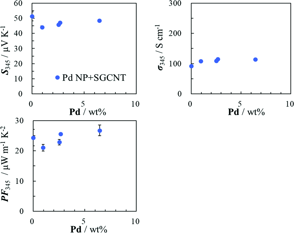 | ||
| Fig. 1 Palladium content dependence of the Seebeck coefficient (S), electrical conductivity (σ) and power factor (PF = S2σ) of the sheet of SGCNTs covered with the separately-prepared palladium NPs at 345 K. | ||
The appropriate hybridization of the SGCNTs with Pd NPs may require the deposition of sufficiently small Pd NPs on the exact defective sites of the SGCNTs. For this purpose, we have developed an accumulated chemical reduction method based on our long and extensive experience regarding the preparation of metal nanoparticles. The idea has been conceived based on the properties and formation mechanism of dispersion of the metal NPs in presence of functional polymers in solution.41–43 By this method, we expected to succeed in the appropriate hybridization of the SGCNTs with Pd NPs. An NMP (N-methyl-2-pyrrolidone) solution of Pd(II) acetate was mixed at room temperature with a dispersion of SGCNTs in NMP, resulting in the possible adsorption of Pd ions on the defects because the defects were supposed to be active sites having functional groups. The mixed dispersion in NMP was treated by heat, resulting in reduction of the adsorbed Pd ions by NMP as a reductant to form Pd atoms or clusters at the defects of the SGCNTs. A continuous heat treatment of the dispersion was expected to cause the accumulative deposition of Pd atoms to form the Pd NPs at the defect sites of the SGCNTs. In this case, the functional groups at the defects on the SGCNTs were predicted to play a protectant role to stabilize the small Pd NPs. The hybrids composed of the Pd NPs and SGCNTs (Pd@SGCNT) were observed by transmission electron microscopy (TEM). The TEM image of the Pd@SGCNT (Fig. 2a) suggests the presence of Pd NPs on the CNTs, and the average diameter of the Pd NPs was found to be 2.9 ± 1.1 nm (Fig. 2b). A high-resolution TEM (HRTEM) image (Fig. 2c) might show the deposition of a Pd NP at a rather defective site on the surface of the CNT. The deposition of Pd NPs at the defects of a CNT is schematically illustrated in Fig. 2d. The NP-decorated CNT can be called a “Marshal's baton” (Fig. S4, ESI†), where the baton is covered by metal ornaments. As for the location of the Pd NPs at the defect sites on the SGCNTs, there is no direct evidence at the present time. However, we have much supporting evidence for the location, which is discussed in a later section. Based on these facts, we postulated that the Pd NPs produced by the chemical method in the presence of the SGCNTs can mainly deposit at the defect sites on the SGCNTs.
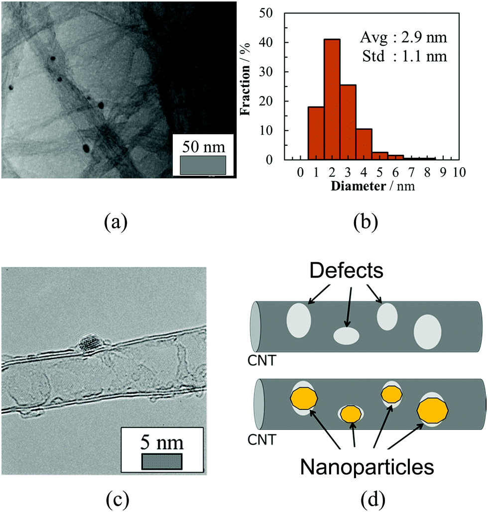 | ||
| Fig. 2 (a) TEM image of Pd@SGCNT (Pd content = 9.47 wt%), (b) size distribution histogram of Pd NPs in Pd@SGCNT (Pd content = 9.47 wt%), (cf. Fig. S10, ESI,† in which not the “fraction” but the “count” is used as the ordinate), (c) HRTEM micrograph of Pd@SGCNT (Pd content = 11.0 wt%), and (d) schematic illustration of defective CNT and NP-covered CNT. | ||
There are reports about the supported metal NPs on the surface of carbon nanomaterials like CNTs and graphenes.44–48 However, only a few reports described the applications of the supported metal NPs on the SWCNTs for the hybrid thermoelectric materials.36–40 The support of metal NPs on CNTs generally requires chemical modification of the CNTs on the surface or at the edge. For example, the oxidation of the CNTs by a strong acid can introduce functional groups like –OH and –COOH,49 which can interact with the metal NPs. However, the oxidation usually damages the CNTs and decreases the electrical conductivity. Utilization of a surfactant or polymer binder can provide another method to introduce metal NPs on the surface of the CNTs. Fujigaya and Nakashima reported hybrid materials supporting platinum NPs using poly(benzoimidazole).50 In this case, the NPs were well dispersed, but no enhancement in the electrical conductivity was observed. In contrast, our method is very mild and does not require the use of extra additives, and thus expected to readily cover the defects with NPs and enhance the electrical conductivity of the defective CNTs, as described in a later section.
Characterization of the hybrids of the SGCNTs with Pd NPs
In order to characterize the hybrids of the SGCNTs and Pd NPs, we used Raman spectroscopy and X-ray photoelectron spectroscopy (XPS) in addition to the TEM described in the previous section. Raman spectroscopy is a useful method to characterize the crystallinity of the CNTs. The peaks at about 1600 cm−1 (G-band) and 1350 cm−1 (D-band) are attributed to sp2 carbons with a 6-membered graphene skeleton and sp3 carbons with an amorphous structure, respectively.51,52 The intensity ratios of the G- and D-band (G/D ratio) were usually over 10 for the pure single-walled CNTs like those prepared by the MEIJO eDIPS, HiPco, and laser methods, while the G/D ratio of the SGCNTs was as low as 1.5 (Fig. S5, ESI†), because they had many defective sites. However, the G/D ratio of the Pd NP-covered SGCNTs (Pd@SGCNT) was found to be 2.5 (Fig. S5, ESI†), which was slightly higher than that of the free SGCNTs. This increase in the G/D ratio might be considered as the results of the coverage of the defects of the SGCNTs by the Pd NPs.X-Ray photoelectron spectroscopy (XPS) is a useful measurement technique which shows not only what elements are present within a film but also what other elements they are bonded to. We measured the XPS spectra of the sheet of the blank SGCNTs (sample 1) and those of the Pd NP-covered SGCNTs (Pd@SGCNT) with various Pd contents (samples 2, 3, and 4 with 4.62, 9.47, and 17.43 wt% Pd contents, respectively). The results are summarized in Table 1 and the original XPS spectra are shown in Fig. S6 and S7 (ESI†). The Pd concentration of the Pd@SGCNT in Table 1 is reasonably increased with the increased content of Pd. The metallic Pd rather than ionic Pd is increased with the increased Pd content. This is also acceptable because the size of the Pd NPs in Pd@SGCNTs is increased with the increased Pd content, and the smaller Pd NPs contain more ionic Pd due to easy oxidation of the surface atoms in the Pd NPs. In addition, the ionic Pd could be attributed to the surface Pd atoms coordinated to oxygen atoms. Another important aspect in Table 1 is that the content of the functionalized carbons with the COO, C![[double bond, length as m-dash]](https://www.rsc.org/images/entities/char_e001.gif) O, C–O, and C–H/C–C structures is increased from 19.2 wt% to 26.6 wt% with the increase in the Pd content, which suggests that the Pd NPs are supported at the active sites with the functionalized carbons through the chemical bond of C–O–Pd.
O, C–O, and C–H/C–C structures is increased from 19.2 wt% to 26.6 wt% with the increase in the Pd content, which suggests that the Pd NPs are supported at the active sites with the functionalized carbons through the chemical bond of C–O–Pd.
| Sample | C | O | Pd | |||||||
|---|---|---|---|---|---|---|---|---|---|---|
| COO | CO |
C–O | C–H/C–C | Carbon | O–H/O–C | OC |
Pd(IV) | Pd(II) | Pd(metal) | |
| 1 | Total C: 97.0 | Total O: 2.1 | ||||||||
| 0.9 | 1.2 | 1.6 | 15.6 | 77.8 | 1.3 | 0.8 | ||||
| 2 | Total C: 93.8 | Total O: 1.6 | Total Pd: 0.4 | |||||||
| 0.8 | 1.6 | 2.4 | 15.1 | 74.0 | 0.7 | 0.9 | 0.3 | <0.1 | 0.1 | |
| 3 | Total C: 94.4 | Total O: 1.8 | Total Pd: 0.7 | |||||||
| 0.9 | 1.5 | 2.2 | 17.8 | 72.1 | 0.8 | 1.1 | 0.3 | 0.1 | 0.3 | |
| 4 | Total C: 92.1 | Total O: 2.7 | Total Pd: 1.3 | |||||||
| 1.0 | 1.5 | 2.1 | 22.1 | 65.5 | 1.0 | 1.7 | 0.5 | 0.1 | 0.7 | |
Thermoelectric properties of the chemically hybridized SGCNT sheets
The TE properties of the sheet of SGCNTs covered by the Pd NPs using the accumulated chemical reduction method (Pd@SGCNT) were measured at 345 K. The Pd content dependence is shown in Fig. 3. In order to compare the change in the electrical conductivity at the same weight percentage of the Pd NPs on the SGCNTs with the chemical method and physical ones, we have tried to obtain approximate expressions by the secondary curves for the relation between the Pd content (wt%) and electrical conductivity from the experimental results in the systems of Pd black + SGCNT, Pd NP + SGCNT, and Pd@SGCNT, respectively, which are shown as Fig. S8 (ESI†). From these curves, we estimated the electrical conductivity of three types of Pd-covered SGCNT sheets at the Pd contents of 6, 8, 10, and 12 wt%, respectively, which are shown in Table S1 (ESI†). From the data in this table, the improvement in the electrical conductivity of the SGCNT sheet by decoration with 14 wt% of the Pd NPs by the chemical reduction is as large as 69.0%, while the improvements are as small as 8.1% for the SGCNT sheet with the Pd black by the physical mixture. It is noteworthy that only the decoration with Pd NPs by the chemical reduction method can effectively improve the electrical conductivity of the SGCNT sheet. At the maximum Pd content (17.4 wt%), the Seebeck coefficient (S) and electrical conductivity (σ) of the sheet of the Pd@SGCNT hybrid were ∼56 μV K−1 and ∼160 S cm−1, respectively, resulting in the power factor (PF) of ∼52 μW m−1 K−2. This value is about twice that of the blank sheet of the SGCNTs without the Pd NPs. The maximum Pd content of the covered SGCNTs (Pd@SGCNT) was higher than that prepared by the physical mixture with separately-prepared Pd NPs. This result predicts a stronger interaction of the Pd NPs with SGCNT in the chemically covered SGCNTs (Pd@SGCNT) than that in the physically covered ones. The strong interaction may cause a much higher electrical conductivity and power factor of the former sheet than the latter one. This strong interaction can suggest the presence of a type of the charge transfer interaction between the NPs and CNT, which might provide the enhancement in the electrical conductivity of the CNT sheets, as described in the next paragraph.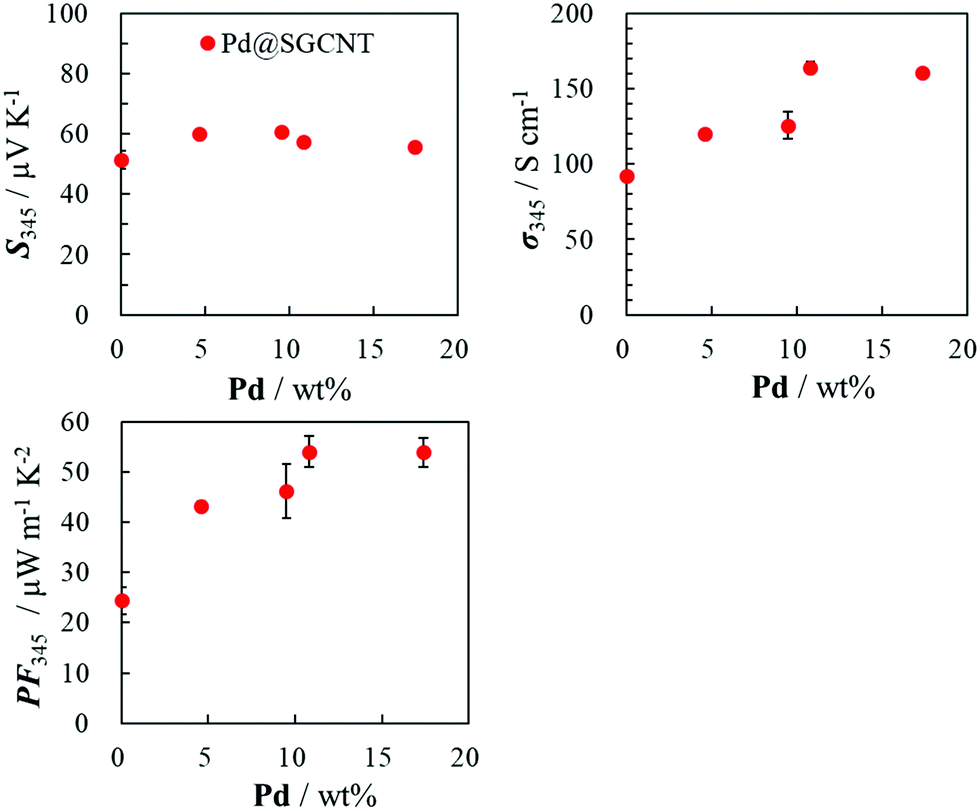 | ||
| Fig. 3 Palladium content dependence of the Seebeck coefficient (S), electrical conductivity (σ) and power factor (PF = S2σ) of the sheet of SGCNTs covered with palladium NPs by the accumulated chemical reduction method at 345 K. | ||
In order to clarify the effect of the Pd NPs on the increase in the electrical conductivity of the SGCNT sheets, the electrical conductivity (σ), carrier concentration (n), and carrier mobility (μ) of the Pd NP-covered SGCNTs and blank SGCNTs were determined based on a Hall measurement by the van der Pauw method, with the relation of σ = enμ (e: elementary charge). The results are listed in Table 2. The covering by the Pd NPs does not affect the carrier concentration but leads to the increased carrier mobility. This result suggests that the Pd NPs could cover the defects of the SGCNTs, which results in the increased carrier mobility. In other words, the metal NPs might interact strongly with SGCNTs by a kind of charge transfer interaction to form a weak bond, i.e., the NPs might repair the defects of the SGCNTs, which could not increase the carrier concentration, but provide a smooth motion of the carriers on the surface of the SGCNTs. This increased carrier mobility could be considered to be due to the covering effect of the Pd NPs rather than the change in the structure or morphology of the surface of the CNT sheets due to the lack of difference in the magnified SEM photographs (Fig. S9, ESI†). In contrast, the nearly constant or slightly decreased carrier concentration can result in the nearly constant or slightly increased Seebeck coefficient S because the Seebeck coefficient is a function of the carrier concentration n in the relation of S = (8π2kB2m*T/3qh2)(π/3n)2/3 where kB, h, m*, T, and n denote the Boltzmann constant (1.38 × 10⁻²³ J K−1), Planck constant (6.63 × 10⁻³⁴ J s), effective mass of the carrier, absolute temperature, and carrier concentration, respectively, and q = ±e. This speculative consideration is very consistent with the experimental results.
| σ/S cm−1 | n/cm−3 | μ/cm2 (V s)−1 | |
|---|---|---|---|
| Blank | 94.6 | 3.2 × 10²⁰ | 2.0 |
| Pd@SGCNT | 207 | 2.4 × 10²⁰ | 5.5 |
TE performance of the hybrid SGCNT sheets
The TE performance of the materials can be evaluated by the TE figure-of-merit ZT, which can be calculated by the equation, ZT = (S2σ/κ)T, where S, σ, κ, and T denote the Seebeck coefficient, electrical conductivity, thermal conductivity and absolute temperature, respectively. It is well known that there is an anisotropy in the electrical and thermal conductivities of the CNT sheets. Inoue et al. reported that both the electrical and thermal conductivities of the sheets composed of multi-walled CNTs in an in-plane direction are about 8 times higher than those in the through-plane direction.53 Since we could not measure the thermal conductivity of the CNT sheets in the in-plane direction at present, we estimated that the thermal conductivities of our samples in the in-plane direction might be 8 times higher than those in the through-plane direction.The thermal conductivities of the pristine and Pd NP-deposited SGCNT sheets measured in the through-plane direction are shown in Table S2 (ESI†). The thermal conductivities of the pristine SGCNT sheet and Pd@SGCNT sheet in the in-plane direction were estimated to be 0.4 W m−1 K−1 and 0.64 W m−1 K−1, respectively, which were used for the calculation of the ZT value. In order to understand the low thermal conductivity of the SGCNT sheets with and without the Pd NPs, it is noteworthy to provide the following discussion. Generally, the thermal conductivity κ is the sum of the phonon component κph and carrier component κe (κ = κph + κe). In addition, the carrier component can be calculated from the electrical conductivity according to the Wiedemann–Franz law shown in the equation κe = LσT, where L and T denote the Lorentz number (2.44 × 10⁻⁸ W Ω K−2) and absolute temperature, respectively. The calculated carrier components of the thermal conductivity (κe) in the in-plane direction of the pristine SGCNT sheet and Pd@SGCNT with the highest electrical conductivity in the through-plane direction were 0.07 W m−1 K−1 and 0.15 W m−1 K−1, respectively. The typical CNT sheet has a high electrical conductivity, which leads to the high thermal conductivity. However, the SGCNTs are very porous with many defects, and have a rather larger diameter (3–8 nm) with a longer length (about 100 μm) than the typical CNTs. The many defects and large diameter provide a low electrical conductivity (50–300 S cm−1) and thus, a low thermal conductivity. In addition, our SGCNT sheets are as thick as approximately 20 μm, which may allow random alignment of the SGCNTs in the sheet, resulting in the low density and rather low conductivity. Thus, we consider that the low thermal conductivity of the SGCNT sheet and Pd NP-decorated SGCNT ones could be attributed to the physical properties of the SGCNT, i.e., the high porosity and high surface area with many defects, and the low density of the SGCNT sheet because of the rather low alignment of the SGCNTs in the sheet.
The calculated ZT values based on this estimation are summarized in Fig. 4. The blank sheet composed of only the SGCNTs is estimated to have the ZT value of 0.14 at 345 K, and the sheet of Pd@SGCNT with 9.5 wt% Pd has the highest value of 0.30 at 345 K, which is 2.1 times higher than that of the blank one. Nakai et al. reported the ZT value of 0.33 at 340 K for the sheet composed of the selected single-walled CNTs with a high Seebeck coefficient, which were collected by extraction and purification.23 We have succeeded in simply obtaining sheets with a similar high ZT value by chemical coverage of the inexpensive SGCNTs with Pd NPs. The pristine SGCNT sheets have a low electrical conductivity due to their many defects. We approached this problem from a different angle and regarded them not as defective sites but as active sites. This revolutionary idea provided the effect of Pd NPs to repair the SGCNT defects. The effects of metal NPs on the electrical conductivity of organic TE compounds have been reported. In the hybrid materials of conducting polyaniline doped with a small amount of gold or platinum NPs, for example, the electrical conductivity was slightly improved by the doping.33 In the conducting poly(3,4-ethylenedioxythiophene)-poly(styrenesulphonate) (PEDOT-PSS), the addition of a small amount (e.g., 0.01 wt%) of poly(N-vinyl-2-pyrrolidone) (PVP)-protected gold or silver NPs provide the increased electrical conductivity, and thus, the power factor of the films.54–56 The increase in the electrical conductivity and power factor could be accelerated by altering the type of protectant and metal in the hybrid PEDOT-PSS TE films.57 The effect of metal NPs has been explained by a bridging effect of the NPs between the conducting polymers with NPs, but the complete mechanism has not yet been clarified. There are also a few reports about the improvement of the TE properties of the SWCNTs by the addition of metal NPs.36–40 The authors claim the effect of bridging nanotubes and the modification of the Fermi level by electron exchange. Such effects of the NPs could be also applied to our case, but the simple concept of the repair of defects by covering the defective sites with NPs might be rather useful to simply understand the present effect.
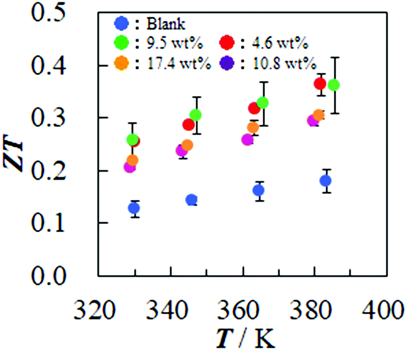 | ||
| Fig. 4 Temperature dependence of the thermoelectric figure-of-merit (ZT) of the sheets composed of SGCNTs only (blank) and Pd NP-covered SGCNTs (Pd@SGCNT) with various Pd contents. Cf. Fig. S11 (ESI†), in which the same data with the more clear error-bars are illustrated. | ||
Discussion about location of the Pd NPs at the defects on the SGCNTs
It is one of the important conclusions in this study that the in situ synthesized Pd NPs are located at the defect sites on the SGCNTs. However, there is no direct evidence for the location of the Pd NPs. Nevertheless, we have many results supporting the location of the Pd NPs in the defect sites.First, the defect sites are modified by functional groups like OH and/or COOH. This is a common idea for the CNTs. In fact, CNTs can be chemically modified by placing these functional groups in the defect sites and at the edges of the CNTs. Second, the polymer-supported Pd NPs are generally prepared by starting from the coordination of Pd ions on the functional groups of the polymers, followed by reduction of the Pd ions to produce Pd atoms, then the Pd clusters (Pd NPs). The coordination of Pd ions to nonbonding electrons of the heteroatoms like O and N in the functional groups is well known in coordination chemistry. Note that the reduction of Pd ions to Pd atoms can be carried out not by the functional groups, but by the solvent, NMP, in the present case. This process for the formation of polymer-supported Pd NPs has been already determined, for example, by the peak shift of the IR spectra.58 By taking account of the first result, the presence of the functional groups at the defect sites, and the second result, formation of Pd NPs at the functional groups, together, we came to the conclusion that the Pd NPs should be located at the sites of the functional groups, i.e., at the defect sites. Third, the TEM photograph might prove the location of the Pd NPs at the defect sites on the CNTs, if the defect site could be clearly detected by TEM. Unfortunately, the defect sites cannot be observed by the TEM in our case. However, the TEM photograph (Fig. 2c) shows the location of the Pd NP on the step site between the double-walled part and single-walled part of the SGCNT. Because the step of the CNTs can be considered to have the functionalized structure, which is similar to the defect sites on the CNTs, the TEM photograph may give evidence supporting the location of the Pd NPs on the defect sites. Fourth, the fact that the chemical reduction method gave a better-dispersed location of the smaller Pd NPs on the SGCNTs in comparison to the physical mixture methods. This was indicated by the SEM (Fig. S2 and S9, ESI†) and TEM photographs (not shown here). In other words, we used the same feeding weight ratio of Pd ions or Pd NPs to the SGCNTs in the three methods. However, the average diameters of the deposited NPs were 2.9 nm, 2.7 nm, and 3.5 nm in the case of the chemical reduction, physical mixture with the separately-prepared Pd NPs, and physical mixture with the commercial Pd black, respectively. This difference in the size of the Pd NPs suggests that the chemical reduction provides the mild conditions for the Pd NP formation, which is attributed to the stabilization of the Pd NPs by functional groups at the defect sites on the SGCNTs. Fifth, for comparison, the same chemical reduction method was applied to the CNTs having different amounts of defective sites, i.e., the reaction was carried out under the same conditions using the SGCNT having many defect sites and a mostly defect-free eDIPS-CNT (MEIJO CNTs prepared by an enhanced Direct Injection Pyrolytic Synthesis method, G/D ratio = 40). The results were quite different for each other. When 50 wt% of Pd ions was supplied to the dispersed SGCNTs, 17.4 wt% of Pd NPs was deposited on the SGCNTs. In contrast, when the same amount of Pd ions was supplied to the eDIPS–CNTs, only 7.8 wt% of Pd NPs was deposited on the eDIPS–CNTs. It is postulated that this difference may be attributed to the facts that the eDIPS–CNTs have fewer defects than the SGCNTs and that the Pd NPs were easily deposited on the defect sites of the CNTs.
Based on these results, we believe that the Pd NPs produced by the chemical method in the presence of the SGCNTs can mainly deposit at the defect sites of the SGCNTs.
Discussion about a possible mechanism of the improved electrical conductivity for the Pd NP-deposited SGCNT sheets
There are many reports about the enhancement of the electrical conductivity of CNT sheets.13–15 Most of them claimed that the increased electrical conductivity was realized by doping the CNTs with an acid or base as a dopant. In their methods, the carrier concentration was raised by the doping.However, there are only a few reports about the improved TE performance of CNT sheets decorated by metal NPs. Yu et al.36 prepared the Au NP-decorated SWCNT films by galvanic displacement, in which the diameters of the Au NPs were a few tens of nanometers. The Au NPs on the CNTs decreased the electrical conductivity, but the Seebeck coefficient increased, resulting in a 2-fold increase in the TE power factor. Upon the NP precipitation, electron transfer occurred in order to equilibrate the Fermi levels of the materials in contact. Thus, the Au NP decoration made the CNTs more p-type by withdrawing electrons from the CNTs. Additionally, tube–tube junctions may have been modified as a result of bridging the nanotubes with the NPs. The same group32–37 also reported TE composite films of Au NP/SWCNT(HipCo)/PVAc(600BP)/PEDOT:PSS (15:60:10:15 in vol%), where the electrical conductivity was as high as ∼6000 S cm−1 while the Seebeck coefficient was ∼13 μV K−1. The authors claimed that the high conductivity could be due to p-type doping caused by the Au NPs when they were precipitated on the CNTs. They also claimed that a CNT dispersion with a proper amount of CNT dispersants was crucial to maximize the electrical conductivity. Fernandes et al.38 found that the incorporation of the Au NPs deteriorated the TE properties of the CNT films, which was sensitive to the size of the used Au NPs. Thus, the addition of small (∼5 nm in diameter) Au NPs to the CNTs made the electrical conductivity, Seebeck coefficient, and thermal conductivity decrease from 1800 S cm−1 to 620 S cm−1, from 31 μV K−1 to ∼25 μV K−1, and from 82 W m−1 K−1 to 73 W m−1 K−1, respectively. The power factor and the TE figure of merit (ZT) also decreased from 1.67 × 10⁻⁴ W m−1 K−2 to 4.2 × 10⁻⁵ W m−1 K−2 and from 6.04 × 10⁻⁴ to 1.73 × 10⁻⁴, respectively. In this case, the Au NPs were just contaminants. An et al.39 reported the CNT bundles, which were interconnected by a direct spinning method to form 3D networks without interfacial contact resistance, provided both a high electrical conductivity and high carrier mobility. Covering the porous CNT webs with Au NPs increased the electrical conductivity, resulting in the optimal ZT of 0.163, which represented a more than 2-fold improvement compared to the ZT of the pristine CNT webs (0.079). In this case, the authors claimed that the Au NPs improved the carrier mobility. After coverage, polyaniline (PANI) was integrated into the Au-doped CNT webs to both improve the Seebeck coefficient by an energy-filtering effect and decrease the thermal conductivity by the phonon-scattering effect. This led to a ZT of 0.203. Previously, we prepared hybrid TE films only by mixing the CNTs, PVC, and separately-prepared Pd NPs.40 The TE properties were slightly improved by the Pd NPs in the three-component films, in which the Pd NPs were used for promotion of the carrier transport between the CNTs and poly(vinyl chloride) (PVC), as a binder of the CNTs.
In contrast, it is clear in our present method that the chemical deposition of the Pd NPs on the defective SGCNTs clearly improved the carrier mobility of the CNTs based on the Hall measurement. Thus, the increase in the electrical conductivity of the SGCNT sheets by the deposition of Pd NPs may not be attributed to the normal doping effect. It could be considered that the metal NPs might strongly interact with the SGCNTs by a kind of charge transfer interaction to form a weak bond, i.e., the NPs might repair the defects of the SGCNTs, which could not increase the carrier concentration, but provide a smooth motion of the carriers on the surface of the SGCNTs. This increase in the carrier mobility could be attributed to the covering effect of the Pd NPs rather than the change in the structure or morphology of the surface of the CNT sheets because no difference was clearly observed in the magnified SEM photographs (Fig. S2 and S9, ESI†). In the previous reports36–40 about the hybrids of SWCNTs and metal NPs, the metal NPs were randomly deposited on the surface of the CNTs, while the Pd NPs were designed to mainly deposit on the defective sites in the present study, which resulted in the increased electrical conductivity. This result allowed the creation of a novel concept of defect repair. The detailed mechanism including theoretical calculations, like a DFT simulation, is now under investigation. However, covering the SGCNT with Pd NPs is very effective for improving the electrical conductivity of the SGCNT sheets and we believe that this is an important discovery for organic hybrid TEs. The types of metal NPs effective for this purpose are not limited to Pd. It is expected that Au, Ag and Pt will also be effective elements. When the experiments will be completed, we will publish the results elsewhere. Note that the reduction of metal ions should be carried out in the presence of the SGCNTs in a solution in every case.
Along with the improved TE properties by hybridization, it should be mentioned that there are some reports presenting the enhancement in conductivity and power factor of inorganic TE semiconducting materials by a nano-structure, especially in order to overcome the trade-off between the electrical conductivity and Seebeck coefficient.59–61 In the case of inorganic hybrids, a rather significant enhancement of the Seebeck coefficient was often observed. In contrast, a rather small improvement occurred in the Seebeck coefficient in the present CNT–Pd NP case. However, it could be emphasized that the present system can be applicable to practical TE devices.
Conclusions
In summary, we have succeeded in covering the defects of mass-produced, inexpensive, and defective CNTs (SGCNTs) with Pd NPs to enhance the electrical conductivity of the SGCNT sheets, although the detailed mechanism is still not clear. The better coverage was carried out by an accumulated chemical reduction method rather than a physical mixture method, because the accumulated chemical reduction of Pd ions at the actual defective sites of the SGCNTs proceeded in a completely similar way as the formation of the Pd NPs protected by functionalized polymers.62 This result allowed the novel concept of “defect repair,” which was found to be attributed not to the increase in the carrier concentration but rather to the increase in the carrier mobility. In addition, it is noteworthy that the defect repair results in not only an increased electrical conductivity, but also a constant or slight increase in the Seebeck coefficient, although the electrical conductivity and Seebeck coefficient usually have a trade-off relation in the TEs. The defect repair reaction on the SGCNTs and carrier transport on the repaired SGCNTs are schematically illustrated in Fig. 5.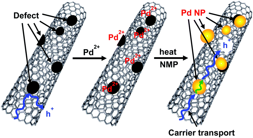 | ||
| Fig. 5 Schematic illustration of a defect repair reaction on SGCNTs, and carrier transports on the pristine SGCNT (left) and defect-repaired SGCNT (right). (Left): The pristine SGCNT having many defects, where a carrier is reflected on an interface of the defect. (Center): Adsorption of Pd2+ on defect sites of the SGCNT. (Right): Deposition of Pd NPs by a cumulative reduction of Pd2+s on the defect sites of the SGCNT, where the carrier transports on a surface of the repaired SGCNT through Pd NPs. | ||
The combination of two kinds of nanomaterials, i.e., CNTs and metal NPs, has introduced a novel “repairing effect” concept by coverage of the defective sites of the CNTs with NPs, resulting in enhancement of the electrical conductivity (from ∼90 S cm−1 to ∼165 S cm−1 at the Pd content of 10.8 wt%), which provided new TE materials with the high ZT value of ∼0.3 from inexpensive and defective CNTs (ZT ∼ 0.13). The high ZT value of ∼0.3, provided by the improvement in the carrier mobility while maintaining the carrier concentration, is one of the highest ZT values reported for practically applicable organic TE materials.14,15,28 In fact, at the maximum Pd content (17.4 wt%), the Seebeck coefficient (S) and electrical conductivity (σ) of the Pd@SGCNT hybrid sheet were ∼56 μV K−1 and ∼160 S cm−1, respectively, resulting in a power factor (PF) of ∼52 μW m−1 K−2. This strategy allows various NPs to self-locate at the exact defective sites in any type of nanomaterial like nanotubes, nanowires, and nanosheets. As the results, the coverage of metal NPs makes the defective nanomaterials behave as if they were defect-free ones. This technology based on the new concept of “defect repair” could provide not only inexpensive practical TE devices composed of repaired defective CNTs, but also extended applications of inexpensive and defective nanomaterials in various fields as a new electronic material, for examples, electrodes of solar cells and the lithium ion battery.
Conflicts of interest
There are no conflicts of interests to declare.Acknowledgements
K. Oshima and Y. Shiraishi are grateful to the Japan Society for the Promotion of Science (JSPS) for the funding supports through the Grant-in-Aid for Research Fellowship for Young Scientists, No. 17J11516, and Grant-in-Aid for Scientific Research (C), No. 15K04613 and 19K05633, respectively. This study was also financially supported by the New Energy and Industrial Technology Development Organization (NEDO), Japan, and Nippon ZEON Corporation, Japan.Notes and references
- S. Iijima and T. Ichihashi, Nature, 1993, 363, 603–605 CrossRef CAS.
- D. S. Bethune, C. H. Klang, M. S. de Vries, G. Gorman, R. Savoy, J. Vazquez and R. Beyers, Nature, 1993, 363, 605–607 CrossRef CAS.
- L. C. Venema, J. W. Janssen, M. R. Buitelaar, J. W. G. Wildöer, S. G. Lemay, L. P. Kouwenhoven and C. Dekker, Phys. Rev. B: Condens. Matter Mater. Phys., 2000, 62, 5238–5244 CrossRef CAS.
- A. Jorio, R. Saito, J. H. Hafner, C. M. Lieber, M. Hunter, T. McClure, G. Dresselhaus and M. S. Dresselhaus, Phys. Rev. Lett., 2001, 86, 1118–1121 CrossRef CAS.
- J. W. G. Wildöer, L. C. Venema, A. G. Rinzler, R. E. Smalley and C. Dekker, Nature, 1998, 391, 59–62 CrossRef.
- M. J. O’Connell, S. M. Bachilo, C. B. Huffman, V. C. Moore, V. C. Strano, E. H. Haroz, K. L. Rialon, P. J. Boul, W. H. Noon, C. Kittrell, J. Ma, R. H. Hauge, R. B. Weisman and R. E. Smalley, Science, 2002, 297, 593–596 CrossRef.
- S. J. Tans, A. R. M. Verschueren and C. Dekker, Nature, 1998, 393, 49–52 CrossRef CAS.
- A. D. Franklin, Science, 2015, 349(6249), aab2750 CrossRef.
- S. Diao, G. Hong, A. L. Antaris, J. L. Blackbum, K. Cheng, Z. Cheng and H. Dai, Nano Res., 2015, 8, 3027–3034 CrossRef CAS.
- S. N. Habisreutinger, R. J. Nicholas and H. J. Snaith, Adv. Energy Mater., 2017, 7, 1601839 CrossRef.
- C. Yu, Y. S. Kim, D. Kim and J. C. Grunlan, Nano Lett., 2008, 8, 4428–4432 CrossRef CAS.
- W. Zhao, S. Fan, N. Xiao, D. Liu, Y. Y. Tay, C. Yu, D. Sim, H. H. Hng, Q. Zhang, F. Boey, J. Ma, X. Zhao, H. Zhang and Q. Yan, Energy Environ. Sci., 2012, 5, 5364–5369 RSC.
- A. D. Avery, B. H. Zhou, J. Lee, E.-S. Lee, E. M. Miller, R. Ihly, D. Wesenberg, K. S. Mistry, S. L. Guillot, B. L. Zink, Y.-H. Kim, J. L. Blackburn and A. J. Ferguson, Nat. Energy, 2016, 1, 16033 CrossRef CAS.
- N. Toshima, Synth. Met., 2017, 225, 3–21 CrossRef CAS.
- J. L. Blackburn, A. J. Ferguson, C. Cho and J. C. Grunlan, Adv. Mater., 2018, 30, 1704386 CrossRef.
- S. Lee, S. Kim, A. Pathak, A. Tripathi, T. Qiao, Y. Lee, H. Lee and H. Y. Woo, Macromol. Res., 2020, 28, 531–552 CrossRef CAS.
- I. Petsagkourakis, K. Tybrandt, X. Crispin, I. Ohkubo, N. Satoh and T. Mori, Sci. Technol. Adv. Mater., 2018, 19, 836–862 CrossRef CAS.
- O. Caballero-Calero and M. Martin-Gonzalez, Scr. Mater., 2016, 111, 54–57 CrossRef CAS.
- N. Nandihalli, C.-J. Liu and T. Mori, Nano Energy, 2020, 78, 105186 CrossRef CAS.
- M. Martin-Gonzalez, O. Caballero-Calero and P. Diaz-Chao, Renewable Sustainable Energy Rev., 2013, 24, 288–305 CrossRef CAS.
- R. Tian, C. Wan, N. Hayashi, T. Aoai and K. Koumoto, MRS Bull., 2018, 43, 193–198 CrossRef CAS.
- S. Shaikh, K. Lafdi and E. Silverman, Carbon, 2007, 45, 695–703 CrossRef CAS.
- Y. Nakai, K. Honda, K. Yanagi, H. Kataura, T. Kato, T. Yamamoto and Y. Maniwa, Appl. Phys. Express, 2014, 7, 025103 CrossRef.
- M. Piao, M.-K. Joo, J. Na, Y.-J. Kim, M. Mouis, G. Ghibaudo, S. Roth, W.-Y. Kim, H.-K. Jang, G. P. Kennedy, U. Dettlaff-Weglikowska and G.-T. Kim, J. Phys. Chem. C, 2014, 118, 26454–26461 CrossRef CAS.
- C. Yu, K. Choi, L. Yin and J. C. Grunlan, ACS Nano, 2011, 5, 7885–7892 CrossRef CAS.
- K. Suemori, Y. Watanabe and S. Hoshino, Appl. Phys. Lett., 2015, 106, 113902 CrossRef.
- K. Oshima, Y. Shiraishi and N. Toshima, Chem. Lett., 2015, 44, 1185–1187 CrossRef CAS.
- N. Toshima, K. Oshima, H. Anno, T. Nishinaka, S. Ichikawa, A. Iwata and Y. Shiraishi, Adv. Mater., 2015, 27, 2246–2251 CrossRef CAS.
- C. Cho, B. Stevens, J.-H. Hsu, R. Bureau, D. A. Hagen, O. Regev, C. Yu and J. C. Grunlan, Adv. Mater., 2015, 27, 2996–3001 CrossRef CAS.
- K. Hata, D. N. Futaba, K. Mizuno and T. Namai, Science, 2004, 306, 1362–1364 CrossRef CAS.
- W. Wang, S. Sun, S. Gu, H. Shen, Q. Zhang, J. Zhu, L. Wang and W. Jiang, RSC Adv., 2014, 4, 26810–26816 RSC.
- N. Toshima, Pure Appl. Chem., 2013, 85, 437–451 CAS.
- N. Toshima, N. Jiravanichanun and H. Marutani, J. Electron. Mater., 2012, 41, 1735–1742 CrossRef CAS.
- R. Gangopadhyay and A. De, Chem. Mater., 2000, 12, 608–622 CrossRef CAS.
- K.-Y. Chun, Y. Oh, J. Rho, J.-H. Ahn, Y.-J. Kim, H. R. Choi and S. Baik, Nat. Nanotechnol., 2010, 5, 853–857 CrossRef CAS.
- C. Yu, Y. Ryu, L. Yin and H. Yang, ACS Nano, 2011, 5, 1297–1303 CrossRef CAS.
- K. Choi and C. Yu, PLoS One, 2012, 7, e44977 CrossRef CAS.
- G. E. Fernandes, J. H. Kim and J. Xu, Mater. Res. Bull., 2013, 48, 2950–2954 CrossRef CAS.
- C. J. An, Y. H. Kang, A.-Y. Lee, K.-S. Jang, Y. Jeong and S. Y. Cho, ACS Appl. Mater. Interfaces, 2016, 8, 22142–22150 CrossRef CAS.
- K. Oshima, J. Inoue, S. Sadakata, Y. Shiraishi and N. Toshima, J. Electron. Mater., 2017, 46, 3207–3214 CrossRef CAS.
- H. Hirai, Y. Nakao and N. Toshima, J. Macromol. Sci., Chem., 1979, A13, 727–750 CrossRef.
- N. Toshima and T. Yonezawa, New J. Chem., 1998, 22, 1179–1201 RSC.
- H. Zhang, T. Watanabe, M. Okumura, M. Haruta and N. Toshima, Nat. Mater., 2012, 11, 49–52 CrossRef.
- Z. Liu, J. Y. Lee, W. Chen, M. Han and L. M. Gan, Langmuir, 2004, 20, 181–187 CrossRef CAS.
- Y. Xing, J. Phys. Chem. B, 2004, 108, 19255–19259 CrossRef CAS.
- P. V. Kamat, J. Phys. Chem. Lett., 2010, 1, 520–527 CrossRef CAS.
- S. Yang, J. Dong, Z. Yao, C. Shen, X. Shi, Y. Tian, S. Lin and X. Zhang, Sci. Rep., 2014, 4, 4501 CrossRef.
- A. P. Leggiero, K. J. Trettner, H. L. Ursino, D. J. McIntyre, M. Schauer, E. Zeira, C. D. Cress and B. J. Landi, ACS Appl. Nano Mater., 2019, 2, 118–126 CrossRef CAS.
- M. N. Tchoul, W. T. Ford, G. Lolli, D. E. Resasco and S. Arepalli, Chem. Mater., 2007, 19, 5765–5772 CrossRef CAS.
- T. Fujigaya and N. Nakashima, Adv. Mater., 2013, 25, 1666–1681 CrossRef CAS.
- J. Kastner, T. Pichler, H. Kuzmany, S. Curran, W. Blau, D. N. Weldon, M. Delamesiere, S. Draper and H. Zandbergen, Chem. Phys. Lett., 1994, 221, 53–58 CrossRef CAS.
- Y. Miyata, K. Mizuno and H. Kataura, J. Nanomater., 2011, 2011, 786763 Search PubMed.
- Y. Inoue, Y. Suzuki, Y. Minami, J. Muramatsu, Y. Shimamura, K. Suzuki, A. Ghemes, M. Okada, S. Sakakibara, H. Mimura and K. Naito, Carbon, 2011, 49, 2437–2443 CrossRef CAS.
- N. Toshima and N. Jiravanichanun, J. Electron. Mater., 2013, 42, 1882–1887 CrossRef CAS.
- A. Yoshida and N. Toshima, J. Electron. Mater., 2014, 43, 1492–1497 CrossRef CAS.
- A. Yoshida and N. Toshima, J. Electron. Mater., 2016, 45, 2914–2919 CrossRef CAS.
- S. Hata, T. Omura, K. Oshima, Y. Du, Y. Shiraishi and N. Toshima, Bull. Soc. Photogr. Imag. Jpn., 2017, 27, 13–18 Search PubMed.
- H. Hirai, H. Chawanya and N. Toshima, React. Polym., 1985, 3, 127–141 CAS.
- J. R. Szczech, J. M. Higgins and S. Jin, J. Mater. Chem., 2011, 21, 4037–4055 RSC.
- T. Mori, Small, 2017, 13, 1702013 CrossRef.
- T. Mori and T. Hara, Scr. Mater., 2016, 111, 44–48 CrossRef CAS.
- T. Yonezawa and N. Toshima, J. Chem. Soc., Faraday Trans., 1995, 91, 4111–4119 RSC.
Footnote |
| † Electronic supplementary information (ESI) available: TEM, SEM of hybrid sheets by physical mixtures, Pd content dependence of TE factors, image of Marshal's baton, Raman spectra, XPS, electrical conductivity vs. Pd content curves (figures and table), SEM of Pd@SGCNT sheets, and thermal conductivity through plane in table. See DOI: 10.1039/d0ma00534g |
| This journal is © The Royal Society of Chemistry 2020 |