
 Open Access Article
 This Open Access Article is licensed under a Creative Commons Attribution-Non Commercial 3.0 Unported Licence
Tuning the morphology of manganese oxide nanostructures for obtaining both high gravimetric and volumetric capacitance†
Jones de A.
Pereira
a,
Janiny N.
Lacerda
a,
Izabella F.
Coelho
a,
Cauê de S. C.
Nogueira
b,
Dante F.
Franceschini
a,
Eduardo A.
Ponzio
 c,
Fernando B.
Mainier
a and
Yutao
Xing
*b
c,
Fernando B.
Mainier
a and
Yutao
Xing
*b
aDepartamento de Engenharia Química e de Petróleo, Universidade Federal Fluminense, 24210-346, Niterói, RJ, Brazil
bLaboratório de Microscopia Eletrônica de Alta Resolução, Centro de Caracterização Avançada para Indústria de Petróleo (LaMAR/CAIPE), Universidade Federal Fluminense, 24210-346, Niterói, RJ, Brazil. E-mail: xy@id.uff.br
cGrupo de Eletroquímica e Eletroanalítica (G2E), Instituto de Química, Universidade Federal Fluminense, Campus Valonguinho, 24020-141, Niterói, RJ, Brazil
First published on 2nd September 2020
Abstract
Obtaining both high gravimetric capacitance (Cs_m) and high volumetric capacitance (Cs_V) in supercapacitors is still a great challenge. We prepared manganese oxide (MO) nanostructures by pulsed laser deposition, using a metallic Mn target in an O2 atmosphere with pressures ranging from 0.1 Torr to 2.0 Torr at room temperature. The morphology gradually changed from a dense film to nanofoam with different porosities and densities. Raman spectroscopy and X-ray photoelectron spectroscopy revealed a similar oxidation state despite distinct microstructures. Cs_m and Cs_V for the three typical nanostructures, namely thin films, perpendicular columnar structures and nanofoams, were compared. It was found that the highest Cs_m value was not obtained in the nanofoam sample with the highest porosity, but it was achieved in the sample with a perpendicular columnar structure with a Cs_m value of 976 F g−1 at 5 mV s−1. Such a configuration showed the highest Cs_V as well with a value of 830 F cm−3 at 5 mV s−1. The best performance with voltage scan rates higher than 50 mV s−1 was found in the nanofoam structures with the values of 612 F g−1 at 100 mV s−1 and 352 F g−1 at 300 mV s−1. Our research gives useful suggestions for material design in supercapacitor electrodes: a suitable microstructure can be used for applications focusing on different parameters of a supercapacitor. The results might be of general interest for the energy storage research community.
1 Introduction
Supercapacitors are promising energy storage devices with desirable properties such as long life-time, high power density and faster charge/discharge rate, which fill well the gap between conventional capacitors and batteries.1–3 The most commonly used electrode materials are active carbon materials4,5 (graphenes,6 nanotubes,7 and carbon materials obtained from biomass8), conducting polymers,9 metallic nanoparticles,10 transition metal oxides and selenides,11–13 and composite materials.14–17 Manganese oxides (MOs) have been widely studied as electrode materials, due to their high energy storage capacity, abundancy in nature and low cost.18–20 MOs can exist in several oxidation states (Mn2+, Mn3+ and Mn4+), forming different oxides, such as MnO, Mn3O4, Mn2O3 and MnO2.21,22 The most commonly used MO for supercapacitors is MnO2,20,23 but other oxides like Mn3O4 have been more and more investigated.24 The gravimetric capacitance (Cs_m) obtained for the pure Mn3O4 phase25 is 401 F g−1 at 10 mV s−1 and for the Mn2O3 crystalline phase, the value is 460 F g−1 at 10 mV s−1.26Despite many advantages, MOs do not undergo fast ion diffusion in the bulk form, and thus the pseudo-capacitance is mainly provided by surface reactions.27 Therefore, the performance of MOs as supercapacitor electrodes is dominated by a specific surface area27 and for this reason, nanostructured MOs are usually used as supercapacitor electrodes. Nanostructured electrodes can be prepared by different methods, for example, chemical and electrochemical methods,18,28 electrophoretic deposition,29 physical vapor deposition30 sol–gel methods,31,32 hydrothermal methods33 and successive ionic layer adsorption and reaction methods.34,35 Pulsed laser deposition (PLD) in the presence of a buffer gas has been reported as a versatile tool for fabricating nanoparticles and other nanostructures with controlled size.36–38 This technique is used to synthesize MO electrodes as well.39–42 Yang synthesized MOs using manganese metallic and Mn3O4 targets in an O2 atmosphere with pressures ranging from 1 mTorr to 0.5 Torr and obtained crystalline phases of Mn2O3, Mn3O4 and amorphous MnOx.43 With the background gas pressures being higher than those used for the production of nanoparticles, a new type of nanostructure, namely nanofoam, can be fabricated, with a highly porous and interconnected foam-like morphology.44–46 Nanofoams of different materials, such as carbon44,45 and metal oxides (ZnO, TiO2, SnO2 and MoO3),46 have been produced by PLD.
Due to the progress in the study of nanostructured materials, the performance of supercapacitors has been continuously improved as a result of the larger surface area and better activity of electrode materials. However, the high specific surface area usually comes together with a low packing density, which results in a large volume occupancy of the produced devices. Huan Li et al. discussed the importance of volumetric capacitance (Cs_V) and studied methods to quantify the volumetric performance of supercapacitors.47 Zhuangnan Li et al. reported that a maximum Cs_V can be achieved when the pore sizes match the diameter of the electrolyte ions by tuning the interlayer spacing of freestanding graphene laminate films.48 Our group recently reported the production of MO nanofoams by PLD, which showed a very large specific surface area and a high specific capacitance as electrodes in supercapacitors.41 However, there are still several points which are unclear or can be improved for the understanding of the MO nanofoam: first, the MO nanofoam shows a large surface area but a small density, i.e., although its Cs_m is high, its Cs_V is quite low. Second, there is an activation process within the first 200 cycles whose mechanism is still not very clear. Last, there is still space to improve the mechanical properties by increasing the density and strengthening the connection between the MO nanoparticles that build the MO nanoform. As discussed above, Cs_m and Cs_V are closely related to the density and the specific surface area of the nanostructures, and hence high Cs_m is usually accompanied with low Cs_V and vice versa. In order to obtain both high Cs_m and Cs_V in a supercapacitor, nanomaterials with a suitable density are desirable. However, it is still a challenge to produce nanostructures with a controlled particle and pore size. By using PLD, it is practically simple to change the pressure in the PLD chamber and consequently, to tune the density of the prepared nanostructures in a straightforward way.49–52 The oxidation state of the transition metal oxides prepared by this method is expected to be similar, and thus one can focus on the pure morphology effect on the supercapacitive properties.
In this work, we report on the synthesis and characterization of MO nanostructures by PLD with a tunable microstructure, driven by only one parameter: the background gas pressure. How the gas pressure affects the microstructure and the deposition rate will be discussed in this work. We aim at the fabrication of a suitable nanostructure showing both high Cs_m and Cs_V. The purely morphological effect on the supercapacitive properties is the main objective of this investigation.
2 Methods
The MO nanofoam was prepared by PLD from a metallic Mn target in the presence of O2 with a pressure range of 0.1, 0.5, 1.0 and 2.0 Torr at room temperature (the samples are named as MO01, MO05, MO10 and MO20). The deposition conditions and other parameters for the samples are listed in Table S1 in the ESI.† Target ablation was done using the first harmonic (1064 nm wavelength) of a pulsed Nd:YAG laser with 200 mJ energy of each pulse, 0.12 J mm−2 energy density, 7 ns pulse duration and 10 Hz repetition rate. The beam was focused onto the Mn target with an incidence angle of 45° and the ablated Mn plume expanded in the direction of the substrate, which was mounted on a sample holder, at a fixed 3.5 cm distance from the target. Samples for structure and morphology studies were deposited over Si single crystal wafers (100) and samples for electrochemical studies were prepared over stainless-steel sheets as substrates, with the deposition time fixed for 30 minutes duration. The deposition rates were measured with a quartz crystal balance mounted inside the PLD vacuum chamber. The as-prepared samples were then heat-treated in air for 90 minutes at 300 °C in order to improve the mechanical bonding properties. The morphology and thickness of the samples were investigated with field-emission scanning electron microscopy (SEM: JEOL JSM 7100F). The chemical composition and the electronic structure of the products were characterized by Raman spectroscopy (Witec alpha 300 Raman spectrometer, 532 nm wavelength excitation) and X-ray photoelectron spectroscopy (XPS: a Thermo Scientific ESCALAB 250XI spectrometer with monochromatized Mg-Kα radiation). A typical three-electrode glass cell equipped with a working electrode (stainless steel with manganese oxide deposited), a platinum foil counter electrode, and a Ag|AgCl (3 M) reference electrode was used for electrochemical measurements. Cyclic voltammetry (CV) was performed using an electrochemical workstation (Ivium Technologies model: IviumnStat) in a 0.1 M Na2SO4 aqueous solution.3 Results and discussion
Fig. 1(a) shows the deposition rates of MO measured with the quartz balance. We could see that the deposition rates decreased with the increasing pressure. Fig. 1(c) and (d) illustrate the laser ablation process in vacuum and with the background gas in the chamber. When the laser pulse reached the target surface, it evaporated atoms and small clusters of the target material with a quite high speed inside the plasma plume and they could deposit on the substrate with plume expansion. In vacuum, the mean-free-path of the atoms is much higher than the target-substrate distance. As a result, the atoms could arrive at the substrate with very low collision probability [see Fig. 1(c)]. This process resulted in the formation of compact thin films. The presence of the gas in the chamber decreased the mean-free-path of the atoms and generated collisions and reactions between the ablated atoms and gas molecules. This process decreased the velocity of the atoms and those lower energy atoms interacted and consequently generated nanoparticles before they arrived at the substrate as shown in Fig. 1(d). Due to the collision processes, which led to plume scattering, the deposition rates decreased with the increasing pressure. The mass of the active materials on the electrodes was obtained with the deposition rates and the area of the electrodes.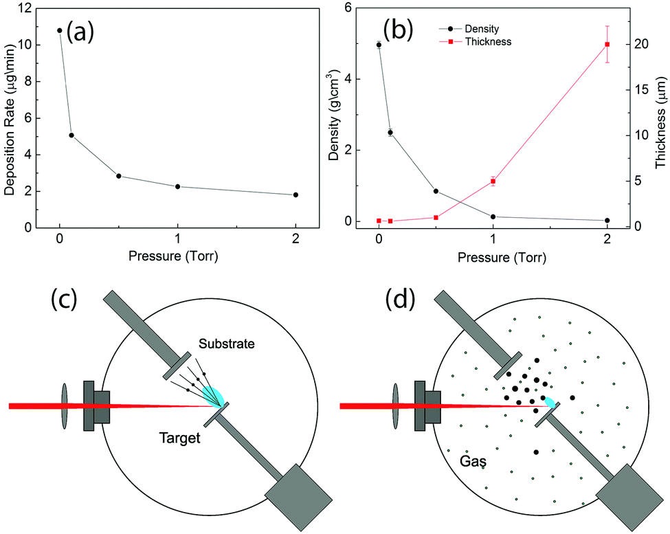 | ||
| Fig. 1 (a) Deposition rates measured by the quartz balance as a function of pressure in the chamber. (b) Densities and thicknesses of the samples as a function of pressure. Schematic illustration of the deposition process (c) in vacuum and (d) with the background gas. The black dots in (c) and the bigger black dots in (d) indicate Mn atoms and nanoparticles, respectively. The smaller gray dots in (d) illustrate the gas molecules in the chamber. | ||
From the above discussion we know that the pressure in the PLD chamber determines the microstructure of the deposited materials, for example, thin films can be obtained in vacuum53 and the nanofoam can be formed with 5 Torr of O2.41 Thus, it is simple to tune the density of the deposited materials gradually by changing the pressure in the PLD chamber. For the samples prepared in this work, the thickness measured with the cross-section SEM images and the density calculated with the mass and the volume as a function of gas pressure are shown in Fig. 1(b). Their values can be found in Table S1 of the ESI.† A less thickness increase is observed when the pressure increased to 0.5 Torr. From then on, the thickness of the prepared material increased very rapidly with the increase of the pressure. The density of the samples, on the other hand, shows an opposite behavior. It shows a very fast decrease when the pressure changes from 10−6 Torr to 1 Torr. Since the main goal of this work is to study the morphology effect and consequently to find a suitable structure of MO with both high Cs_m and Cs_V, the pressure range between 0 and 2 Torr is thus sufficient for the present study.
In this work, the presence of the background gas O2 served not only as collision media but also as a reaction source, resulting in the formation of MO nanoparticles. A complete understanding of the oxidation state of manganese was necessary, and therefore the electrical structures were studied with Raman spectroscopy and XPS.
Fig. 2(a) shows the most relevant portion of the Raman spectra obtained from the studied samples, since no features were observed at higher wavenumbers. The vertical lines in the graph designated the positions of α-MnO2 (solid lines) and tetragonal Mn3O4 (dashed line). The spectra were similar and noisy, as can be observed. In fact, better spectra could be obtained with a higher laser power. However, the oxidation states were modified by stronger laser radiation in the major presence of Mn3O4. In this case, a very low laser density was applied during the spectrum collection and the accumulating time for each spectrum was more than 8 hours. Since all the spectra showed some features of the MnO2 Raman spectrum, we associated the weak spectra to the dominance of this oxide in the samples. In addition, the spectra were also compatible with the presence of Mn3O4, probably due to partial damage of the sample by the incident laser. The mean peak of MO20 was fitted with the Raman shift of MnO2 and Mn3O4 as shown in Fig. 2(b). This clearly demonstrated that most of the Raman scattering was from MnO2 (634 cm−1 and 512 cm−1) and the intensity of the Mn3O4 (657 cm−1) scattering was very low. However, the integrated intensity ratio of MnO2 and Mn3O4 does not correspond to the real proportion of the two oxides in the sample due to different Raman scattering probabilities for different manganese oxides. It is well known that MnO2 has a much smaller Raman activity, as compared to other manganese oxides.54 So there was even less Mn3O4 in the deposited material than what the Raman spectrum indicated. Considering the above discussion, we can conclude that the samples had very similar structures, majorly composed of MnO2.
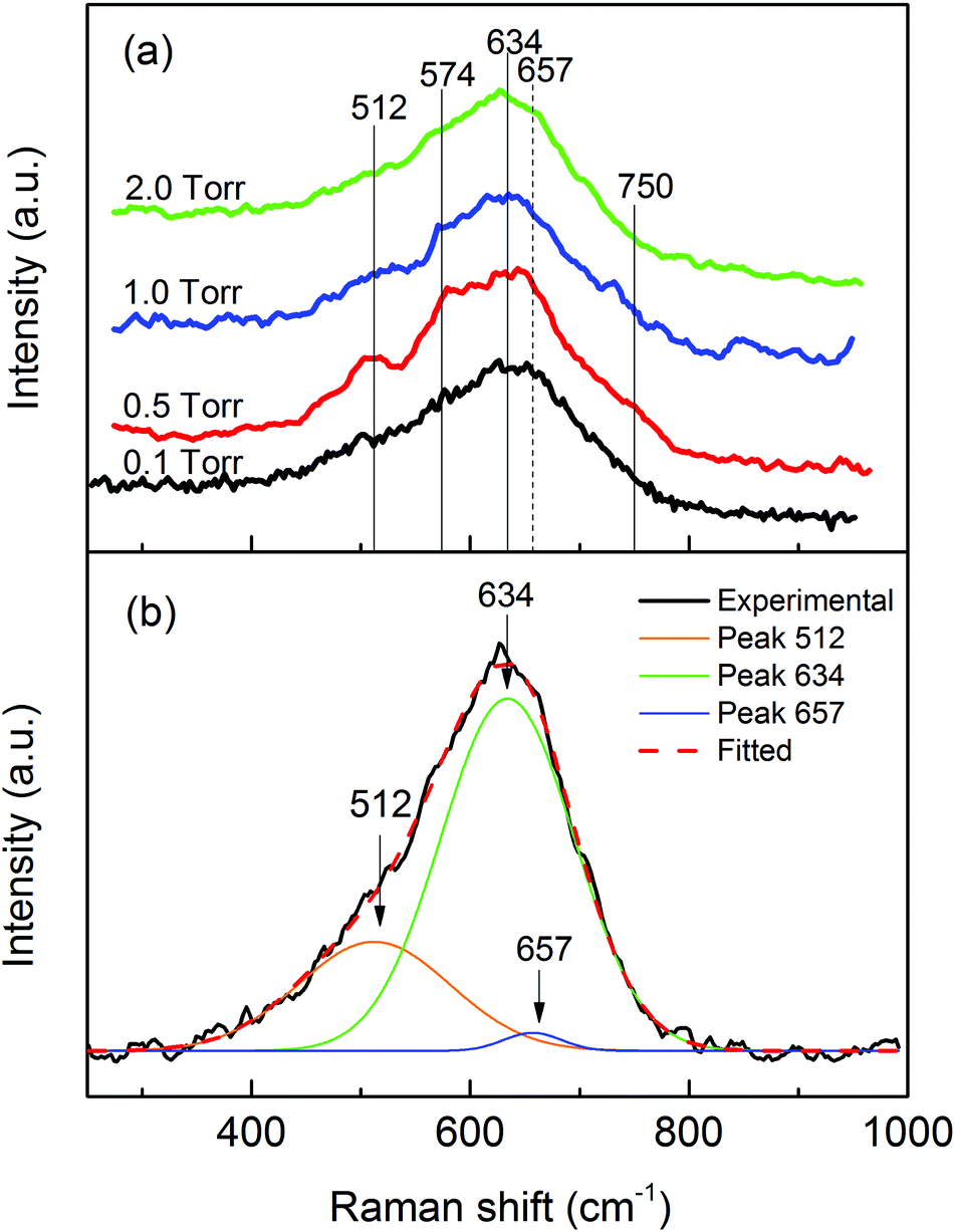 | ||
| Fig. 2 (a) Raman spectra of the MO samples. The vertical lines indicate the position of the main peaks of α-MnO2 (solid lines) and tetragonal Mn3O4 (dashed line). (b) Deconvolution of the main peak for the sample MO20. | ||
Fig. 3 shows the XPS Mn 2p and O 1s spectra of the samples studied in this work. The Mn 2p spectra were placed at the same minimum background level, and normalized to the maximum intensity of the higher peak, in order to make the comparison easier. The O 1s spectra were, instead, Shirley background subtracted and normalized to the maximum intensity of the higher peak, for the same purpose. The Mn 2p spectra of the four samples were practically identical, with the Mn 2p1/2 peak maximum located in the 642.2–642.25 eV region and the Mn 2p3/2 peak maximum located in the 653.8–654.05 eV range. These peak positions were compatible with those reported for a-MnO2 by Gu et al.,55 at 644.2 eV and 653.8 eV, respectively, in accordance with the Raman results. On the other hand, the O 1s spectra showed small to moderate differences in shape. To analyze them we should consider the presence of the O–Mn–O, Mn–O–H and H–O–H peaks located at about 529.7 eV, 530.5 eV and 531.5 eV. In order to get information on the Mn oxidation state, we analyzed the O 1s spectra by fitting the above-mentioned peaks to the Shirley background subtracted O 1s spectra (see the fitting results in the ESI†). We estimated the Mn oxidation number by using the O–Mn–O and Mn–O–H and H–O–H peak areas, within the procedure suggested by Tholkappiyan et al.56 We obtained the oxidation numbers for the samples from 0.5 to 2 Torr to be equal to 2.8, 2.7, 2.9, and 3.2, respectively. The oxidation numbers of the three samples were situated in the 2.9 ± 0.3 range, constituting a relatively small variation. The expected value of the oxidation number for MnO2 should be near 4.0 and the origin of the smaller oxidation number in our samples is unclear. With the results we can conclude that the sampes had similar oxidation states, which was consistent with the minor difference observed in the Raman spectra and the Mn 2p XPS spectra. Apparently all the samples had very similar electronic structures and compositions.
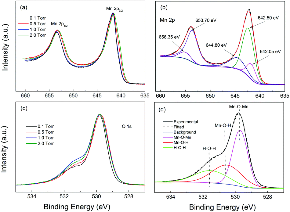 | ||
| Fig. 3 (a) High resolution XPS spectra of Mn 2p for the MO samples. (b) Deconvolution of the Mn 2p spectrum for MO10. (c) High resolution XPS spectra of O 1s for the samples. (d) Deconvolution of the O 1s spectrum for MO10. | ||
The morphology of the MO nanostructures was investigated by SEM and the images are shown in Fig. 4. The surface of MO01 was quite flat with several spheres on top. The high resolution image revealed that the sample was formed by nanoparticles with size less than 10 nm. The cross-section image showed that the film was still quite dense with a thickness of ∼600 nm although it was formed by nanoparticles. When the pressure increased to 0.5 Torr, the MO05 sample showed a very rough, cracked surface with big balls on it. From the high resolution image one could see that the surface had a cauliflower-like morphology, and that each big ball on the surface was constructed by nanoparticles. The observed cracks were the voids between the big balls. From the cross-section image one could see that the cracks came from the sample surface to the substrate, and the sample showed a perpendicular columnar structure with a 150 nm mean column diameter. The measured thickness was about 1 μm, bigger than that of MO01, which corresponds to the decreased density. With 1.0 Torr O2 pressure inside the chamber, the density of MO10 decreased even more. The surface of the sample still showed the presence of big balls as in MO05, but with a larger distance between the nanoparticles. The cross section image exhibited a tree-like structure in the perpendicular direction and the thickness reached about 5 μm. When the O2 pressure increased to 2.0 Torr, the microstructure was nanofoam-like with a very low density, as reported before.41 The nanofoam was constructed by nanofilaments, which were assemblies of nanoparticles. The thickness of this sample was as high as ∼25 μm although it had less material compared with other samples. No obvious texture was observed in this sample. The thicknesses would be used to calculate the volumes of the active materials on the electrodes.
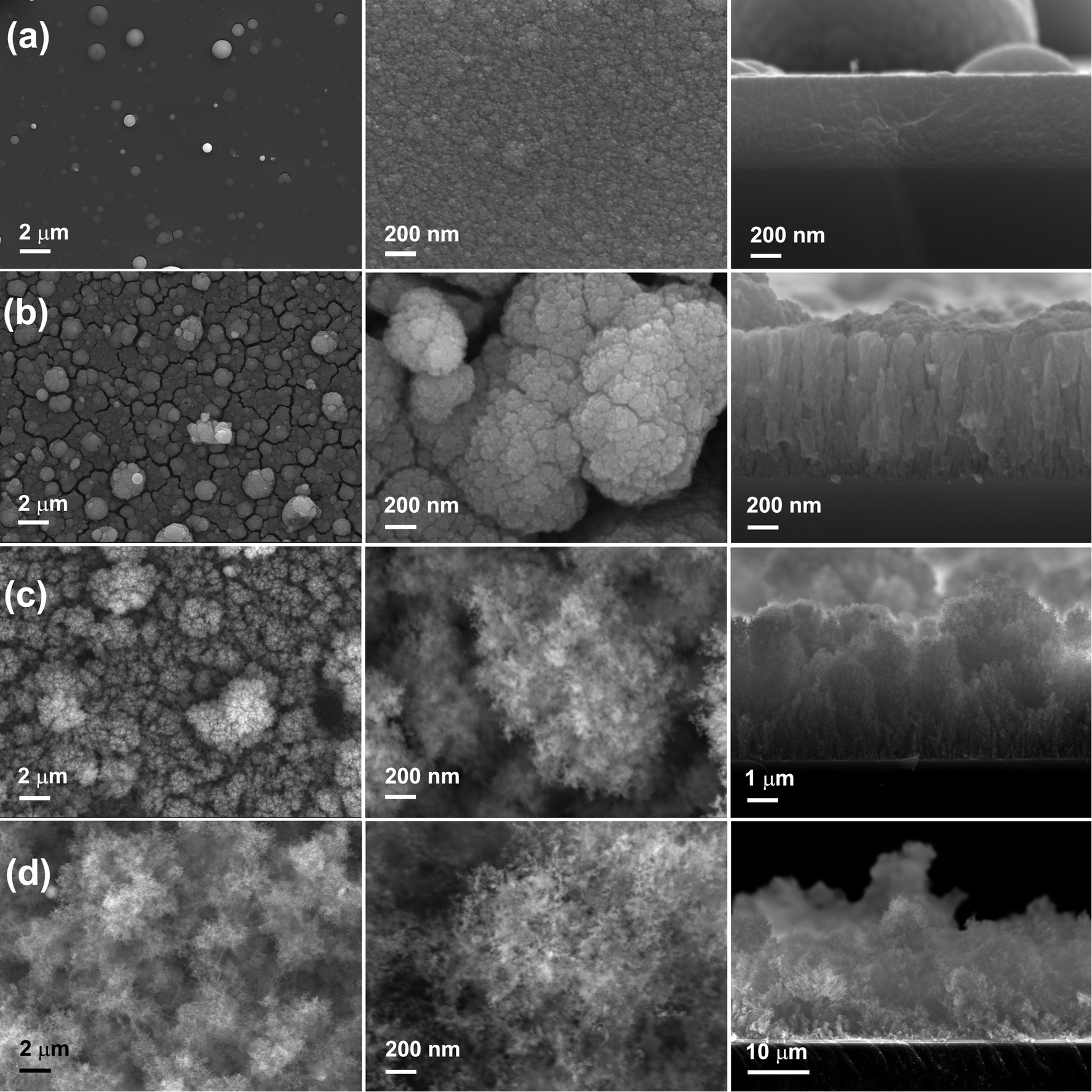 | ||
| Fig. 4 SEM images of the MO nanostructures prepared by PLD with gas pressures of (a) 0.1 Torr, (b) 0.5 Torr, (c) 1.0 Torr and (d) 2.0 Torr. The left row is the low magnification; in the middle, the high magnification and the right, the cross-section images. | ||
The mechanism of the different structure formation was as follows. As shown in Fig. 1(c), the vaporized atoms by the laser pulse possessed very high energy and they deposited directly onto the substrate. The impact of the atoms was very high, and furthermore the atoms could form chemical bonds only with the deposited materials on the substrate since most of the materials arriving at the substrate were single atoms. As a result, thin films could be obtained in vacuum. With the gas molecules in the chamber, as shown in Fig. 1(d), the collision among the atoms and gases greatly decreased the energy of the atoms and as a result, the atoms formed nanoparticles before reaching the substrate. At the same time, the velocity of the nanoparticles was much less than the single atoms in vacuum. The nanoparticles with less energy had much less impact energy on the substrate and this resulted in the formation of less dense materials than the thin films. With an even higher pressure, due to more scattering and an even lower velocity, the nanoparticles could move to different directions and they were able to find low energy positions, which were sharp points on the surface. The sharp ends on the surface always have a higher statistic charge to attract the nanoparticles during deposition. As a result, the nanoparticles formed filaments, and furthermore nanofoams. Detailed microstructural studies demonstrate a crystalline structure of similar MO samples.41
After understanding the morphology and the oxidation states, we studied the supercapacitive properties by cyclic voltammetry (CV) in a 0.1 M Na2SO4 aqueous solution with a three-electrode system. The representative CV curves of the MO electrodes over a range of scan rates from 5 to 350 mV s−1 could be found in the ESI.† The CV curves exhibited typical charge and discharge hysteresis as we expected, indicating the kinetic reversibility of the redox process. We estimated the capacitive behaviors of the MO electrode from the CV curves, by calculating the charge during the anodic and cathodic scan. The calculated Cs_m and Cs_V values are shown in Fig. 5. The four samples demonstrated a huge Cs_m difference both at low and high scan rates, with variations from 200 to 1000 F g−1 at a scan rate of 5 mV s−1 and 30 to 300 F g−1 at 350 mV s−1, as shown in Fig. 5(a). The MO01 showed the lowest Cs_m value in the range of all the scan rates. The Cs_m of MO20 was much higher than that of MO01 but lower than those of both MO05 and MO10. The two samples, namely, MO05 and MO10, showed a high Cs_m value but with a different behavior as a function of scan rate. With the scan rates ranging from 5 to 25 mV s−1, the MO05 had higher Cs_m than MO10 and above 25 mV s−1, the MO10 became better and the Cs_m value (315 F g−1) was 60% higher than that of MO05 (190 F g−1) at a scan rate of 350 mV s−1.
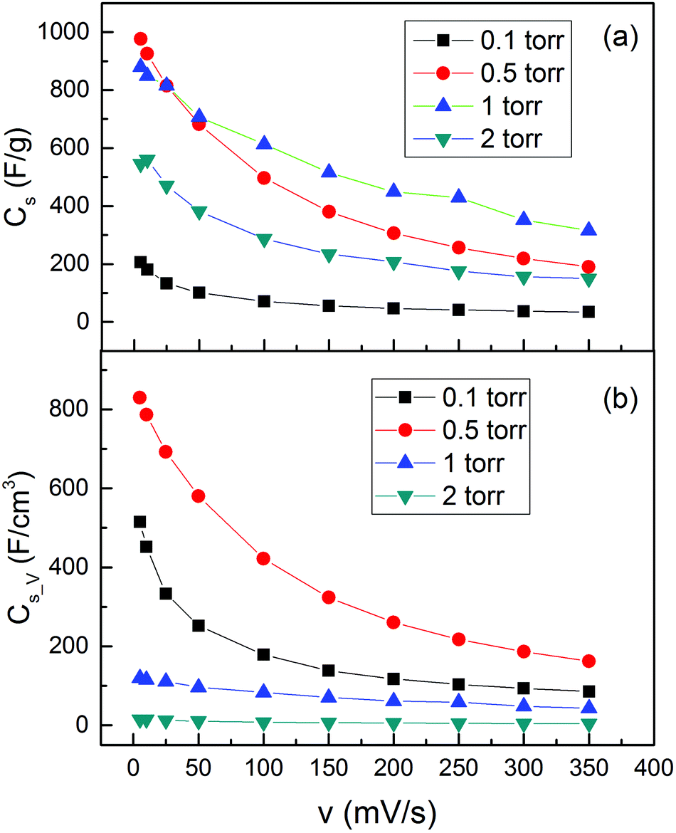 | ||
| Fig. 5 (a) Gravimetric capacitance (Cs_m) and (b) volumetric capacitance (Cs_V) as a function of voltage scan rate for the MO nanostructures. | ||
The Cs_V values, however, showed very different behavior compared with the Cs_m value, as shown in Fig. 5(b). The volume of each sample was obtained by the area and thickness of the active material and the values can be found in Table S1 of the ESI.† Although MO20 had a very high Cs_m, it had the lowest Cs_V due to the sponge-like morphology with an extremely low density. MO10 exhibited the highest Cs_m above the voltage scan rate of 50 mV s−1; however, it had even lower Cs_V than that of MO01, the one with the lowest Cs_m. The highest Cs_V was found in the sample MO05, which had the highest Cs_m below the voltage scan rate of 50 mV s−1 as well. A comparison of the MO01 and MO05 samples in Fig. 5(b) shows that the Cs_V of MO01 decreased much faster than that of MO05, for example, from 515 F cm−3 at 5 mV s−1 to 251 F cm−3 at 50 mV s−1 for MO01, it decreased by more than 50%. The Cs_V values were 830 F cm−3 at 5 mV s−1 and 580 F cm−3 at 50 mV s−1 for MO05, and decreased by only ∼30%.
Usually the theoretical values of the specific capacitance are determined by the intrinsic properties of the active electrode materials for supercapacitors. The real specific capacitance, on the other hand, depends strongly on the morphologies. In this work, the MO samples are all with similar oxidation states, as can be derived from the Raman and XPS spectra. The most robust difference for them is the morphology, and therefore the different Cs_m and Cs_V values observed in the present work are closely related to the morphologies of the different nanostructures. In order to get a better understanding, we separated the electrical double layer capacitance (EDLC) and the diffusion controlled pseudocapacitance for the three typical electrodes with the Trasatti method57–59 and for different voltage scan rates with the Dunn method.60,61 The results are presented in Fig. 6, together with schematic illustrations of the three typical corresponding microstructures observed in this work. The detailed calculations can be found in the ESI.† As can be seen in Fig. 6(a), the capacitive contribution significantly increased from 8.1% for the thin film sample MO01 to 87.1% for the nanofoam sample MO10. By changing the scan rates, for example, in MO10 as shown in Fig. 6(b), the capacitive contribution increased upon increasing the voltage scan rate, from ∼8% with a scan rate of 10 mV s−1 to ∼34% with a scan rate of 350. The values shown in Fig. 6(a) were obtained by the Trasatti Method under the conditions of the voltage scan rate v → 0 and v → ∞ and that is why they are different from the results for the intermediate scan rates shown in Fig. 6(b), which have been calculated with the Dunn method. The significant increase of the capacitive contribution in this work is due to the increase of the specific surface areas for the different nanostructures, as can be clearly seen from the SEM images. The values of the specific surface area vary from several m2 for the thin films (estimated by supposing a thin film with 600 nm of thickness) to ∼150 m2 for the nanofoam measured by N2 adsorption.41 We will discuss the detailed morphology effects further on the capacitive contribution in the three nanostructures.
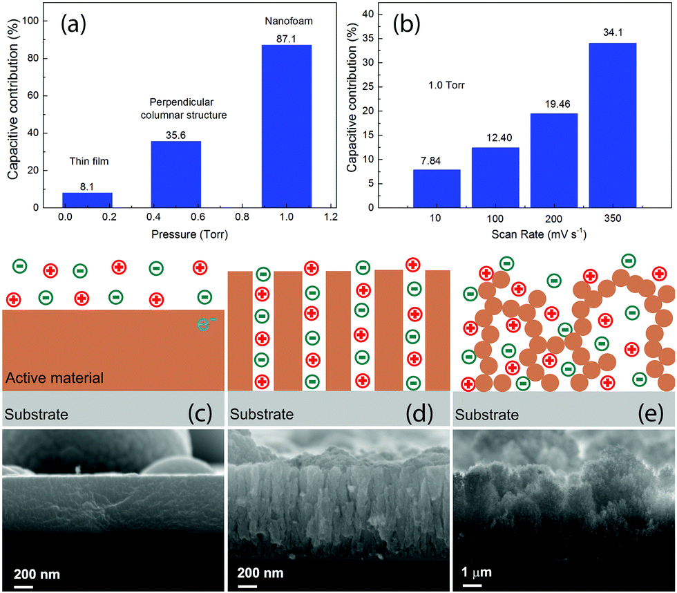 | ||
| Fig. 6 (a) Capacitive contribution for the samples representing the three typical nanostructures. (b) Capacitive contribution at different voltage scan rates for MO10, which has a nanofoam structure. Schematic illustration of the electrodes for (c) MO01, (d) MO05 and (e) MO10 with different morphologies of the active materials, as indicated by the SEM images below. The circles with + and − signals inside indicate positive and negative ions. | ||
As is well known, there are two different processes for the charge storage mechanism for MO-based supercapacitors: capacitive contribution associated with the adsorption/desorption (a/d) process that occurs at the electrode surface and/or diffusion controlled contribution associated with the insertion/extraction (i/e) process that happens in the electrode bulk.62,63 The a/d process dominates in the MO samples with a high surface area, whereas the i/e process occurs mostly in crystalline MO compounds.62,63 For 2D materials with only one dimension in the nanometer scale, such as thin films, as shown in Fig. 6(c), the positive and negatives ions were in touch with the active materials only from one side. Such a configuration had a less surface area, which leads to less capacitive contribution and diffusion controlled pseudocapacitance dominates. As a result, it had the lowest Cs_m. Since the active material was quite dense, the Cs_V of such a sample was not as bad as Cs_m.
The perpendicular columnar structure, as shown in Fig. 6(d), had a higher specific surface area than the thin films. The positive and negative ions were surrounding each pillar in this configuration. The mean diameter of the pillars was smaller than the thickness of the thin films as shown in Fig. 6(c). Thus, the i/e process of ions became much easier. Together with the high surface area, which favors the charge a/d process, the perpendicular columnar structures had a much higher Cs_m value. Since the density of the material decreased but not much, Cs_V was the highest among all the samples as well. Since all the pillars were connected with the substrate, the charge transfer path from the active materials to the substrate was short as well and almost all the materials participated in the charge/discharge process.
The foam like structures, as shown in Fig. 6(e), had a much higher specific surface area and lower density than the other structures. Each nanoparticle was in contact with positive and negative ions. With the mean diameter of the nanoparticles being much smaller than the diameter of the pillars as shown in Fig. 6(d), both of the a/d and i/e processes of the ions in the foam-like structure were the easiest among the three configurations. Due to large surface areas, this sample shows the highest capacitive contribution and for such a reason, MO10 had the highest Cs_m with voltage scan rates bigger than 50 mV s−1. Due to bad contacts between the nanoparticles constructing the filaments, some of them might not participate in the charge/discharge process and as a result, the Cs_m values of this nanostructure were lower than those of the columnar structures with a voltage scan rate lower than 50 mV s−1. The foam-like structure had an extremely low density, which resulted in a significant decrease of Cs_V. Usually one would expect much higher Cs_m for the nanofoam samples, namely, MO10 and MO20. In this work, the Cs_m value was calculated by using the total mass of the MO for each electrode. For MO10 and MO20, although part of the nanoparticles was assumed to not participate in the charge/discharge processes, their mass was still included in the calculation. As a result, lower values of Cs_m were obtained for the nanofoam samples.
Compared with the results in the literature, the Cs_m and Cs_V values of the MnO thin film and the nanofoam were normal, as shown in Fig. 7. The MO thin film had moderate Cs_V but low Cs_m and the nanofoam was opposite. The Cs_m value in the thin film structure (205 F g−1 at 5 mV s−1) in this work was similar to the reported value (298 F g−1 at 0.5 mA cm−2).74 The most astonishing result was obtained from the sample with a perpendicular columnar structure, with the maximum Cs_m value of 976 F g−1 and a Cs_V value of 830 F cm−3 at 5 mV s−1. Although none of the values were the best as shown in Fig. 7, the combination of both high Cs_m and Cs_V was very significant. It showed a much higher Cs_m than that of the pure MO nanofibers (526 F g−1 at 0.5 mA cm−2),75 and moreover, even slightly higher than that of the MO/graphene oxide composites (729 F g−1 at 5 mV s−1).76 The Cs_V value of the same sample (830 F cm−3 at 5 mV s−1) was superior to that for a 2D titanium carbide film decorated with manganese oxide nanoparticles as well (602 F cm−3 at 2 mV s−1 and 480 F cm−3 at 5 mV s−1).77 The highest Cs_m value in this work was slightly lower than that for the samples prepared at 5 Torr by PLD41 and the reason can be due to the different oxidation states of the Mn ions (can be seen from the Raman spectra).
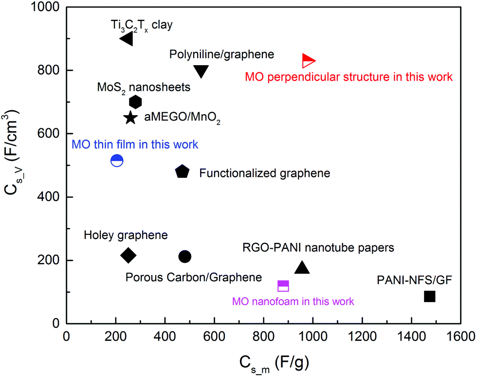 | ||
| Fig. 7 Comparison of the Cs_m and Cs_V of the MO nanostructures with other materials repoted in the literature, such as polyaniline/graphene composites,64 Ti3C2Tx clay,65 MoS2 nanosheets,66 functionalized graphene sheets,67 porous carbon layer/graphene,68 RGO-F/PANI nanotube papers,69 aMEGO/MnO2,70 PANI-NFS/GF,71 porous carbon/grapnhene composites72 and holey graphene.73 | ||
In the MO electrodes prepared by PLD with an O2 pressure of 5 Torr,41 a significant increase of Cs_m was observed during the life-cycle tests. The normal capacitance increase at the early stage of the cycles due to the activation effect78,79 cannot explain such a big change. This has been interpreted as a result of the contact improvement between nanoparticles during the charge/discharge cycles. With the four samples prepared in different O2 pressures and persisting distinct microstructures, we did further investigation on the Cs_m increase at the beginning of the life-cycle tests. The cycling test was carried out at 50 mV s−1 for 500 cycles. The CV curves for MO20 and Cs_m as a function of cycle numbers for all the samples are presented in Fig. 6. Other CV curves could be found in the ESI.† From Fig. 8(a) one could see clearly the modifications of the CV curves with the increase of the cycle numbers (indicated by the arrow in the figure). The current at a voltage higher than 0.8 V continuously decreased. On the contrary, the current between 0.2 and 0.8 V in the upper branch and between 0 and 0.6 V in the lower branch increased more significantly than the current decrease with a voltage above 0.8 V. As a result, the area in the CV curves increased with the increase of the cycle numbers. The same effect was observed in MO10 but it was much weaker. The CV curves of the other two samples, MO01 and MO05, did not show such a modification (see the ESI†).
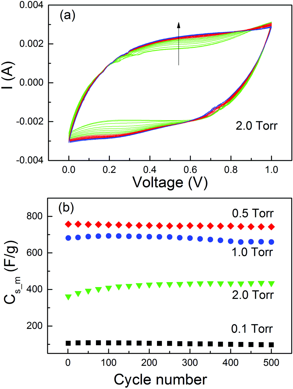 | ||
| Fig. 8 (a) Cycling stability profile for MO20 at a voltage scan rate of 50 mV s−1. The arrow indicates the increase of cycle numbers from 1 to 500. (b) Cs_m at different cycle numbers from 1 to 500 cycles. | ||
The Cs_m values obtained from the CV curves are plotted in Fig. 8(b). No Cs_m increase was observed for the samples MO01 and MO05. The Cs_m values increased by only ∼1% for MO10 from cycle 1 to cycle 200 (681 F g−1 to 689 F g−1) and by more than 18% for MO20 (from 361 F g−1 to 426 F g−1). Both of them were much smaller than that for the sample prepared in 5 Torr of O2,41 in which the Cs_m value increases by more than 100% from cycle 1 to cycle 200. The results clearly indicated that the increase of Cs_m was closely related with the morphology of the active material on the electrodes. For the thin films and perpendicular columnar structures, all MOs had good contact with the substrate and consequently, no Cs_m increase was observed. The phenomenon occurred only in the samples with foam-like microstructures. However, the percentage of increase was related to the O2 pressure during deposition, which determines the density of the MO nanofoam. The higher the pressure of the O2 atmosphere, the lower the density and weaker contact between the nanoparticles. Structural modification accompanied with the loss of conductive pathways during the i/e process induced by mechanical stress normally leads to a capacitance decrease.80 In our case, the i/e process of the ions during charge/discharge cycles induced a mechanical pressure on the active materials and such a pressure had a much stronger effect on the samples with lower density and weaker contacts. As a result, a Cs_m increase in the foam-like samples was observed. The long-term stability of the MO electrodes should be tested for up to at least 5000 cycles. However, due to the great difficulty of access to laboratories during this time, we could not perform the experiment.
4 Conclusions
In summary, we prepared MO nanostructures by PLD in different O2 pressures with a metallic Mn target. The deposition rates decreased with the increase of the O2 pressure. Different microstructures were obtained for the MO samples, from thin films to perpendicular columnar structures and eventually to extra-low density nanofoams. The prepared nanomaterials were investigated as supercapacitor electrodes. The microstructures had a great effect on supercapacitor properties. The EDLC contribution increased significantly when the nanostructures changed from thin films to nanofoams due to the increase of the specific surface area. The thin film had the lowest Cs_m value but a quite high Cs_V because of the high density. The electrode with a perpendicular columnar structure showed both high Cs_m (976 F g−1) and Cs_V and (830 F cm−3), suggesting a good choice for most of the applications of supercapacitors. The foam-like structure with extra-low densities exhibited the best performance with fast charge/discharge rates. For some special applications with respect to the high charge/discharge rates and no limitation of the volume, the MO nanofoam could be a good candidate. The life-cycle test showed that there was an activation effect for the MO nanofoams and the effect was stronger with the lower density MO nanomaterials. We concluded that the mechanical pressure induced by the ion i/e process during charge/discharge improved the contacts between the MO nanoparticles and as a result, the Cs_m increased after several cycles. The stability for more cycles still needs further investigation to study the morphology effect on the mechanical stability of the electrodes. Our results showed clearly the pure morphology effect on the supercapacitive properties of the MO nanostructures and hence might benefit the material design for supercapacitor electrodes.Conflicts of interest
There are no conflicts to declare.Acknowledgements
The authors gratefully acknowledge FAPERJ for the support with grant numbers of E-26/202.790/2015, E-26/010.000978/2019 and E-26/010.001550/2019. This study was also supported, in part, by the Coordenação de Aperfeiçoamento de Pessoal de Nível Superior – Brasil (CAPES) – Finance Code 001.Notes and references
- D. P. Dubal, O. Ayyad, V. Ruiz and P. Gómez-Romero, Chem. Soc. Rev., 2015, 44, 1777–1790 Search PubMed
.
- Z. Yu, L. Tetard, L. Zhai and J. Thomas, Energy Environ. Sci., 2015, 8, 702–730 Search PubMed
- Poonam, K. Sharma, A. Arora and S. Tripathi, J. Energy Storage, 2019, 21, 801–825 Search PubMed
- Y.-Z. Wang, X.-Y. Shan, D.-W. Wang, H.-M. Cheng and F. Li, J. Energy Chem., 2019, 38, 214–218 Search PubMed
- Z. Yang, J. Tian, Z. Yin, C. Cui, W. Qian and F. Wei, Carbon, 2019, 141, 467–480 Search PubMed
- W. Zhang, C. Xu, C. Ma, G. Li, Y. Wang, K. Zhang, F. Li, C. Liu, H.-M. Cheng, Y. Du, N. Tang and W. Ren, Adv. Mater., 2017, 29, 1701677 Search PubMed
- T. Zhu, J. Zhou, Z. Li, S. Li, W. Si and S. Zhuo, J. Mater. Chem. A, 2014, 2, 12545–12551 Search PubMed
- Z. Qiu, Y. Wang, X. Bi, T. Zhou, J. Zhou, J. Zhao, Z. Miao, W. Yi, P. Fu and S. Zhuo, J. Power Sources, 2018, 376, 82–90 Search PubMed
- G. A. Snook, P. Kao and A. S. Best, J. Power Sources, 2011, 196, 1–12 Search PubMed
- X. Wu, W. Xing, L. Zhang, S. Zhuo, J. Zhou, G. Wang and S. Qiao, Powder Technol., 2012, 224, 162–167 Search PubMed
- C. Lokhande, D. Dubal and O.-S. Joo, Curr. Appl. Phys., 2011, 11, 255–270 Search PubMed
- J. Hao, S. Peng, H. Li, S. Dang, T. Qin, Y. Wen, J. Huang, F. Ma, D. Gao, F. Li and G. Cao, J. Mater. Chem. A, 2018, 6, 16094–16100 Search PubMed
- K. S. Bhat and H. S. Nagaraja, Mater. Res. Express, 2018, 5, 105504 Search PubMed
- R. Hou, G. S. Gund, K. Qi, P. Nakhanivej, H. Liu, F. Li, B. Y. Xia and H. S. Park, Energy Storage Mater., 2019, 19, 212–241 Search PubMed
- D.-G. Wang, Z. Liang, S. Gao, C. Qu and R. Zou, Coord. Chem. Rev., 2020, 404, 213093 Search PubMed
- D. Shanbhag, K. Bindu, A. Aarathy, M. Ramesh, M. Sreejesh and H. Nagaraja, Mater. Today Energy, 2017, 4, 66–74 Search PubMed
- K. S. Bhat and H. Nagaraja, Electrochim. Acta, 2019, 302, 459–471 Search PubMed
- J. Jiang and A. Kucernak, Electrochim. Acta, 2002, 47, 2381–2386 Search PubMed
- A. González, E. Goikolea, J. A. Barrena and R. Mysyk, Renewable Sustainable Energy Rev., 2016, 58, 1189–1206 Search PubMed
- W. Wei, X. Cui, W. Chen and D. G. Ivey, Chem. Soc. Rev., 2011, 40, 1697–1721 Search PubMed
- C.-C. Hu and T.-W. Tsou, Electrochem. Commun., 2002, 4, 105–109 Search PubMed
- B. Messaoudi, S. Joiret, M. Keddam and H. Takenouti, Electrochim. Acta, 2001, 46, 2487–2498 Search PubMed
- Q.-Z. Zhang, D. Zhang, Z.-C. Miao, X.-L. Zhang and S.-L. Chou, Small, 2018, 14, 1702883 Search PubMed
- Y. Dai, K. Wang and J. Xie, Appl. Phys. Lett., 2007, 90, 104102 Search PubMed
- B. Li, X. Zhang, J. Dou and C. Hu, Ceram. Int., 2019, 45, 16297–16304 Search PubMed
- Y.-H. Son, P. T. M. Bui, H.-R. Lee, M. S. Akhtar, D. K. Shah and O.-B. Yang, Coatings, 2019, 9, 631 Search PubMed
- X. Zhao, B. M. Sánchez, P. J. Dobson and P. S. Grant, Nanoscale, 2011, 3, 839–855 Search PubMed
- M. Aghazadeh, M. Ghannadi Maragheh, M. R. Ganjali and P. Norouzi, RSC Adv., 2016, 6, 10442–10449 Search PubMed
- Y. Wang and I. Zhitomirsky, Langmuir, 2009, 25, 9684–9689 Search PubMed
- D. Yang, J. Power Sources, 2012, 198, 416–422 Search PubMed
- R. N. Reddy and R. G. Reddy, J. Power Sources, 2003, 124, 330–337 Search PubMed
- J. Jiang, J. Li, X. Long, D. Zhao, K. Su, D. Xv, C. Yang and D. Qian, Mater. Res. Bull., 2019, 109, 29–33 Search PubMed
- D. Yan, Z. Guo, G. Zhu, Z. Yu, H. Xu and A. Yu, J. Power Sources, 2012, 199, 409–412 Search PubMed
- M. Jana, S. Saha, P. Samanta, N. C. Murmu, N. H. Kim, T. Kuila and J. H. Lee, J. Power Sources, 2017, 340, 380–392 Search PubMed
- B. S. Singu, S. E. Hong and K. R. Yoon, J. Energy Storage, 2019, 25, 100851 Search PubMed
- Y. Wang, C. Chen, X. Ding, L. Chu, Z. Deng, W. Liang, J. Chen and G. Fu, Laser Part. Beams, 2011, 29, 105–111 Search PubMed
- H. Luna, D. F. Franceschini, R. Prioli, R. B. Guimarães, C. M. Sanchez, G. P. Canal, M. D. L. Barbosa and R. M. O. Galvão, J. Vac. Sci. Technol., A, 2010, 28, 1092–1098 Search PubMed
- F. Fabris, Y. T. Xing, D. F. Franceschini, D. R. Sanchez, M. Alzamora and W. C. Nunes, J. Appl. Phys., 2017, 122, 063901 Search PubMed
- S. Isber, E. Majdalani, M. Tabbal, T. Christidis, K. Zahraman and B. Nsouli, Thin Solid Films, 2009, 517, 1592–1595 Search PubMed
- C.-C. Hu, C.-Y. Hung, K.-H. Chang and Y.-L. Yang, J. Power Sources, 2011, 196, 847–850 Search PubMed
- J. N. Lacerda, D. F. Franceschini, E. A. Ponzio, L. M. Esteves, R. B. Guimaraes and Y. T. Xing, Mater. Chem. Phys., 2020, 242, 122459 Search PubMed
- H. Wang, Y. Wang and X. Wang, New J. Chem., 2013, 37, 869–872 Search PubMed
- D. Yang, J. Power Sources, 2011, 196, 8843–8849 Search PubMed
- A. Rode, E. Gamaly and B. Luther-Davies, Appl. Phys. A: Mater. Sci. Process., 2000, 70, 135 Search PubMed
- A. Zani, D. Dellasega, V. Russo and M. Passoni, Carbon, 2013, 56, 358–365 Search PubMed
- G. Atanasova, A. O. Dikovska, T. Dilova, B. Georgieva, G. Avdeev, P. Stefanov and N. Nedyalkov, Appl. Surf. Sci., 2019, 470, 861–869 Search PubMed
- H. Li, C. Qi, Y. Tao, H. Liu, D.-W. Wang, F. Li, Q.-H. Yang and H.-M. Cheng, Adv. Energy Mater., 2019, 9, 1900079 Search PubMed
- Z. Li, S. Gadipelli, H. Li, C. A. Howard, D. J. L. Brett, P. R. Shearing, Z. Guo, I. P. Parkin and F. Li, Nat. Energy, 2020, 5, 160–168 Search PubMed
- J. Avila-Avendano, I. Mejia, H. N. Alshareef, Z. Guo, C. Young and M. Quevedo-Lopez, Thin Solid Films, 2016, 608, 1–7 Search PubMed
- N. R. C. Raju, K. J. Kumar and A. Subrahmanyam, J. Phys. D: Appl. Phys., 2009, 42, 135411 Search PubMed
- J. N. Zeng, J. K. Low, Z. M. Ren, T. Liew and Y. F. Lu, Appl. Surf. Sci., 2002, 197–198, 362–367 Search PubMed
- M. Ghidelli, L. Mascaretti, B. R. Bricchi, A. Zapelli, V. Russo, C. S. Casari and A. L. Bassi, Appl. Surf. Sci., 2018, 434, 1064–1073 Search PubMed
-
H.-U. Krebs, M. Weisheit, J. Faupel, E. Süske, T. Scharf, C. Fuhse, M. Störmer, K. Sturm, M. Seibt, H. Kijewski, D. Nelke, E. Panchenko and M. Buback, Advances in Solid State Physics, Springer Berlin Heidelberg, Berlin, Heidelberg, 2003, pp. 505–518 Search PubMed
- T. Gao, H. FjellvÅg and P. Norby, Anal. Chim. Acta, 2009, 648, 235–239 Search PubMed
- X. Gu, J. Yue, L. Li, H. Xue, J. Yang and X. Zhao, Electrochim. Acta, 2015, 184, 250–256 Search PubMed
- R. Tholkappiyan, A. N. Naveen, K. Vishista and F. Hamed, J. Taibah Univ. Sci., 2018, 12, 669–677 Search PubMed
- S. Ardizzone, G. Fregonara and S. Trasatti, Electrochim. Acta, 1990, 35, 263–267 Search PubMed
- Y.-H. Lee, K.-H. Chang and C.-C. Hu, J. Power Sources, 2013, 227, 300–308 Search PubMed
- J. Duay, S. A. Sherrill, Z. Gui, E. Gillette and S. B. Lee, ACS Nano, 2013, 7, 1200–1214 Search PubMed
- J. Wang, J. Polleux, J. Lim and B. Dunn, J. Phys. Chem. C, 2007, 111, 14925–14931 Search PubMed
- C. Liu, E. I. Gillette, X. Chen, A. J. Pearse, A. C. Kozen, M. A. Schroeder, K. E. Gregorczyk, S. B. Lee and G. W. Rubloff, Nat. Nanotechnol., 2014, 9, 1031–1039 Search PubMed
- C. Sun, Y. Zhang, S. Song and D. Xue, J. Appl. Crystallogr., 2013, 46, 1128–1135 Search PubMed
- H. Li, X. Zhang, R. Ding, L. Qi and H. Wang, Electrochim. Acta, 2013, 108, 497–505 Search PubMed
- Y. Xu, Y. Tao, X. Zheng, H. Ma, J. Luo, F. Kang and Q.-H. Yang, Adv. Mater., 2015, 27, 8082–8087 Search PubMed
- M. Ghidiu, M. R. Lukatskaya, M.-Q. Zhao, Y. Gogotsi and M. W. Barsoum, Nature, 2014, 516, 78–81 Search PubMed
- M. Acerce, D. Voiry and M. Chhowalla, Nat. Nanotechnol., 2015, 10, 313–318 Search PubMed
- J. Yan, Q. Wang, T. Wei, L. Jiang, M. Zhang, X. Jing and Z. Fan, ACS Nano, 2014, 8, 4720–4729 Search PubMed
- J. Yan, Q. Wang, T. Wei and Z. Fan, Adv. Energy Mater., 2014, 4, 1300816 Search PubMed
- C. Yang, L. Zhang, N. Hu, Z. Yang, Y. Su, S. Xu, M. Li, L. Yao, M. Hong and Y. Zhang, Chem. Eng. J., 2017, 309, 89–97 Search PubMed
- X. Zhao, L. Zhang, S. Murali, M. D. Stoller, Q. Zhang, Y. Zhu and R. S. Ruoff, ACS Nano, 2012, 6, 5404–5412 Search PubMed
- J. Pedrós, A. Boscá, J. Martínez, S. Ruiz-Gómez, L. Pérez, V. Barranco and F. Calle, J. Power Sources, 2016, 317, 35–42 Search PubMed
- J. Yan, Q. Wang, C. Lin, T. Wei and Z. Fan, Adv. Energy Mater., 2014, 4, 1400500 Search PubMed
- L. Yan, D. Li, T. Yan, G. Chen, L. Shi, Z. An and D. Zhang, ACS Sustainable Chem. Eng., 2018, 6, 5265–5272 Search PubMed
- A. Teli, S. Bekanalkar, D. Patil, S. Pawar, T. Dongale, J. Shin, H. Kim and P. Patil, J. Electroanal. Chem., 2020, 856, 113483 Search PubMed
- A. M. Teli, S. A. Beknalkar, D. S. Patil, S. A. Pawar, D. P. Dubal, V. Y. Burute, T. D. Dongale, J. C. Shin and P. S. Patil, Appl. Surf. Sci., 2020, 511, 145466 Search PubMed
- V. Mane, D. Malavekar, S. Ubale, R. Bulakhe, I. In and C. Lokhande, Electrochim. Acta, 2020, 335, 135613 Search PubMed
- Y. Tian, C. Yang, W. Que, X. Liu, X. Yin and L. B. Kong, J. Power Sources, 2017, 359, 332–339 Search PubMed
- Y.-H. Lin, T.-Y. Wei, H.-C. Chien and S.-Y. Lu, Adv. Energy Mater., 2011, 1, 901–907 Search PubMed
- Y. Wu, S. Liu, H. Wang, X. Wang, X. Zhang and G. Jin, Electrochim. Acta, 2013, 90, 210–218 Search PubMed
- E. A. Ponzio, T. M. Benedetti and R. M. Torresi, Electrochim. Acta, 2007, 52, 4419–4427 Search PubMed
Footnote |
| † Electronic supplementary information (ESI) available: Deposition conditions and other parameters for the MO nanostructures, XPS survey spectra and fitting results of the O spectra, cyclic voltammetry and cycling stability profile of other samples and calculations of capacitive contribution. See DOI: 10.1039/d0ma00524j |
| This journal is © The Royal Society of Chemistry 2020 |