DOI:
10.1039/D0MA00554A
(Paper)
Mater. Adv., 2020,
1, 2426-2432
Nitrogen doping-induced local structure change in a Cr2Ge2Te6 inverse resistance phase-change material†
Received
30th July 2020
, Accepted 28th August 2020
First published on 2nd September 2020
Abstract
Fast and reversible switching utilizing the resistance contrast upon phase transition of phase change materials (PCMs) has been widely studied for next generation nonvolatile memory (NVM). Cr2Ge2Te6 (CrGT) and N-doped CrGT (NCrGT) PCMs have been demonstrated to show enhanced memory performance compared to the traditional Ge2Sb2Te5 (GST) PCM. We investigated here the crystallization behavior of Cr2Ge2Te6 (CrGT) and the effect of nitrogen (N) doping on it. We revealed that the Ge- or Cr-centered defective octahedral structure dominated in the amorphous phase of CrGT and the evolution of the c-axis-aligned Ge–Ge dimer and Cr-centered octahedral structure marked the beginning of crystallization. The further formation of new Cr–Te bonds resulted in a dramatic decline of carrier density in the crystalline phase, which explained the inverse resistance change between the amorphous and crystalline phases of CrGT. The N atom can form stronger bonds with Ge or Cr than Cr–Te, restraining the shift of Cr to the center of the octahedron to form the new Cr–Te bonds, resulting in a constant carrier density change during crystallization. The thermal stability and data retention properties also show an improvement by N doping.
1. Introduction
Phase-change materials (PCMs) exhibiting fast reversible electrical property changes between amorphous and crystalline phases have been attracting much attention for their application potential in non-volatile memory like phase-change random access memory (PCRAM).1–3 Traditional PCMs, such as Ge2Sb2Te5 (GST), with conspicuous advantages like a high phase transition speed and good repeatability, have been widely studied.4–6 However, some limitations still remain for the further application of PCRAM, such as the high operation energy and the poor data retention properties.7 For decades, many efforts have been made to improve the performance of PCRAM, and adding dopants into PCMs is considered as one of the most effective ways in this regard.8 Usually, traditional PCMs show much lower crystalline resistance than amorphous resistance due to the shift of the Fermi level toward the valence band tuned by excess vacancies.9,10 In contrast to traditional PCMs, a new PCM, Cr2Ge2Te6 (CrGT), exhibits inverse electrical property changes upon phase transition and shows an extremely high crystalline resistance.11 Because of the higher crystalline resistance of CrGT, it was shown to be less heat consuming and to operate at a higher speed, which are preferable performance characteristics over those of the mature GST PCM.11–14 Besides, (nitrogen) N-doped CrGT (NCrGT) with a N content of 6.5 at% has also been investigated, and it showed no resistance change during phase transformation.15 However, the NCrGT-based PCRAM cell can still achieve a typical threshold switching with a three-orders-of-magnitude resistance contrast, which can be attributed to an interfacial property difference (i.e., contact resistance contrast) between the amorphous NCrGT/electrode contact and crystalline NCrGT/electrode contact.15,16 Both CrGT and NCrGT are qualified alternatives to GST, presenting a higher crystallization temperature (Tx) and larger activation energy, and hence a higher amorphous thermal stability against thermal crosstalk in high-density memory cell arrays.14 Especially, NCrGT shows a higher crystallization temperature (Tx) at around 300 °C, endowing it with high potential to be applied in a high-temperature environment. In addition, this non-bulk NCrGT-based PCRAM resistance change can realize self-selected performance with the introduction of an n-type oxide semiconductor layer.16 However, these unique phase-change behaviors of the pure CrGT and NCrGT PCMs and their structure evolution details are still in question, making their better understanding and utilization a challenge, particularly for amorphous PCMs due to the lack of long-range correlations. The role of the N dopant in the CrGT matrix is still not fully understood.
Raman scattering (RS) is a powerful tool to study the structure of both amorphous and crystalline materials. In recent years, many authors have achieved significant progress in studying the structure of PCMs by employing RS. Andrikopoulos et al. reported a possible model of the atomic configuration of GeTe during phase transition with the aid of RS spectroscopy.17 Li et al. revealed that carbon doping can reduce the portion of the tetrahedral unit of Ge–Te in an amorphous GST via RS.18 Park et al. also demonstrated the role of intermediate Ge–Te bonding in the crystallization mechanism by applying RS spectroscopy in laser irradiation-modified amorphous phase GeTe.19 In this study, we show the possible CrGT phase transition evolution and N integration effect based on the results of RS analysis, combined with the results obtained from X-ray diffraction (XRD). Via RS spectroscopy, we revealed that the amorphous CrGT firstly crystallized to a metastable state at a lower temperature; in the metastable state, we observed a long-range order structure of CrGT, while some local bonding configuration that is similar to amorphous structures such as Cr–Te local pieces still remained. The further formation of new Ge–Ge and Cr–Te bonds in the octahedral structure is the key process for the transition from the metastable crystalline state with a high carrier density to a stable state with a low carrier density. The N atom plays a paramount role in the transformation of local configuration, resulting in a suppression of crystal growth. We verified a high thermal stability and good data retention property, which are attributed to the N atom inducing the enhancement of activation energy for crystallization.
2. Experimental
We deposited CrGT and NCrGT films (100 nm) studied in this work on SiO2 (100 nm)/Si substrates by radio frequency (RF) magnetron co-sputtering of Ge (3N), Cr (4N), and Te (4N) targets at room temperature. The base pressure was less than 5 × 10⁻⁵ Pa. We adjusted the RF power of each target to obtain a near-stoichiometric Cr2Ge2Te6 composition. Argon (Ar) gas flow rate was 15 sccm (sccm denotes cubic centimeter per minute at standard pressure and temperature), and the working pressure was around 0.35 Pa. During the deposition, we basically controlled the N gas flow rate to be 0.4 SCCM, where the N gas flow rate caused an integration of 6.5 at% N in the CrGT film (NCrGT), verified via X-ray photoelectron spectroscopy (XPS, Thermo VG, Theta Probe). We also performed XPS measurements to analyze the chemical bonding state of the elements in the as-deposited CrGT and NCrGT films. Ar ion etching for 570 s with a 2 kV ion gun was carried out to remove the surface oxidation layer before the XPS measurements. All energies were calibrated with the C 1s peak at 285.0 eV. We then annealed the films at various temperatures in a heating furnace equipped with a two-point probe measurement system in an Ar gas atmosphere; the heating rate was 10 °C min−1. We measured the resistance of the films as a function of temperature (R–T) using the two-point probe system with tungsten (W) electrode probes. We studied the crystal structure of the as-deposited and annealed films using XRD (Rigaku, Ultima IV); the diffraction patterns were recorded in the 2θ range of 10°–60°, with Cu Kα radiation. We recorded the RS spectra using a micro-Raman spectrometer (NRS-5500) with an incident wavelength of 532 nm. We capped all the samples in the RS measurement with a 50 nm SiO2 protection layer to avoid surface oxidation. We set the laser power as 0.1 mW to avoid unwanted phase transition or possible damage by laser irradiation. The accumulation time of each spectrum was 30 s with 30 cycles. By measuring the Si standard sample, we performed wavenumber calibration. By co-sputtering, we deposited a GeTe thin film with a stoichiometric composition of 1![[thin space (1/6-em)]](https://www.rsc.org/images/entities/char_2009.gif) :1 and CrTex thin films with various compositions from x = 1.5 to x = 3 as reference samples for the RS spectral analysis, respectively. We confirmed all the as-deposited GeTe and CrTex thin films as amorphous phases using XRD, and the thicknesses of the films were around 100 nm (Fig. S1(a), ESI†). We measured the electrical properties of CrGT and NCrGT at room temperature using a Hall effect measurement instrument (Toyo Corporation, ResiTest 8400) with the AC measurement mode. We deposited all the thin films prepared for Hall effect measurement on a glass substrate. To evaluate the data retention properties of amorphous NCrGT films at varying heating rates of 10–50 °C min−1 in an Ar atmosphere, we performed non-isothermal differential scanning calorimetry (DSC) (TA Instruments, Q20).
:1 and CrTex thin films with various compositions from x = 1.5 to x = 3 as reference samples for the RS spectral analysis, respectively. We confirmed all the as-deposited GeTe and CrTex thin films as amorphous phases using XRD, and the thicknesses of the films were around 100 nm (Fig. S1(a), ESI†). We measured the electrical properties of CrGT and NCrGT at room temperature using a Hall effect measurement instrument (Toyo Corporation, ResiTest 8400) with the AC measurement mode. We deposited all the thin films prepared for Hall effect measurement on a glass substrate. To evaluate the data retention properties of amorphous NCrGT films at varying heating rates of 10–50 °C min−1 in an Ar atmosphere, we performed non-isothermal differential scanning calorimetry (DSC) (TA Instruments, Q20).
3. Results and discussion
3.1. Crystallization of CrGT and NCrGT
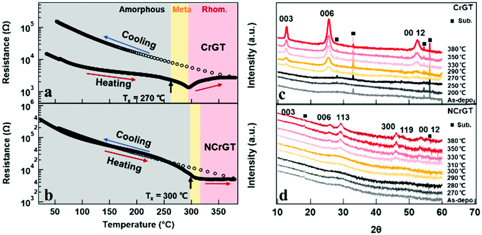
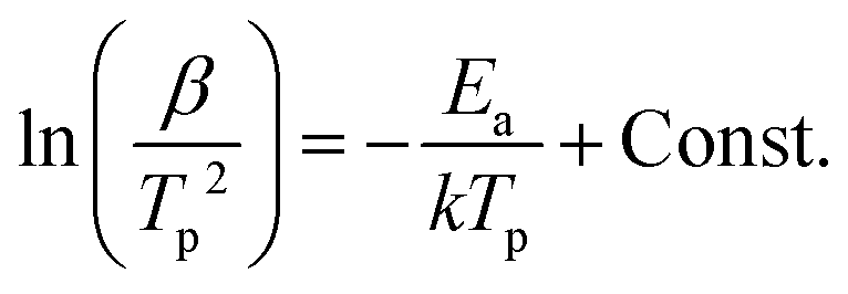
Fig. 1(a) and (b) show the in situ temperature-dependent resistance (R–T) curves of CrGT and NCrGT, respectively. Fig. 1(c) and (d) show the XRD patterns obtained at room temperature for the CrGT and NCrGT films annealed up to the expected temperature, respectively. We confirmed that both the as-deposited films show an amorphous phase. The resistances of both the as-deposited amorphous films decreased with increasing temperature, indicating a semiconductor-like property. Some Bragg reflection peaks derived from a crystalline phase in the XRD pattern of the pure CrGT appeared at 270 °C, which indicated the beginning of crystallization, while in the NCrGT film, reflection peaks clearly appeared at more than 310 °C, which suggested that N doping could improve the thermal stability of the amorphous CrGT phase (Fig. 1(d)). The crystal structure of both films will be mentioned later. Combining the results of the R–T and XRD measurements, we determined the Txs of the pure CrGT and NCrGT films to be about 270 °C and 300 °C, respectively, which is consistent with a previous work.15 The reflection peaks become sharper with increasing temperature, indicating that the grain size keeps increasing with increasing temperature. Unlike the traditional PCMs, the pure CrGT shows a decrease in resistance just after Tx and then keeps increasing after 290 °C, while NCrGT shows a slight resistance decline and then maintains a constant resistance change after Tx.11,15 After heating the films to 380 °C, we furnace-cooled them to room temperature. For both films, in the cooling process, the resistance continuously increased with decreasing temperature. Consequently, the pure CrGT film exhibited an increase in resistance by about one order of magnitude upon crystallization, while almost no resistance contrast existed in the NCrGT film even after the crystallization.
 |
| | Fig. 1
R–T curves of (a) pure CrGT and (b) NCrGT; the films were annealed up to 380 °C followed by furnace-cooling to room temperature. XRD patterns at room temperature for (c) pure CrGT and (d) NCrGT films annealed up to the expected temperature (the temperature indicated at the right side of each XRD pattern). | |
The higher crystalline resistance in CrGT, which differs from that in traditional PCMs, is suggested to originate from the unique bonding configuration. The addition of a transition metal (TM) to PCMs is one of the ways to induce a large local structure change of PCMs. Wang et al. have studied the effects of Cr addition on the atomic arrangement of traditional GST by aberration-corrected scanning transmission electron microscopy (STEM) and they revealed Te–Cr–Te layers enclosed by Ge/Sb–Te bilayer structures.20 The results indicate that the Cr atoms prefer to occupy the octahedral site in the hexagonally close packed structure of Te anions. In our CrGT PCM, Cr atoms are also involved in the octahedral sites, while only two-thirds of the octahedrons can be occupied in each layer with the other one-third filled by Ge–Ge dimers.21,22 The crystal structure of the CrGT compound is shown in Fig. S2 (ESI†). Various types of bonds are found to exist in CrGT including Cr–Te ionic bonding, Ge–Te covalent bonding, etc., which is distinct from the covalent bonding dominant in traditional PCMs.21 The noticeable difference of atomic arrangement and the bonding type between the crystalline CrGT and Cr-doped GST PCMs gives rise to distinct electrical properties. The pure CrGT film shows the Bragg reflection peaks derived from 003, 006, and 0012 of the CrGT crystal plane after crystallization at a temperature higher than 270 °C, revealing c-axis preferential crystal growth. Meanwhile, the reflection peaks in the crystalized NCrGT film were weaker and broader due to grain size refinement by N doping. In addition, in the NCrGT film, the peak positions of 003, 006, and 0012 shift toward a higher angle, which represents shrinkage of the out-of-plane lattice spacing along the c-direction. The shrinkage may be due to the substitution of Ge, Cr, or Te atoms by the smaller atomic radius N atom. The XRD patterns of the NCrGT films have other reflection peaks, which are also indexed as the rhombohedral structure of CrGT. The appearance of the XRD peaks from other planes indicates that the N dopant can inhibit the out-of-plane c-axis oriented growth of the CrGT thin films during the annealing process.
3.2. Local structures in amorphous CrGT and NCrGT
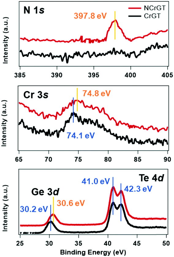
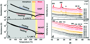
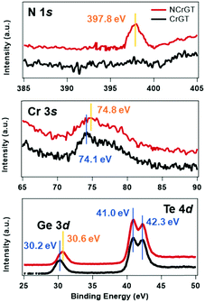
The amorphous structure is key to understanding the phase-change mechanism. However, it is difficult to extract information from the XRD patterns since we observed no peak from XRD. Here, we have measured the RS spectra of the as-deposited amorphous phase of CrGT and NCrGT, which showed obvious peaks within the range of 50–250 cm−1 (Fig. 2(a) and (b)). Since the phonon lifetime of a disordered material is a random distribution, as opposed to a finite value in a crystalline material, the peak shape of the Raman mode can be described by a Gaussian line fitting procedure.19 To obtain a good baseline without a larger error, we conducted a smoothing process for the raw data prior to the fitting procedure (Fig. 2). Table 1 summarizes the fitting results of CrGT and NCrGT. Both the as-deposited films have similar RS spectra, suggesting that there is no dramatic change taking place in the amorphous CrGT matrix by N doping. Since there is no complete crystal structure in the amorphous phase, the main bonding configuration might consist of Ge–Ge, Ge–Te, Te–Te, and Cr–Te according to the crystalline CrGT bonding configuration. So, we can capture some pieces of the local structure by comparing it with the reference samples such as amorphous GeTe and CrTe binary compounds. Fig. 2(d) presents the typical Raman active modes for the as-deposited amorphous GeTe film. The spectrum is deconvolved into five principle Gaussian contributions, denoted as A1 (82.71 cm−1), A2 (92.58 cm−1), B (115.18 cm−1), C (156.80 cm−1), and D (209.90 cm−1) in the frequency range of 50–250 cm−1, which is consistent with the reported Raman bands.17,23,24 The Raman spectrum and peak assignment of amorphous GeTe have been widely studied by many researchers. The peaks A1 and A2 can be ascribed to the three-fold coordinated Te atoms. Andrikopoulos et al. suggested that the sp3 valence electrons of Ge atoms can be saturated in the form of a GeTe4−nGen tetrahedral geometry, so the Raman active modes of GeTe in peaks B and C originate from the stretching modes of tetrahedral Ge atoms.17 However, Kolobov et al. confirmed from extended X-ray absorption fine structure (EXAFS) study that the coordination number of the Ge atom is less than 4; therefore, octahedral-like 3(Ge):3(Te) and tetrahedral 4(Ge):2(Te) should coexist in as-deposited amorphous GeTe, and peaks B and C are associated with the vibrations of Ge atoms in a defective octahedral site with three shorter bonds.19,25,26 Peak D can be assigned to a vibration mode of a Ge-richer GeTe4−nGen tetrahedral geometry.27 In a previous EXAFS study of an as-deposited amorphous CrGT, the Ge–Te and Ge–Ge bond lengths were found to be 2.65 and 2.48 Å, respectively, which is similar to the cases of GeTe or GST, and suggests a covalent bonding nature of CrGT. The total coordination numbers of Ge and Te in the as-deposited amorphous CrGT film were determined to be 2.7 and 2.9, respectively.12 Thus, the local bonding configuration of the as-deposited amorphous CrGT resembles that of the as-deposited amorphous GeTe. Furthermore, five bands could be deconvolved for the Raman spectrum of CrGT with the Raman shift close to that of the as-deposited amorphous GeTe film, enhancing the similarity of the amorphous local configuration between the amorphous CrGT and GeTe films. Therefore, to identify the Raman vibration modes of the as-deposited amorphous CrGT, we can use the analogy of the Raman vibration modes between the as-deposited amorphous GeTe and CrGT thin films. The main peaks, B and C, are mainly contributed by the stretching and bending modes of a Ge-centered defective octahedral structure similar to that of GeTe, as shown in the schematic atomic structure in Fig. 2(f). A slight redshift of peak B in the as-deposited amorphous CrGT (120.28 cm−1) and NCrGT (119.38 cm−1) compared with that of GeTe (115.18 cm−1) could be observed due to the lower Ge/Te atomic ratio of CrGT.28 Moreover, it is different for GeTe, in which the intensity of peak C in the amorphous CrGT is stronger and almost equivalent with that of peak B. The higher intensity of peak C in the amorphous CrGT and NCrGT films could be due to the contribution from the Cr–Te local structure configurations. Since there are almost no reports related to amorphous Cr–Te structures, we deposited amorphous CrTex thin films at various compositions from x = 1.5 to x = 3 for Raman measurements. As can be seen from Fig. 2(e), a clear and strong peak around 154.5 cm−1 was obtained from the as-deposited amorphous CrTe3 film and the same peak also existed at larger composition ratios of Cr/Te, which further explains the higher intensity of peak C (Fig. S2(b), ESI†). Since the Cr coordination number is around 3 in the as-deposited amorphous CrGT,12 it can possibly form the same defective octahedral structure with three strong covalent bonds, see Fig. 2(f). In the as-deposited amorphous NCrGT, the intensity of peak C declined, compared with that of peak B, since more stable Cr–N or Ge–N bonds can be formed due to the larger electronegativity of N than Te atoms (Fig. 2b). So, Te atoms were assumed to be replaced by N atoms in the unit of the defective octahedron. To verify this assumption, we performed XPS measurements on both the as-deposited CrGT and NCrGT thin films. The XPS spectra of N 1s, Cr 3s, Ge 3d and Te 4d peaks are shown in Fig. 3. The N 1s core level spectra show only one peak located at 397.8 eV for NCrGT, while no peak can be seen for CrGT. The binding energy at 397.8 eV can be assigned to the typical binding energy for nitrides.29 The positions of Cr 3s and Ge 3d peaks shift to a higher binding energy with N doping, which is attributed to the presence of the Cr–N and Ge–N bonds. However, the position and shape of the Te 4d peaks do not change upon introducing N, which means that negligible Te–N bonds exist in the NCrGT film. The result is consistent with the above analysis that N dopant atoms tend to substitute the Te atoms, which also corresponds to the peak shift of XRD. Fig. 2(g) displays the possible position of N-doped atoms. By annealing up to 290 °C, the intensity of peak C in the NCrGT film kept decreasing due to the stabilization of nitride bonding (Fig. 2(c)).
 |
| | Fig. 2 Raman spectra of amorphous (a) as-deposited CrGT, (b) as-deposited NCrGT, (c) 290 °C-annealed NCrGT, (d) as-deposited GeTe, and (e) as-deposited CrTe3 films with corresponding Gaussian fitting. The schematic local structures of the as-deposited amorphous (f) CrGT and (g) NCrGT. | |
Table 1 Raman spectra of amorphous GeTe, CrTe, CrGT, and NCrGT
| Raman shift (cm−1) |
A1 |
A2 |
B |
C |
D |
| As-deposited CrGT |
80.89 |
95 |
120.28 |
154.97 |
201.26 |
| As-deposited NCrGT |
80.70 |
92.30 |
119.38 |
154.88 |
204.83 |
| 290 °C NCrGT |
80.95 |
93.06 |
123.01 |
155.76 |
204.10 |
| As-deposited GeTe |
82.71 |
91.58 |
115.18 |
156.80 |
206.90 |
| As-deposited CrTe3 |
— |
— |
— |
154.50 |
226.79 |
 |
| | Fig. 3 XPS spectra of N 1s, Cr 3s, Ge 3d and Te 4d peaks in the as-deposited amorphous CrGT and NCrGT. | |
3.3. Local structures of CrGT and NCrGT in the crystallization process
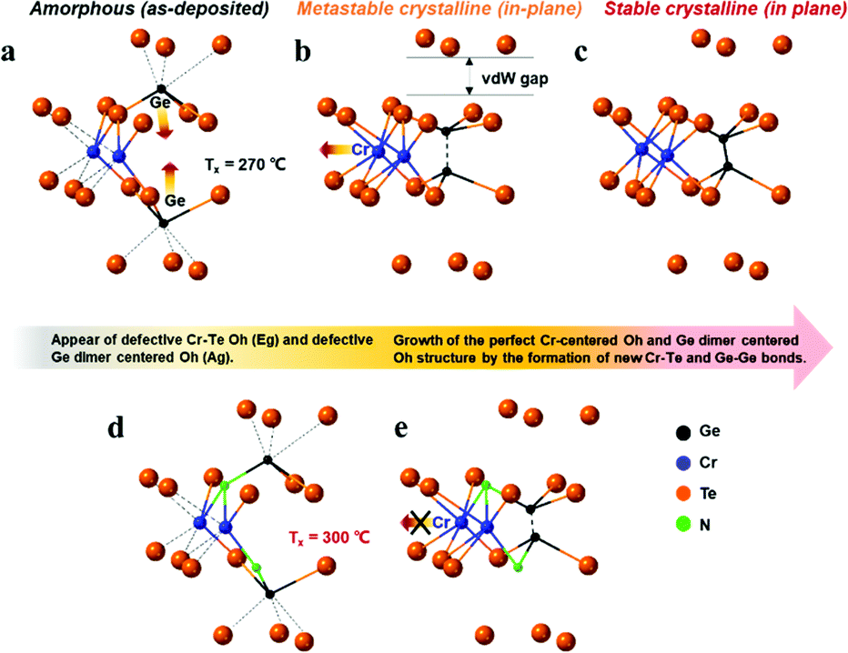
Fig. 4(a) and (b) show the Raman spectra for the pure CrGT and NCrGT films annealed up to the expected temperature, respectively. The Raman spectra of the pure CrGT film exhibited six obvious variations upon crystallization with increasing temperature—Raman modes at 82, 107, 133, 209, 230, and 291 cm−1 appeared. The NCrGT film also exhibited a similar behavior in the Raman spectral variations upon crystallization. Several researchers have extensively studied the Raman spectrum of crystalline CrGT based on group theory.30 The six modes located at 82, 107, 133, 209, 230, and 291 cm−1 are Eg1, Eg2, Ag1, Eg3, Eg4, and Ag2, respectively.30 Sun et al. calculated the vibration patterns of two main peaks, the Eg2 and Ag1 Raman active modes, to comprehend the relationship between Raman mode and the crystal structure.31 The Eg2 mode involves the twisting vibration of Cr or Ge octahedral pieces and shear vibration of Ge atoms, while the Ag1 mode involves the stretching vibration of the Ge–Ge bonds. We then discuss the possible phase evolution mechanism based on the Raman vibration mode (Fig. 5). The amorphous CrGT started to crystallize at around 270 °C, where the Raman peaks A1 and A2 of the amorphous CrGT evolved into the crystalline CrGT vibration mode of Eg1, and peak D evolved into Eg3 and Eg4 without a large change of peak intensity or position upon crystallization. However, the main peaks, B and C, in CrGT were dramatically modified upon crystallization; this should be the key evidence for the phase-change mechanism of CrGT and NCrGT. Peak B converted to the vibration modes of Ag1 and Eg2, suggesting the formation of new Ge–Ge bonds along the c-axis and the Cr-centered octahedral structure with long-range order12 (Fig. 5(a) and (b)). Here, the formation mechanism of Ge–Ge bonding from the distorted octahedron has been successfully demonstrated by a Ge flipping model.32,33 Notably, peak C still exists in the 270 °C-annealed sample, indicating that some amorphous local structures still remained (Fig. 4(a)). A previous study has already demonstrated that Te atoms can form an octahedral configuration at the beginning stage of crystallization, while the Cr atom does not reside at the center of the octahedral configuration at this stage as the coordination number of Cr is still around 3.12 The 270 °C-annealed CrGT with long-range atomic order and lingering local amorphous structure can be regarded as a metastable phase. Therefore, the lingering peak C is possibly attributed to the Cr–Te local structure and it diminishes with the shift of the Cr atom to the center of the Te octahedron, causing the reconfiguration of new Cr–Te bonds with further annealing at a higher temperature (Fig. 5(c)). The NCrGT film started to crystallize at 300 °C with only the Ag1 mode, indicating that the formation of the Te octahedron is caused by N replacement (Fig. 5 (d)). The Eg2 mode appeared above 310 °C and kept growing with further heating. Peak C in the as-deposited amorphous NCrGT film did not disappear even after sufficient crystallization, suggesting that the stronger binding energy of Cr–N suppressed the shift of Cr atoms to the center of the octahedral site, and the distorted metastable structure remained (Fig. 5(e)). This metastable structure might accelerate the phase transition speed during the device switching due to its local structure similarity with the amorphous phase.
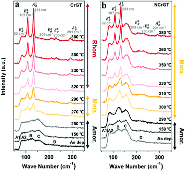 |
| | Fig. 4 Raman spectra at room temperature for (a) pure CrGT and (b) NCrGT films annealed up to various temperatures. | |
 |
| | Fig. 5 Possible phase evolution mechanism of (a)–(c) CrGT and (d) and (e) NCrGT; the dotted lines indicate the distorted bonds. | |
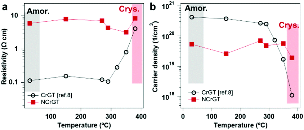
We can also explain the unique change of resistance upon crystallization. Fig. 6(a) shows a dramatic increment of resistivity in CrGT after crystallization and an almost constant resistivity in NCrGT upon crystallization. The increment of the resistance in the crystalline CrGT was already confirmed to be related to the gradual filling of Cr vacancies in the amorphous phase.11 The decline of Cr vacancies resulted in a reduction of the carrier density by two orders, while in NCrGT, the existence of Cr–N bonds restrained the occupation of Cr vacancies upon crystallization; consequently, the carrier density kept constant in both phases, and the NCrGT films exhibited almost no resistance change (Fig. 6(b)).
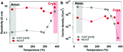 |
| | Fig. 6 (a) Resistivity and (b) carrier density of CrGT11 and NCrGT as functions of annealing temperature. | |
3.4. Thermal stability of the amorphous NCrGT film
The thermal stability of NCrGT has been further investigated using the Kissinger method34 given as:| | 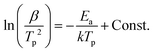 | (1) |
where peak temperature (Tp) of the NCrGT film at a heating rate β of 10, 20, 30, and 40 °C min−1 is determined from the DSC exothermic peaks (Fig. S3, ESI†). k is the Boltzmann constant and Const. is a constant. The Kissinger plots are shown in Fig. 7(a) with a linear fitting. The activation energy Ea estimated from the slope of the fit is 4.35 eV higher than that of pure CrGT (3.43 eV),11 indicating the better thermal stability of NCrGT. This higher Ea originates from the enhancement of local amorphous structure by N doping. The Ozawa method35,36 was then applied to estimate the data retention property of NCrGT by using the crystallization Ea of 4.35 eV (for detailed calculations of the Ozawa method, see Fig. S3, ESI†). The failure time vs. given temperature curve can be plotted, as shown in Fig. 7(b). The temperature corresponding to a 10 year data retention is 219 °C for NCrGT, exhibiting an excellent data retention property compared to CrGT (173 °C)11 and GST (∼80 °C),37 hence it has potential to be applied in a high-temperature environment, such as automotive applications.
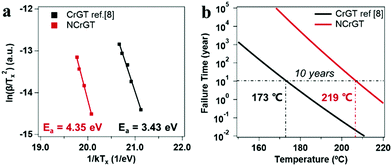 |
| | Fig. 7 (a) Kissinger plots for the activation energy calculation of the CrGT and NCrGT films and (b) temperature-dependence of failure time te 10% for the GCT and GST films. | |
4. Conclusions
In conclusion, we investigated the crystallization mechanism of CrGT and the influence of doping N on the local structure of CrGT. Raman results indicate that the structure evolution upon CrGT crystallization mainly originates from the formation of c-axis-aligned Ge–Ge dimer and Cr-centered octahedral structures. The intensity decline of the amorphous CrGT Raman peak at ∼155 cm−1 upon N doping suggests a reduction of the defective octahedral configuration due to the generation of stronger Cr–N or Ge–N bonds. The altered amorphous local structure of CrGT upon N doping results in inhibition of crystallization, which still remained even after sufficient crystallization. The activation energy of crystallization for NCrGT was calculated by the Kissinger plot to be 4.35 eV, which indicated a much better thermal stability upon N doping. The temperature corresponding to a 10 year data retention is around 219 °C for NCrGT, suggesting a possibility of application in a high-temperature environment. The understanding of the phase-change mechanism of CrGT and its N doping effect will be beneficial for further tuning of resistivity change behavior of unique CrGT PCMs by doping and the utilization of CrGT and NCrGT in PCRAM applications.
Conflicts of interest
There are no conflicts to declare.
Acknowledgements
This work was supported by KAKENHI (grant no. 19J21116, and 18H02053) and was also supported by a project, JPNP14004, subsidized by the New Energy and Industrial Technology Development Organization (NEDO).
Notes and references
- H.-S. P. Wong, S. Raoux, S. Kim, J. Liang, J. P. Reifenberg, B. Rajendran, M. Asheghi and K. E. Goodson, Proc. IEEE, 2010, 98, 2201–2227 Search PubMed.
- S. Raoux, W. Wełnic and D. Ielmini, Chem. Rev., 2010, 110, 240–267 Search PubMed.
- M. Wuttig and S. Raoux, Zeitschrift für Anorg. und Allg. Chemie, 2012, 638, 2455–2465 Search PubMed.
- J.-B. Park, G.-S. Park, H.-S. Baik, J.-H. Lee, H. Jeong and K. Kim, J. Electrochem. Soc., 2007, 154, H139 Search PubMed.
- M. Wuttig and N. Yamada, Nat. Mater., 2007, 6, 824–832 Search PubMed.
- J. Hegedüs and S. R. Elliott, Nat. Mater., 2008, 7, 399–405 Search PubMed.
- J. Shen, S. Lv, X. Chen, T. Li, S. Zhang, Z. Song and M. Zhu, ACS Appl. Mater. Interfaces, 2019, 11, 5336–5343 Search PubMed.
- M. Zhu, W. Song, P. M. Konze, T. Li, B. Gault, X. Chen, J. Shen, S. Lv, Z. Song, M. Wuttig and R. Dronskowski, Nat. Commun., 2019, 10, 3525 Search PubMed.
- M. Wuttig, D. Lüsebrink, D. Wamwangi, W. Wełnic, M. Gilleen and R. Dronskowski, Nat. Mater., 2007, 6, 122–128 Search PubMed.
- M. Zhu, K. Ren, L. Liu, S. Lv, X. Miao, M. Xu and Z. Song, Phys. Rev. Mater., 2019, 3, 33603 Search PubMed.
- S. Hatayama, Y. Sutou, S. Shindo, Y. Saito, Y. H. Song, D. Ando and J. Koike, ACS Appl. Mater. Interfaces, 2018, 10, 2725–2734 Search PubMed.
- S. Hatayama, Y. Shuang, P. Fons, Y. Saito, A. V. Kolobov, K. Kobayashi, S. Shindo, D. Ando and Y. Sutou, ACS Appl. Mater. Interfaces, 2019, 11, 43320–43329 Search PubMed.
- M. Xu, Y. Guo, Z. Yu, K. Xu, C. Chen, H. Tong, X. Cheng, M. Xu, S. Wang, C. Z. Wang, K. M. Ho and X. Miao, J. Mater. Chem. C, 2019, 7, 9025–9030 Search PubMed.
- S. Hatayama, Y. Sutou, D. Ando and J. Koike, MRS Commun., 2018, 8, 1167–1172 Search PubMed.
- Y. Shuang, Y. Sutou, S. Hatayama, S. Shindo, Y. H. Song, D. Ando and J. Koike, Appl. Phys. Lett., 2018, 112, 183504 Search PubMed.
- Y. Shuang, S. Hatayama, J. An, J. Hong, D. Ando, Y. Song and Y. Sutou, Sci. Rep., 2019, 9, 20209 Search PubMed.
- K. S. Andrikopoulos, S. N. Yannopoulos, G. A. Voyiatzis, A. V. Kolobov, M. Ribes and J. Tominaga, J. Phys.: Condens. Matter, 2006, 18, 965–979 Search PubMed.
- T. Li, L. Wu, X. Ji, Y. Zheng, G. Liu, Z. Song, J. Shi, M. Zhu, S. Song and S. Feng, AIP Adv., 2018, 8, 025201 Search PubMed.
- S. J. Park, H. Park, M. H. Jang, M. Ahn, W. J. Yang, J. H. Han, H. S. Jeong, C. W. Kim, Y. K. Kwon and M. H. Cho, J. Mater. Chem. C, 2015, 3, 9393–9402 Search PubMed.
- Q. Wang, P. M. Konze, G. Liu, B. Liu, X. Chen, Z. Song, R. Dronskowski and M. Zhu, J. Phys. Chem. C, 2019, 123, 30640–30648 Search PubMed.
- V. Carteaux, D. Brunet, G. Ouvrard and G. Andre, J. Phys.: Condens. Matter, 1995, 7, 69–87 Search PubMed.
- J. Zhang, B. Zhao, Y. Yao and Z. Yang, Phys. Rev. B: Condens. Matter Mater. Phys., 2015, 92, 1–8 Search PubMed.
- P. Noé, C. Vallée, F. Hippert, F. Fillot and J. Y. Raty, Semicond. Sci. Technol., 2018, 33, 32 Search PubMed.
- G. Betti Beneventi, L. Perniola, V. Sousa, E. Gourvest, S. Maitrejean, J. C. Bastien, A. Bastard, B. Hyot, A. Fargeix, C. Jahan, J. F. Nodin, A. Persico, A. Fantini, D. Blachier, A. Toffoli, S. Loubriat, A. Roule, S. Lhostis, H. Feldis, G. Reimbold, T. Billon, B. De Salvo, L. Larcher, P. Pavan, D. Bensahel, P. Mazoyer, R. Annunziata, P. Zuliani and F. Boulanger, Solid-State Electron., 2011, 65–66, 197–204 Search PubMed.
- A. V. Kolobov, P. Fons, J. Tominaga, A. L. Ankudinov, S. N. Yannopoulos and K. S. Andrikopoulos, J. Phys.: Condens. Matter, 2004, 16, 5103–5108 Search PubMed.
- X. Zhou, Y. Du, J. K. Behera, L. Wu, Z. Song and R. E. Simpson, ACS Appl. Mater. Interfaces, 2016, 8, 20185–20191 Search PubMed.
- R. Mazzarello, S. Caravati, S. Angioletti-Uberti, M. Bernasconi and M. Parrinello, Phys. Rev. Lett., 2010, 104, 085503 Search PubMed.
- J. Luckas, A. Olk, P. Jost, H. Volker, J. Alvarez, A. Jaffré, P. Zalden, A. Piarristeguy, A. Pradel, C. Longeaud and M. Wuttig, Appl. Phys. Lett., 2014, 105, 092108 Search PubMed.
- X. Zhou, L. Wu, Z. Song, Y. Cheng, F. Rao, K. Ren, S. Song, B. Liu and S. Feng, Acta Mater., 2013, 61, 7324–7333 Search PubMed.
- Y. Tian, M. J. Gray, H. Ji, R. J. Cava and K. S. Burch, 2D Mater., 2016, 3, 025035 Search PubMed.
- Y. Sun, R. C. Xiao, G. T. Lin, R. R. Zhang, L. S. Ling, Z. W. Ma, X. Luo, W. J. Lu, Y. P. Sun and Z. G. Sheng, Appl. Phys. Lett., 2018, 112, 72409 Search PubMed.
- W. Ge, K. Xu, W. Xia, Z. Yu, H. Wang, X. Liu, J. Zhao, X. Wang, N. Yu, Z. Zou, Z. Yan, L. Wang, M. Xu and Y. Guo, J. Alloys Compd., 2020, 819, 153368 Search PubMed.
- Z. Yu, W. Xia, K. Xu, M. Xu, H. Wang, X. Wang, N. Yu, Z. Zou, J. Zhao, L. Wang, X. Miao and Y. Guo, J. Phys. Chem. C, 2019, 123, 13885–13891 Search PubMed.
- H. E. Kissinger, Anal. Chem., 1957, 29, 1702–1706 Search PubMed.
- T. Ozawa, J. Therm. Anal., 1970, 2, 301–324 Search PubMed.
- T. Ozawa, Bull. Chem. Soc. Jpn., 1965, 38, 1881–1886 Search PubMed.
- Y. Sutou, T. Kamada, M. Sumiya, Y. Saito and J. Koike, Acta Mater., 2012, 60, 872–880 Search PubMed.
Footnote |
| † Electronic supplementary information (ESI) available. See DOI: 10.1039/d0ma00554a |
|
| This journal is © The Royal Society of Chemistry 2020 |
Click here to see how this site uses Cookies. View our privacy policy here. 
 Open Access Article
 This Open Access Article is licensed under a
  a,
Shogo
Hatayama
a,
Shogo
Hatayama