
 Open Access Article
 This Open Access Article is licensed under a
 Creative Commons Attribution 3.0 Unported Licence
Mechanism of visible photon absorption: unveiling of the C3N4–ZnO photoactive interface by means of EPR spectroscopy
Erik
Cerrato
 * and
Maria Cristina
Paganini
* and
Maria Cristina
Paganini
Dipartimento di Chimica, Università di Torino and NIS Center, Via P. Giuria 7, 10125 Torino, Italy. E-mail: erik.cerrato@unito.it
First published on 23rd July 2020
Abstract
This study elucidates the working mechanism upon visible light exposure of the mixed C3N4–ZnO material. Structural (XRD), morphological (TEM) and optical (UV-vis spectroscopy) measurements have highlighted the intimate contact established at the interface of the biphasic solid and enhanced photoactivity arising under visible irradiation with respect to the pristine compounds. Electron paramagnetic resonance (EPR) spectroscopy analysis coupled with in situ irradiation, performed at 77 K, and supported by accurate simulations, demonstrated that the charge carrier dynamics at the C3N4–ZnO interface is governed by a direct Z-scheme heterojunction mechanism rather than that of a type-II heterojunction system. The experimental results suggest that the photoexcited electrons in the ZnO conduction band annihilate the holes in the C3N4 valence band, as in a solid direct Z-scheme system, allowing an improved charge carrier separation and stabilizing both electrons and holes at the best reductive and oxidative potentials, respectively.
1. Introduction
Nowadays, the necessity to find and develop even more powerful systems in the area of heterogeneous photocatalysis is one of the most arduous challenges currently being attempted by researchers. A standard photocatalytic process is based on the exploitation of light energy, hopefully coming from the sun, to promote chemical transformations.1,2 The reactions in the photocatalytic field range from the decontamination of pollutants in wastewater,3,4 to the generation of H2 from the water photo-splitting reaction,5,6 and the photo-reduction of CO2 to generate useful chemical compounds (i.e. methanol overall);7,8 all the processes aim to reduce the environmental impact caused by humans through the contamination and the consumption of the planet's resources.9,10 The materials identified to be the most suitable for photocatalytic applications have been transition metal oxide semiconductors since their intrinsic band structure allows them to induce the promotion of electrons into the conduction band – CB, leaving holes in the valence band – VB; this takes place when an appropriate amount of energy, equal to or higher than the band gap width, is applied to the material.11 Once at the semiconductor surface, the photo-generated charge carriers, electrons and holes, can facilitate reductive (H2 photo-production and CO2 photo-reduction) and oxidative (photo-degradation) redox reactions, respectively; however, the fraction of charge carriers really available for a photocatalytic process is very poor, since the most probable process is electron–hole pair recombination, limiting the amount of free electrons and holes for redox reactions.The first study on photoactive materials dates back to the 1920s, but we had to wait until the 1960s to see a systematic study of photoactivity regarding transition metal oxide-based semiconductors.12,13 The work at that time focused mainly on the fact that wider band gap semiconductors exhibited higher activities concerning the reductive and oxidative redox reactions carried out by electrons and holes. It emerged that a larger band gap corresponded to a more negative potential of the CB and a more positive potential of the VB, and, definitively, to a greater reductive and oxidative ability of the photoinduced charge carriers. By the way, a wider band bap requires higher energy photons for the photoexcitation, belonging to the UV range, which is just 5% of the total solar spectrum at the surface of the earth.14 On the other hand, the use of semiconductor materials enables the absorption of photons in the visible range (λ > 400 nm), which forms a larger amount of solar radiation, displaying minimal loss of redox ability in the oxidation of harmful pollutants and in the reduction of H2O and CO2 molecules.15–17 Two main strategies are followed in order to alter and set the material properties in such a way to ensure the maintenance of a higher absorption quantum efficiency and, at the same time, good band redox potentials and enhanced lifetimes of the photoinduced charge carriers: doping and the formation of heterojunctions. The doping procedure involves the deliberate insertion of a controlled amount of foreign atoms inside a semiconductor matrix leading to the generation of defective states inside the material band gap, allowing the absorption of a major part of the visible solar spectrum.18–21 The principle issue of this approach lies in the fact that the defective levels can act as charge carrier traps, preventing the availability of the electrons and holes in the CB and VB.
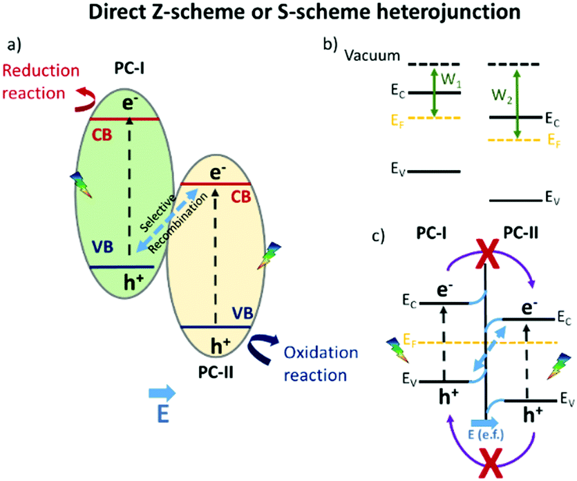
The formation of heterojunctions at semiconductor interfaces results in band alignment, which can occur in different manners depending on the band potentials. The best performance for this technology has turned out to be for interfaced systems in which the band gaps of the semiconductors are staggered with the subsequent improvement of the charge carrier separation,22 as depicted in Scheme 1; this development has gone down in history as the type-II heterojunction.
 | ||
| Scheme 1 Type-II heterojunction. Charge carrier separation model at the semiconductor interface characterized by staggered band gaps. | ||
The enhanced photocatalytic achievements reside in the fact that the photo-generated charge carriers are stabilized on two different semiconductors, achieving limited electron–hole pair recombination. An inherent restriction of this model is that the holes and electrons are not stabilized on semiconductors with the best oxidative and reductive potentials, respectively. This problem has recently been overcome by the so called “direct Z-scheme” or “S-scheme” heterojunction, already conceptually theorized by Bard in 1979:23 the first direct Z-scheme-interfaced systems could only be constructed in the liquid phase, since they needed the presence of an electrolytic mediator.24 In 2006, Tada et al.25 demonstrated that an all-solid Z-scheme was possible, in which the solid electron mediator was represented by gold particles. However, it was just in 2013 that direct Z-scheme heterojunction engineering was proposed, flanking two semiconductors without electron mediators,26 whose charge carrier dynamics is sketched in Scheme 2.
 | ||
| Scheme 2 Interface charge carrier migration in a “direct Z-scheme” or “S-scheme” heterojunction. | ||
The novel technology is achieved, similarly to a type-II heterojunction, when two semiconductors characterized by staggered band gaps are put in contact; but this time, a suitable work function, an intrinsic feature of the two materials, allows the formation of a peculiar electric field at the interface. Due to the existence of an internal electric field coming from the different work functions of the two semiconductors (b) and (c) in Scheme 2, the selective recombination of photoinduced electrons in the semiconductor with the lower CB (PCII) and the holes in the semiconductor with the higher VB (PCI) occurs. This still guarantees the spatial separation of the photoinduced charge carriers that, different from the classical type-II heterojunction, are available at the best redox potentials.27–29
In the last decade, the long-time known material g-C3N4 has come back into the limelight in the field of heterogeneous photocatalysis. Indeed, although it was first synthetized in 1834 by Berzelius and Liebig,30 it was only proposed as a suitable polymeric semiconductor for photocatalytic applications, based on earth-abundant elements, in 2009 by Wang et al.31 In their study, the researchers proved the unique photocatalytic ability of g-C3N4, derived by the direct heating of a cyanamide precursor in air at different temperatures, in the production of H2 from the water photo-splitting process upon visible light irradiation. As a matter of fact, the growing interest in the promising photocatalytic performance shown by the metal-free visible active polymeric g-C3N4 resulted in almost a quarter of the overall photocatalysis research literature focusing on this subject in 2019. However, despite the undoubted promising properties characterizing a promising photocatalyst exhibited by g-C3N4, such as a band gap capable of absorbing visible photons of 2.7 eV,31,32 modification ability of the band gap through thermal treatments33–35 and a CB potential able to reduce H2O and CO2 molecules, some drawbacks have limited its practical application. Indeed, the high electron–hole recombination rate, the low quantum and separation efficiencies and the small specific surface area resulted in large nanoparticles dramatically affecting the photocatalytic performance. Hence, the need to tune in a proper way the material features by means of doping,36,37 morphological modifications to increase the surface area, tuning the synthesis parameters and employing soft and hard templates38–41 for the development of intrinsic defects42,43 and the formation of heterojunctions with other semiconductors such as TiO2, ZnO and WO3 has become paramount.44–48 This last strategy has produced the best results, delaying electron–hole recombination since the photoinduced charge carriers are stabilized on the two different materials.
By the way, several inferences have corroborated the best performance of the g-C3N4-based heterojunction systems, most of the time as result of the enhanced photocatalytic reaction. However, the working mechanism, governing the charge carriers separation enhance, remained often unexplained.
In this work, the C3N4–ZnO visible photoactive system, with proven ability in photocatalytic oxidation and reduction,46,47,49–54 has been synthetized and investigated mainly from the optical and electronic points of view. The most used technique for this purpose is electron paramagnetic resonance (EPR) spectroscopy, able to give a deep view of the electronic states of solids, and used to follow charge carrier separation upon in situ irradiation and to depict a direct and clear overview of the electron and hole dynamics at the semiconductor interfaces. To the best of our knowledge, this study provides straightforward and unambiguous proof of the direct Z-scheme or S scheme heterojunction mechanism of the visible photon absorption characterizing the C3N4–ZnO mixed system.
2. Materials and methods
2.1 Sample preparation
Melamine (C3H6N6) and zinc nitrate hexahydrate (Zn(NO3)2·6H2O) employed in the preparation of the samples were purchased from Sigma-Aldrich and used without any further purification treatment.The 50![[thin space (1/6-em)]](https://www.rsc.org/images/entities/char_2009.gif) :50 C3N4–ZnO mixture was synthetized from an aqueous 1 M (V = 20 ml) solution of the respective precursors (C3H6N6 and Zn(NO3)2·6H2O) kept under constant stirring for one hour at room temperature. The sample was further collected and dried at 353 K. The final material was obtained by thermal annealing in air at 823 K for 4 h with a temperature ramp of 5 °C min−1.
:50 C3N4–ZnO mixture was synthetized from an aqueous 1 M (V = 20 ml) solution of the respective precursors (C3H6N6 and Zn(NO3)2·6H2O) kept under constant stirring for one hour at room temperature. The sample was further collected and dried at 353 K. The final material was obtained by thermal annealing in air at 823 K for 4 h with a temperature ramp of 5 °C min−1.
The pristine samples of g-C3N4 and ZnO were produced following the same procedure adopted for the mixed system.
2.2 Characterization methods
X-ray powder diffraction (XRPD) patterns, acquired to define the structural phases and the crystallinity of the samples, were recorded using a PANalytical PW3040/60 X’Pert PRO MPD diffractometer using a copper Kα radiation source (0.154056 nm). The intensities were obtained in the 2θ range between 10° and 80°. X’Pert High-Source software was used for data handling.UV-Visible absorption spectra were recorded using a Varian Cary 5 spectrometer, coupled with an integration sphere for diffuse reflectance (DR) acquisition, using Carywin UV/scan software. A sample of PTFE with 100% reflectance was employed as reference. Spectra were recorded in the 200–800 nm range at a scan rate of 240 nm min−1 with a step size of 1 nm. The measured intensities were converted using the Kubelka–Munk function. The energy gap has been evaluated using the Tauc plot method.55
Transmission electron microscopy analysis was performed at our institute, using a high resolution transmission microscope, TEM JEOL JEM-3010, operated at 300 keV. The microscope was equipped with a Gatan US1000 CCD camera and Energy Dispersive Detector OXFORD Software INCA.
The electronic paramagnetic resonance measurements were conducted using a CW-EPR EMX-Bruker spectrometer operating at the X-band (9.5 GHz), equipped with a cylindrical cavity operating at 100 kHz field modulation and interfaced with a computer with the WINEPR Acquisition program. The spectra were recorded in a bath of liquid nitrogen (77 K). Prior to the measurements, the samples underwent an activation treatment, aimed at cleaning the surface from absorbed and physisorbed species (hydroxyl and carboxyl groups), obtaining a more stoichiometric compound at the surface, and allowing a more efficient study of the charge carrier separation. The treatment provides a first annealing step in which the materials were heated in a dynamic vacuum at 573 K for 30 minutes; following this, 50 mbar of molecular oxygen was added and the temperature was raised up to 673 K. At the end of the treatment, the excess molecular oxygen was removed and the measurements were performed under a vacuum condition. The photoactivity of the synthetized material was investigated by using coupled EPR spectroscopy with in situ irradiation, using a 1000 W xenon lamp (Oriel Instruments) equipped with an IR water filter, to which different band pass filters (Newport-20CGA, UV filter cutting visible light components, λ ≥ 400 nm, λ ≥ 420 nm and λ ≥ 455 nm) were applied. Computer simulation of the EPR spectra was performed using the SIM32 software developed by Prof. Sojka (Jagellonian University, Cracow, Poland).56
3. Results
3.1 Structural and morphological analysis
XRPD analysis was executed on the synthetized samples and is reported in Fig. 1, which displays the bare ZnO reflections corresponding to the (100), (002), (101), (102), (110), (103), (200), (112), (201), (004) and (104) planes, typical of the wurtzitic hexagonal crystal phase (JCPDS 36-1451);57 the reflection sharpness and the absence of further signals confirm the highly pure and crystalline nature of the sample. The diffractogram related to the pure g-C3N4 material is characterized by two reflections at 2θ = 27.3° and 2θ = 13.2°, respectively (JCPDS 87-1526): the first one, with the strongest intensity, is associated with the (002) crystal planes of the conjugated stacking aromatic system typical of graphitic materials38,58 with a distance of 0.326 nm, while the second reflection, weaker and broader, is attributed to the (100) crystal planes of the in-plane structural packing motif of the tri-s-triazine (melem) units.59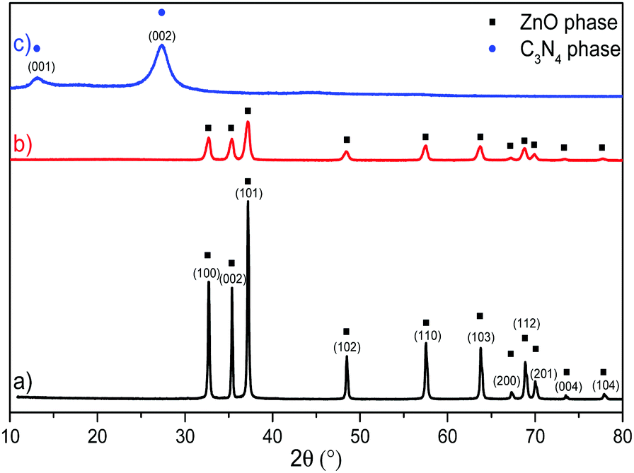 | ||
| Fig. 1 XRPD analysis of: (a) bare ZnO (black line), (b) g-C3N4–ZnO (50:50 mixture) (red line) and (c) bare g-C3N4 (blue line). | ||
The diffractogram of the 50:50 C3N4–ZnO mixture reveals a significant change considering the XRPD patterns of both pristine samples, where the g-C3N4 structural fingerprints are not present and the reflections of the ZnO phase are considerably reduced, forming a broader profile; however, a 2θ shift was recorded, indicating the existence of unmodified wurtzitic ZnO phase in the mixed sample without the incorporation of external species. Accordingly, the lower intensity and the larger width of the reflections represent a smaller crystal size and a loss in crystallinity in the case of the two-phase systems compared to those of the bare ones. The reduced crystallinity of the mixed material is ascribable to the concurrent crystallization of ZnO that hinders the condensation process and the interlayer stacking of the g-C3N4 phase; in contrast, the growth of the ZnO nanocrystals is also delayed by the presence of g-C3N4.50,53
The TEM pictures acquired for the mixed material, shown in Fig. 2, allow the verification of the existence of the C3N4 phase, undetectable by XRPD, and its intimate contact with the ZnO phase.
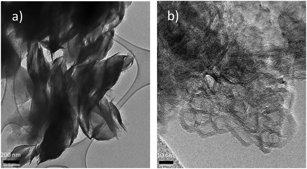 | ||
| Fig. 2 TEM images of C3N4–ZnO (50:50). | ||
As shown in Fig. 2(a), the C3N4 phase in the mixed system appears as petal brushstrokes painted on the surface of ZnO nanoparticle structures. At higher magnitudes (Fig. 2(b)), ZnO nanocrystals surrounded by the typical multilayer staking structure of the graphitic carbon nitride can be recognised, confirming that the synthetic procedure has enabled the formation of an interfaced system: as will be presented in the following sections, the occurrence of such a connection between the two semiconductors leads to a unique form of charge carrier transport.
3.2 Optical characterization
UV-vis DR spectroscopy has been employed to evaluate the optical behaviour and the electronic structure of the synthetized materials. The semiconducting nature of ZnO, characterized by a direct band gap, appears in spectrum (a) of Fig. 3 with the typical absorption in the UV range up to 375 nm. As widely reported in previous works, it is caused by the electron transition from the valence band, mainly formed by 2p orbitals of O2−, to the conduction band, made up by the 4s states of Zn2+. The band gap value, calculated with the Tauc plot method,55 is in line with those found in the literature and evaluated to be 3.3 eV.60–65 As reported in previous studies, the direct poly-condensation of the melamine precursor performed at 823 K in air produces C3N4 in the graphitic phase, with a band gap of 2.7 eV, making it a material able to absorb photons in the visible range, up to almost 460 nm.31,32,34,66–68 The UV-vis spectrum (c) in Fig. 3 shows this feature, in which the electrons in the VB, predominantly constituted by the pz orbitals of nitrogen, are photoexcited by visible photons, up to energies corresponding to wavelengths around 460 nm, into the conduction band, composed of the pz orbitals of carbon atoms.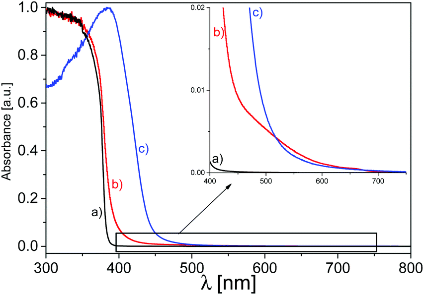 | ||
| Fig. 3 Normalized UV-vis DR spectroscopy measurements of: (a) pristine ZnO (black line), (b) C3N4–ZnO (50:50) (red line) and (c) g-C3N4 (blue line). | ||
Concerning the optical analysis of the 50:50 mixed system (spectrum b), (Fig. 3), it exhibits a red-shift of the absorption edge with a band gap value of 3.1 eV with respect to that of pristine ZnO, where the visible photon absorption improvement is attributed to the presence of the C3N4 phase, suggesting a close cooperation of the two phases at the interface. The zoomed-in view shown in Fig. 3 ascertains that the mixed material shows a slightly higher absorption of photons at longer wavelengths compared with bare g-C3N4, probably due to the higher defectiveness of this phase in the mixed system as a result of the simultaneous crystallization with the ZnO phase during C3N4 condensation, as already discussed in previous works.37,49,50,52 It should be noted that the absorption of the C3N4–ZnO interface is higher also in the UV range with respect to g-C3N4, thanks to the presence of ZnO. Then, it can be attested that the contemporary presence of the two phases is beneficial in terms of there being a wider range of photons absorbed with respect to the bare materials, both in the UV and visible ranges, revealing an intimate cooperation of the two phases during the light absorption determined by a successful charge carrier transfer at the interfaces.
3.3 EPR spectroscopic study upon exposure to irradiation
In general, electron paramagnetic resonance (EPR) spectroscopy is a highly sensitive magnetic resonance technique based on the energy separation of the spin states of an unpaired electron by the action of an external magnetic field, exploiting the electronic Zeeman effect, in which the magnetic transitions are induced by microwave photons (in the range of GHz). In the last decades, its potentiality in the huge panorama of heterogeneous catalysis has increased, with particular emphasis in the field of photocatalysis.69,70 This has been possible since EPR has proven to be a sensitive tool for the monitoring of charge carrier separation, with the carriers very often trapped in intrinsic or extrinsic defect sites during light absorption, generating paramagnetic species. In this sense, EPR can be considered as an analytical technique that can be used to perform a pre-screening of material photoactivity.71,72 In addition, it is increasingly used to obtain supporting analysis to determine the working mechanism upon light absorption of complex materials or heterojunctions,73–75 in such a way as to achieve the correct electronic transfer at the interface, as will be presented in the following.Connecting the discussion to transition metal oxide semiconductors, it is well known that, considering the band structure whereby they are modelled, when a semiconducting material is irradiated by a suitable light energy, the excitation of electrons (negatively charged) from the valence band to the conduction band occurs, leaving the holes (positively charged) in the valence band and generating charge carrier separation; this phenomenological occurrence is reported in eqn (1):
| MeOX + hν → e(CB)− + h(VB)+ | (1) |
In this regard, when the irradiation is conducted under vacuum conditions (where no surface molecules can interact with the excited charge carriers) and at a low enough temperature, such as that of liquid nitrogen (77 K, to prevent electron–hole pair recombination), it is possible to follow the photo-generation of electrons and holes that, stabilized in the solid, induce paramagnetic species peculiar to each solid.
As is obvious, the stabilization of photo-generated charge carriers depends on the nature of the oxide matrix, but some guidelines can be summarized. The photoexcited electrons are generally stabilized on metal cations, as described by eqn (2), forming shallow donor energetic levels just below the conduction band edge.
| Men+ + e− → Men−1 | (2) |
In this way, the ionized metal cation becomes a paramagnetic centre, easily recognizable via EPR.
On the other hand, the photoinduced holes are stabilized at the oxygen ions of the lattice (O2−), ionizing them to the paramagnetic species O−, as outlined hereafter in eqn (3):
| O2− + h(VB)+ → O− | (3) |
Transferring the acquired knowledge to the materials of this study, in Fig. 4, the EPR spectrum of pristine ZnO after the activation process (see Materials and methods section) is shown before and during the exposure to UV light irradiation. As confirmed by the UV-vis spectra(Fig. 3), the synthetized ZnO is photoactive just in the UV range of the electromagnetic spectrum, with no activity under visible light. The spectrum (a) of Fig. 4 shows that ZnO displays some EPR signals before the illumination procedure, due to the lack of a perfect stoichiometry in the sample, where, in order to maintain charge neutrality, several defects are generated, among which some have paramagnetic character. Upon UV exposure, the profile of the spectrum does not change qualitatively, but one witnesses an intensity increase of the EPR signals. In detail, the quasi-isotropic line with g < ge (right hand side of the spectra, ge = 2.0023 is the free electron g value) at g = 1.96 is caused by electrons excited in the conduction band and relaxed in shallow donor levels, at around 0.02–0.05 eV below the conduction band edge. The shallow donor nature has been, in the past, the subject of several different attributions among which are oxygen vacancies (or F-centres),76–78 interstitial zinc,79–84 group-III element impurities85–87 and interstitial hydrogen.88–90 Although the assignment to oxygen vacancies is nowadays considered erroneous, since the theoretical calculations confirmed their location in the middle of the ZnO band gap instead of being shallow,65,91 the signal's origin still lacks a clear and defined explanation. An unambiguous answer is complicated by the fact that the isotopic abundance of 67Zn (I = 5/2, giving a six line multiplicity for the hyperfine interaction) is lower than 5%, preventing the observation of any resolved hyperfine interaction that could provide direct information about the chemical nature of the donors. In addition, an isotropic line has been observed in highly pure ZnO single crystals, making the hypothesis that it could be caused by III-group elements less convincing. However, all researchers agree with the fact that the signal at g = 1.96 is derived from the electrons in the conduction band or trapped in the shallow donor levels; in the latter case, the signal seems to be independent of the shallow donor identity92,93 and the electrons can be modelled in an effective-mass-hydrogenetic-like state.94
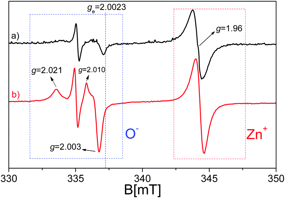 | ||
| Fig. 4 EPR spectra of pristine ZnO recorded at 77K and in a vacuum after the activation treatment: (a) in the dark (black line) and (b) upon UV irradiation (red line). | ||
In line with the above mentioned debate, the signal enhancement upon UV irradiation is attributed to the photoexcitation of electrons from the valence band to the conduction band or in shallow donor levels. The mechanism reported in eqn (4) is therefore purely formal but consistent with the EPR study of other transition metal oxide semiconductors, where the photoexcited electrons are stabilized on specific cations (e.g. Ti3+ in TiO2 and Zr3+ in ZrO269,72).
| Zn2+ + e− → Zn+ | (4) |
The growth of a complex signal at g > ge (left-hand side of the spectra) constituted by two axial signals with g‖ = 2.019 and g⊥ = 2.005 and g‖ = 2.010 and g⊥ = 2.004 upon irradiation is caused by the trapping of photo-generated holes, taking place according to eqn (3).78,81,95–98
After having ascertained that the stabilization of charge carriers upon UV irradiation can be followed via EPR spectroscopy for ZnO, we shift the matter of the discussion to the bare g-C3N4 semiconductor. Before analysis of the EPR outcomes for the graphitic polymer, it is worth considering its electronic configurations and their hybridization. Considering the carbon in the N![[double bond, length as m-dash]](https://www.rsc.org/images/entities/char_e001.gif) C–N2 bond of the tri-s-triazine ring in the ground state, the 2s orbital is filled with two electrons with opposite spins, as well as the 2px and 2py sublevels of the 2p orbitals, while the 2pz orbital is unoccupied. Passing to the excited state, with each of the 2px, 2py and 2pz orbitals occupied by an unpaired electron, the 2s orbital can hybridize with 2px and 2py, giving rise to three sp2 hybridized orbitals (equivalently hybridized), leaving the unpaired electrons in the 2pz state, at slightly higher energy. The same argument can be applied for the N atom in both the C–NC and in the N–(C)3 bonds: while in the first case, the excited state is characterized by an sp2 hybridization, this time non-equivalent (one of the three sp2 hybridized orbitals is doubly occupied) but again with un unpaired electron in the 2pz orbital, in the second case, an equivalent sp2 hybridization can be considered anew with the 2pz orbital doubly occupied. Having elucidated the atomic configuration in the tri-s-triazine unit constituting the heptazine network of g-C3N4, the overlapping of the sp2 hybridized orbitals of C and N atoms results in the formation of σ-bonds, while the overlapping of the 2pz orbitals generates π-bonds. In the latter case, the electrons, half coming from the carbon atoms and half coming from N atom subunits, cannot be confined but they are free, constituting the π-conjugated structure.99 It should be noted that the two electrons with different spin orientation in the 2pz orbitals of the N atom in the N–(C)3 bonds do not take part in the delocalized π-conjugated system due to the Coulombian repulsion to which they are subjected; in this case, the electrons in the π-conjugated system cannot move in the 2D plane but they can travel inside the triazine ring, leading to a localized π-conjugated structure, as described by DFT calculations in ref. 32.
C–N2 bond of the tri-s-triazine ring in the ground state, the 2s orbital is filled with two electrons with opposite spins, as well as the 2px and 2py sublevels of the 2p orbitals, while the 2pz orbital is unoccupied. Passing to the excited state, with each of the 2px, 2py and 2pz orbitals occupied by an unpaired electron, the 2s orbital can hybridize with 2px and 2py, giving rise to three sp2 hybridized orbitals (equivalently hybridized), leaving the unpaired electrons in the 2pz state, at slightly higher energy. The same argument can be applied for the N atom in both the C–NC and in the N–(C)3 bonds: while in the first case, the excited state is characterized by an sp2 hybridization, this time non-equivalent (one of the three sp2 hybridized orbitals is doubly occupied) but again with un unpaired electron in the 2pz orbital, in the second case, an equivalent sp2 hybridization can be considered anew with the 2pz orbital doubly occupied. Having elucidated the atomic configuration in the tri-s-triazine unit constituting the heptazine network of g-C3N4, the overlapping of the sp2 hybridized orbitals of C and N atoms results in the formation of σ-bonds, while the overlapping of the 2pz orbitals generates π-bonds. In the latter case, the electrons, half coming from the carbon atoms and half coming from N atom subunits, cannot be confined but they are free, constituting the π-conjugated structure.99 It should be noted that the two electrons with different spin orientation in the 2pz orbitals of the N atom in the N–(C)3 bonds do not take part in the delocalized π-conjugated system due to the Coulombian repulsion to which they are subjected; in this case, the electrons in the π-conjugated system cannot move in the 2D plane but they can travel inside the triazine ring, leading to a localized π-conjugated structure, as described by DFT calculations in ref. 32.
In light of the clarified atomic configuration characterizing the atoms of the heptazine network constituting the building blocks of the investigated C3N4, its EPR spectrum in Fig. 5 can be readily analysed. As reported in many previous works,33,34,100,101 the spectrum of thermally activated g-C3N4, before light exposure, shows an isotropic line with a mostly Lorentzian shape at g = 2.0042, caused by unpaired electrons in the localized π-conjugated system, with preferential carbon character; this assignation is supported by the absence of hyperfine splitting typical of unpaired electrons stabilized on N atoms. The presence of unpaired electrons in the localized excited state prior to illumination can be attributed to defects in the nanostructured material caused by melamine polymerization.99,102,103
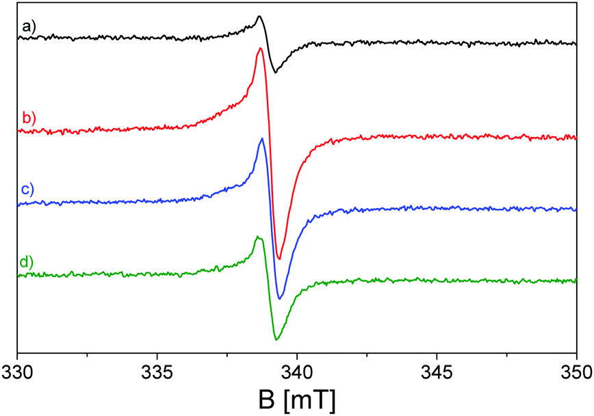 | ||
| Fig. 5 EPR spectra of pristine g-C3N4 recorded at 77 K and in a vacuum after the activation treatment: (a) in the dark (black line), and (b) upon illumination with a band pass filter at λ ≥ 400 nm (red line); (c) at 420 nm (blue line) and (d) at 455 nm (green line). | ||
Upon visible light irradiation, performed with several band pass filters at different visible wavelengths of irradiation, the rising up of the Lorentzian line, due to the electron photoexcitation from the valence band (2p nitrogen orbitals) to the conduction band (2p carbon orbitals), dominates the EPR spectra (b–d) of Fig. 5, increasing the number of unpaired electrons in the localized π-conjugated system. It can be observed that the outcomes are in line with the UV-vis spectroscopy measurements (Fig. 3), since the g-C3N4 material is still photoactive under irradiation executed with λ ≥ 455 nm, although the intensity of the signal decreases, as can be seen, with increasing irradiation wavelength.
Upon further analysis of the EPR spectra during the irradiation procedure, a further broader shoulder is visible at lower magnetic field values and is attributed to electrons trapped at nitrogen radicals in the polymeric network.100 In order to evaluate this hypothesis, simulation of the EPR spectra of the g-C3N4 sample upon irradiation with λ ≥ 400 nm has been carried out using the SIM32 software:56Fig. 6 reports the calculated spectrum in comparison with the experimental one, where the single convolutions are also highlighted.
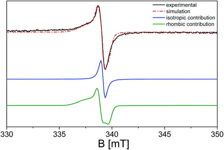 | ||
| Fig. 6 Simulation of the EPR spectra of pristine g-C3N4 recorded at 77 K and in a vacuum after the activation treatment upon illumination at λ ≥ 400 nm: experimental (black line), simulated (red dashed line), Lorentzian convolution (blue line), and rhombic convolution (green line). | ||
The simulation confirms the presence of a further species with respect to the most imposing Lorentzian character at g = 2.0042 (blue line in Fig. 6), distinguished by a rhombic shaped signal with g1 = 2.0150, g2 = 2.0062 and g3 = 2.0012 (green line in Fig. 6), compatible with the presence of nitroxide species generated during the surface oxidation of the activation treatment.104–107 The broad profile displayed by the g1 component of the rhombic signals is imputable to the inhomogeneity of the nanocrystal surface, in which the unpaired electrons can differently interact with the neighbouring species.
Regarding the EPR characterization of the C3N4–ZnO mixed system, as shown in Fig. 7, a much more complex profile appears. To the best of our knowledge, this study provides the first investigation of paramagnetic centres regarding the interfaced system C3N4–ZnO. In order to streamline the analysis, the first step is to refer back to the EPR features observed for the two bare semiconductors, again by means of a simulation procedure (red line spectrum in Fig. 7).
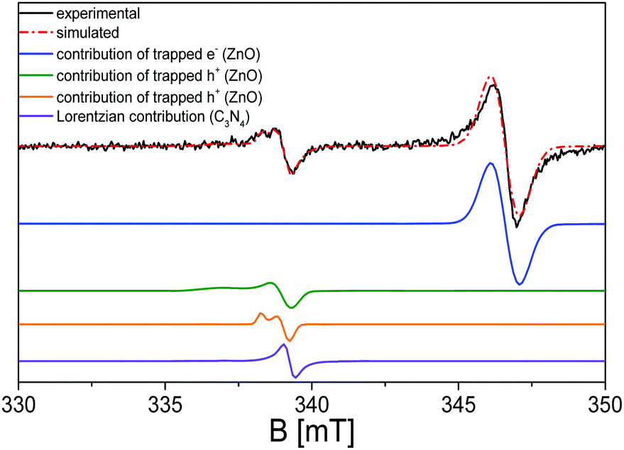 | ||
| Fig. 7 EPR spectrum of the 50:50 C3N4–ZnO mixed system and the corresponding simulation: experimental (black line), simulation (red dashed line), contribution from the isotropic line at g = 1.96 (trapped electrons) of ZnO (blue line), contribution from the axial line at g‖ = 2.019 and g⊥ = 2.005 (trapped holes) of ZnO (green line), contribution from the axial line at g‖ = 2.010 and g⊥ = 2.004 (trapped holes) of ZnO (orange line), and contribution from the isotropic line at g = 2.0042 (trapped electrons) of C3N4 (violet line). | ||
The various deconvolutions in the calculated spectrum reveal the EPR signals already observed and described for the two separate ZnO and C3N4 phases: the spectrum is dominated by the isotropic line at g = 1.96 due to electrons trapped in the shallow donor levels of ZnO. The signal at lower magnetic fields appears more complicate with respect to that generated by the trapped holes (O−) in the pristine ZnO, due to the presence of the Lorentzian signal at g = 2.0042 caused by the electrons stabilized at the localized π-bonds, and characterized by the carbon character.
The exposure of the mixed material C3N4–ZnO to visible irradiation produces a modification of the EPR spectrum in terms of signal intensities completely different with respect to what is observed for the pristine samples. Fig. 8 shows the mixed material upon exposure to light with λ ≥ 400 nm (red line) and λ ≥ 455 nm (blue line).
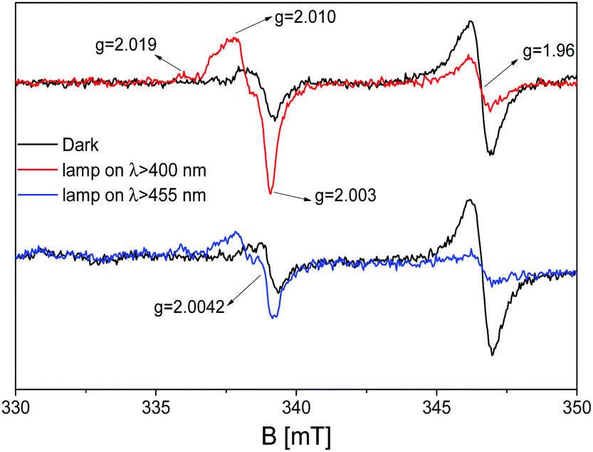 | ||
| Fig. 8 EPR spectra of pristine g-C3N4 recorded at 77 K and in vacuum after the activation treatment: dark (black line), upon illumination with a band pass filter at λ ≥ 400 nm (red line) and at λ ≥ 455 nm (blue line). | ||
Opposite to bare ZnO, in which UV irradiation causes a growth of the signal at g = 1.96 due to the stabilization of photoexcited electrons in shallow donor levels (Fig. 4), for the mixed sample, the intensity of the signal drops down during the visible light exposure performed with band pass filters at 400 nm and 455 nm. On the other hand, the more complex signals at higher g values, having axial character and attesting to the stabilization of the photoinduced holes stabilized as O− species in ZnO, grow during irradiation as in the case of the pristine material in the case of UV illumination. Finally, the isotropic Lorentzian line at g = 2.0042, caused by the localized electrons in C3N4, is embedded in the broader g⊥ component of the O− centres, as certified by the simulation in Fig. 7 (violet line). This implies that the 50:50 C3N4–ZnO mixture is photoactive upon visible irradiation, improving the photoactivity feature of the zinc oxide; the observed trend guarantees a beneficial interfacing between the two semiconducting materials in which the charge carrier separation can be analysed and elucidated as discussed in the following section.
3.4 Results and discussion and unveiling of visible photon absorption mechanism
Summarizing the presented results, the synthetized ZnO, characterized by a wurtzitic crystal structure, undergoes charge carrier separation upon UV irradiation that can be followed using EPR spectroscopy by means of well-established strategies, in which the signals of trapped photoinduced charge carriers can be recognized in the spectrum, located in separate spectral regions.69,70,98 Concerning the pristine g-C3N4, obtained by the poly-condensation of the melamine precursor via annealing in air at 823 K, it showed a typical 2D graphitic structure composed of tri-s-triazine units dominated by a π-conjugated system. Also, in this case, the excitation of electrons upon visible irradiation has been recognised by means of EPR spectroscopy, with the increase of the Lorentzian line at g = 2.0042 due to the stabilization of excited electrons in the localized π-bonds, having carbon character and forming the material conduction band; moreover, the presence of the surface nitroxide radicals has been verified, having a specific rhombic g-tensor. The activity at different photon frequencies of the two pristine materials was confirmed by means of UV-vis spectroscopy measurements, highlighting the photo absorption of ZnO just in the UV spectral region, while for g-C3N4, the absorption edge is around 460 nm. The 50:50 mixture has exhibited a red-shift with respect to bare ZnO of the absorption edge and a slightly higher absorption in the visible region compared to that of pure g-C3N4, indicating an actual cooperation of the two phases in the interfaced system. TEM imaging confirmed the homogenous distribution of the two phases and their anchoring one around the other, suggesting an active partnership at the interface and constituting a heterojunction system.
In the last years, several authors have reported the prominent photocatalytic ability upon visible light exposure of the mixed C3N4–ZnO material,47,49,54,108,109 where they speculated the working mechanism at the interface of the heterojunction. In most of the cases, the sustained hypothesis of the real process upon visible photonic irradiation foresees an electron transfer from the C3N4 conduction band (−1.12 eV vs. NHE) to the ZnO conduction band (−0.02 eV vs. NHE), typical of a type-II heterojunction or a p–n heterojunction. In contrast, the hole transition would occur from the ZnO valence band (+3.00 eV vs. NHE) to the C3N4 valence band (+1.57 eV vs. NHE) (Scheme 3). In general, in a type-II heterojunction, the spatial charge carrier separation is improved, since the photo-generated charge carriers are localized on the two different semiconductors; however, the stabilized electrons and holes are not at the best potentials for reductive and oxidative redox reactions, respectively. These explanations are not consistent with the extremely high photocatalytic activity exhibited by the C3N4–ZnO mixed system in both oxidative and reductive reactions.
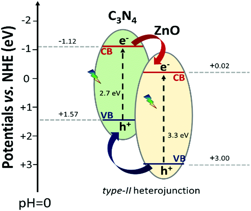 | ||
| Scheme 3 Schematic representation of the hypothetical C3N4–ZnO type-II heterojunction with the standard potential found in the literature.50 | ||
Accordingly, considering the outcomes of this work obtained by using the EPR technique upon in situ visible irradiation of C3N4–ZnO and compared with the results of the pure materials, it is clear that a different mechanism of charge carrier migration at the interface should be considered. Indeed, in the case that the working mechanism is the one described above (type-II heterojunction, Scheme 3), the signal at g = 1.96 in the mixed system should grow, in a similar way as in ZnO during UV light exposure, but this is not the case. In contrast, in C3N4–ZnO, the signal at g = 1.96 decreases, both with irradiation performed with band pass filters at λ ≥ 400 nm and λ ≥ 455 nm, indicating that an electron transition occurs from ZnO during the illumination; still, the hole signal (O−), at higher g values, rises in a conspicuous way compared to the holes in bare ZnO, although the irradiation was more energetic (UV) for the pristine material.
This elucidation of the results allows us to sustain the hypothesis proposed by a few researchers, in which they suggested a different electron transition with respect to that of the type-II heterojunction, but without enough convincing mechanistic studies and just derived from photocatalytic reactions.50 Rather, the charge transfer at the interface of C3N4–ZnO during visible light irradiation can be explained with the recently proposed “direct Z-scheme or S-scheme” heterojunction.24,29,110,111 In this case, the band alignment configuration at the interface is the same as that of the type-II heterojunction, where the band gaps of the two semiconductors are staggered. The different charge carrier dynamics at the interface is guaranteed by a suitable work function difference at the interface between the two semiconductors, a fundamental prerequisite inducing a specific electric field at the interface. The establishment of the electric field at the interface (derived from the peculiar features of the semiconductors) favours the selective annihilation of the electrons from the semiconductor with the lower conduction band (ZnO in this case) energy and that of the holes from the semiconductor with the higher valence band energy (C3N4). The described charge carrier transportation would ensure the strongest redox ability for the photoexcited electrons stabilized in the C3N4 conduction band and that of the photoinduced holes in the ZnO valence band, as depicted in Scheme 4.
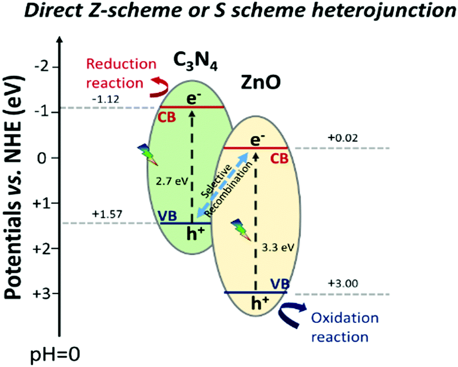 | ||
| Scheme 4 Schematic representation of the actual C3N4–ZnO “direct Z-scheme” or “S scheme” heterojunction with the standard potential found in the literature.50 | ||
In conclusion, EPR spectra upon visible irradiation recording both the simultaneous reduction of the electronic signal (g = 1.96) and the improvement of the hole signals of ZnO must be explained by the recombination at the interface of the photoexcited electrons in ZnO with the holes of C3N4 (not detected by EPR).
The consistency of these results provides solid proof of the supposed working mechanism occurring during visible irradiation of the C3N4–ZnO mixed system, unraveling the predictions of previous studies. Nevertheless, the necessity of a scale-up concerning the production of H2 from the water photo-splitting reaction or CO2 photo-reduction reaction in chemical products requires further improvements starting from the synthetic routes, aiming obtain more highly porous materials, then with a higher specific surface area available for the reactions at the surface, and to ensure a greater intimate contact at the interface to further enhance the charge carrier annihilation at the semiconductor surfaces.
4. Conclusions
Bare ZnO and C3N4 semiconducting materials and the 50:50 C3N4–ZnO mixture were prepared via a fast and facile synthetic route, consisting of a one-step annealing in air of the dissolved precursors at a moderate temperature (823 K) for 5 hours. Structural and morphological analyses have revealed the purity of the obtained phases, expressed in a diffraction pattern of the typical wurtzitic hexagonal phase for ZnO and of the characteristic repetition of the interlayer stacking of the aromatic systems for the C3N4 graphitic phase; moreover, the existence of an intimate contact between the two phases for the mixed material emerged, unveiling the formation of an interfaced system. Optical measurements performed with UV-vis DR spectroscopy testified a band gap of 3.3 eV for the bare ZnO and of 2.7 eV for the pristine g-C3N4, while the C3N4–ZnO sample showed greater light absorption in all the spectral ranges.
The working mechanism upon visible light absorption of the C3N4–ZnO heterojunction has been investigated by coupling EPR spectroscopy with in situ irradiation performed employing different band pass filters and comparing the outcomes with those of the pristine materials. It was found that bare ZnO displayed an increase of the signals due to the trapping of photoexcited electrons (g = 1.96) and holes (g‖ = 2.019 and g⊥ = 2.005 and g‖ = 2.010 and g⊥ = 2.004), inducing paramagnetic defects; on the other hand, g-C3N4 also exhibited an increase of the Lorentzian line at g = 2.0042 upon visible irradiation, caused by the photoexcitation of the electrons from the valence band (with almost nitrogen character) to the conduction band (derived from the pz carbon orbitals of the π-conjugated system). Concerning the mixed system, opposite behaviour was recorded during visible illumination, where the signal due to the trapped electrons in the ZnO matrices decreased, while the hole signals still increased. The observed phenomenon can only be only explained by assuming a direct Z-scheme or S-scheme heterojunction at the material interfaces, as previously reported in a few works, and not to a type-II heterojunction as often theorized. To the best of our knowledge, this study provides the first experimental evidence regarding a definitive attribution of the visible light absorption mechanism of the C3N4–ZnO heterojunction.
Conflicts of interest
The authors declare no competing financial interest.Acknowledgements
Financial support from the Italian MIUR through the PRIN Project 20179337R7, MULTI-e “Multielectron transfer for the conversion of small molecules: an enabling technology for the chemical use of renewable energy” is gratefully acknowledged.Notes and references
- E. C. C. Baly, I. M. Helilbron and W. F. Barker, J. Chem. Soc., 1921, 119, 1025–1035 RSC.
- J. M. Coronado, F. Fresno, M. D. Hernández-Alonso and R. Portela, Design of Advanced Photocatalytic Materials for Energy and Environmental Applications, London, 2013 Search PubMed.
- D. F. Ollis, E. Pelizzetti and N. Serpone, Environ. Sci. Technol., 1991, 25, 1522–1529 CrossRef CAS.
- M. R. Hoffman, S. T. Martin, W. Choi and D. W. Bahnemann, Chem. Rev., 1995, 95, 69–96 CrossRef.
- K. Maeda and K. Domen, J. Phys. Chem. Lett., 2010, 1, 2655–2661 CrossRef CAS.
- K. Domen, J. N. Kondo, M. Hara and T. Takata, Bull. Chem. Soc. Jpn., 2000, 73, 1307–1331 CrossRef CAS.
- T. Inoue, A. Fujishima, S. Konishi and K. Honda, Nature, 1979, 277, 637–638 CrossRef CAS.
- X. Chang, T. Wang and J. Gong, Energy Environ. Sci., 2016, 9, 2177–2196 RSC.
- S. Jerez, J. M. Lopez-Romero, M. Turco, P. Jimenez-Guerrero, R. Vautard and J. P. Montavez, Nat. Commun., 2018, 9, 1304 CrossRef CAS.
- C. Figures, H. J. Schellnhuber, G. Whiteman, J. Rockström, A. Hobley and S. Rahmstorf, Nature, 2017, 546, 593–595 CrossRef.
- A. Hernandez-Ramirez and I. Medina-Ramirez, Photocatalytic Semiconductors, 2015 Search PubMed.
- L. L. Basov, Y. U. P. Solonitsyn and A. N. Terenin, Dokl. Akad. Nauk SSSR, 1965, 122–124 CAS.
- L. L. Basov, G. N. Kuzmin, L. M. Prudnikov and Y. U. P. Solonitsyn, LGU Leningrad, 1976, 82–120 Search PubMed.
- K. Ranabhat, L. Patrikeev, A. Antal'evna-Revina, K. Andrianov, V. Lapshinsky and E. Sofronova, ARPN J. Eng. Appl. Sci., 2016, 14, 481–491 CrossRef.
- A. V. Emeline, V. N. Kuznetsov, V. K. Ryabchuk and N. Serpone, Environ. Sci. Pollut. Res., 2012, 19, 3666–3675 CrossRef CAS.
- N. Serpone and A. V. Emeline, J. Phys. Chem. Lett., 2012, 3, 673–677 CrossRef CAS.
- S. Gunti, A. Kumar and M. K. Ram, Int. Mater. Rev., 2018, 63, 257–282 CrossRef CAS.
- R. Asahi, T. Morikawa, T. Ohwaki, K. Aoki and Y. Taga, Science, 2001, 293, 269–271 CrossRef CAS.
- V. C. Anitha, A. N. Banerjee and S. W. Joo, J. Mater. Sci., 2015, 50, 7495–7536 CrossRef CAS.
- S. Sato, R. Nakamura and S. Abe, Appl. Catal., A, 2005, 284, 131–137 CrossRef CAS.
- A. Kudo and Y. Miseki, Chem. Soc. Rev., 2009, 38, 253–278 RSC.
- H. Wang, L. Zhang, Z. Chen, J. Hu, S. Li, Z. Wang, J. Liu and X. Wang, Chem. Soc. Rev., 2014, 43, 5234–5244 RSC.
- A. J. Bard, J. Photochem., 1979, 10, 59–75 CrossRef CAS.
- J. Low, J. Yu, M. Jaroniec, S. Wageh and A. A. Al-Ghamdi, Adv. Mater., 2017, 29, 16011694 CrossRef.
- H. Tada, T. Mitsui, T. Kiyonaga and T. Akita, Nat. Mater, 2006, 5, 782 CrossRef CAS.
- J. Yu, S. Wang, J. Low and W. Xiao, Phys. Chem. Chem. Phys., 2013, 15, 16883–16890 RSC.
- J. F. Zhang, Y. F. Hu, X. L. Jiang, S. F. Chen, S. G. Meng and X. L. Fu, J. Hazard. Mater., 2014, 280, 713 CrossRef CAS.
- N. Tian, H. Huang, Y. He, Y. Guo, T. Zhang and Y. Zhang, Dalton Trans., 2015, 44, 4297 RSC.
- Q. Xu, L. Zhang, J. Yu, S. Wageh, A. A. Al-Ghamdi and M. Jaroniec, Mater. Today, 2018, 21, 1042–1063 CrossRef CAS.
- J. Liebig, Ann. Pharm., 1834, 10, 172–179 CrossRef.
- X. Wang, K. Maeda, A. Thomas, K. Takanabe, G. Xin, J. M. Carlsson, K. Domen and M. Antonietti, Nat. Mater., 2009, 8, 76–80 CrossRef CAS.
- M. N. Huda and J. A. Turner, J. Appl. Phys., 2010, 107, 123703 CrossRef.
- J. Zhang, G. Zhang, X. Chen, S. Lin, L. Mohlmann, G. Dolega, G. Lipner, M. Antonietti, S. Blechert and X. Wang, Angew. Chem. Int. Ed., 2012, 51, 3183–3187 CrossRef CAS.
- J. Xiao, Q. Han, H. Cao, J. Rabeah, J. Yang, Z. Guo, L. Zhou, Y. Xie and A. Bruckner, ACS Catal., 2019, 9, 8852–8861 CrossRef CAS.
- P. Niu, L. Zhang, G. Liu and H. M. Cheng, Adv. Funct. Mater., 2012, 22, 4763–4770 CrossRef CAS.
- M. Bellardita, E. I. Garcia-Lopez, G. Marcì, I. Krivtsov, J. R. Garcia and L. Palmisano, Appl. Catal., B, 2018, 220, 222–233 CrossRef CAS.
- K. Wang, Q. Li, B. Liu, B. Cheng, W. Ho and J. Yu, Appl. Catal., B, 2015, 176, 44–52 Search PubMed.
- F. Goettmann, A. Fischer, M. Antonietti and A. Thomas, Angew. Chem., Int. Ed., 2006, 45, 4467–4471 CrossRef CAS.
- X. Jin, V. V. Balasubramanian, S. T. Selvan, D. P. Sawant, M. A. Chari, G. Q. Lu and A. Vinu, Angew. Chem., Int. Ed., 2009, 48, 7884–7887 CrossRef CAS.
- E. Z. Lee, Y. Jun, W. H. Hong, A. Thomas and M. M. Jin, Angew. Chem., Int. Ed., 2010, 49, 9706–9710 CrossRef CAS.
- T. Cui, J. Zhang, G. Zhang, J. Huang, P. Liu, M. Antonietti and X. Wang, J. Mater. Chem., 2011, 21, 13032–13039 RSC.
- D. Zhang, Y. Guo and Z. Zhao, Appl. Catal., B, 2018, 226, 1–9 CrossRef CAS.
- Y. Li, W. Ho, K. Lv, B. Zhu and S. C. Lee, Appl. Surf. Sci., 2018, 430, 380–389 CrossRef CAS.
- X. Liu, N. Chen, Y. Li, D. Deng, X. Xing and Y. Wang, Sci. Rep., 2016, 6, 6471–6477 Search PubMed.
- L. Kong, X. Zhang, C. Wang, J. Xu, X. Du and L. Li, Appl. Surf. Sci., 2018, 448, 288–296 CrossRef CAS.
- J. Zhou, M. Zhang and Y. Zhu, Phys. Chem. Chem. Phys., 2014, 16, 17627 RSC.
- J. X. Sun, Y. P. Yuan, L. G. Qiu, X. Jiang, A. J. Xie, Y. H. Shen and J. F. Zhu, Dalton Trans., 2012, 41, 6756–6763 RSC.
- L. Huang, H. Xu, Y. Li, H. Li, X. Cheng, J. Xia, Y. Xu and G. Cai, Dalton Trans., 2013, 42, 8606–8616 RSC.
- T. Zhai, C. Wang and D. Liu, Appl. Surf. Sci., 2018, 441, 317–323 CrossRef.
- W. Yu, D. Xu and T. Peng, J. Mater. Chem., 2015, 3, 19936 RSC.
- H. Jung, T. T. Pham and E. W. Shin, Appl. Surf. Sci., 2018, 458, 369–381 CrossRef CAS.
- S. Le, T. Jiang, Y. Li, Q. Zhao, Y. Li, W. Fang and M. Gong, Appl. Catal., B, 2017, 200, 601–610 CrossRef CAS.
- Q. Chen, H. Hou, D. Zhang, S. Hu, T. Min, B. Liu, C. Yang, W. Pu, J. Hu and J. Yang, J. Photochem. Photobiol., A, 2018, 350, 1–9 CrossRef CAS.
- C. Mahala, M. D. Sharma and M. Basu, ACS Appl. Nano Mater., 2020, 3, 1999–2007 CrossRef CAS.
- G. Martra, E. Gianotti and S. Coluccia, in Metal Oxide Catalysis, ed. S. D. Jackson and J. S. J. Hargreaves, WILEY-VCH Verlag GmbH & Co. KGaA, Weinheim, 2009, pp. 51–94 Search PubMed.
- A. Adamski, T. Spalek and Z. Sojka, Res. Chem. Intermed., 2003, 29, 793–804 CrossRef CAS.
- J. Wróbel and J. Piechota, Solid State Commun., 2008, 146, 324–329 CrossRef.
- J. Liu, T. Zhang, Z. Wang, G. Dawsona and W. M. Chen, J. Mater. Chem., 2011, 21, 14398 RSC.
- S. A. Ansari, M. M. Khan, S. Kalathil, A. Nisar, J. Lee and M. H. Cho, Nanoscale, 2013, 5, 9238–9246 RSC.
- A. Ashrafi and C. Jagadish, J. Appl. Phys., 2007, 102, 071101 CrossRef.
- V. Srikant and D. R. Clarke, J. Appl. Phys., 1998, 83, 5447–5451 CrossRef CAS.
- D. Vogel, P. Krüger and J. Pollmann, Phys. Rev. B: Condens. Matter Mater. Phys., 1995, 52, R14316–R14319 CrossRef CAS.
- O. Zakharov, A. Rubio, X. Blase, M. L. Cohen and S. G. Louie, Phys. Rev. B: Condens. Matter Mater. Phys., 1994, 50, 10780–10787 CrossRef CAS.
- P. Erhart and K. Albe, Phys. Rev. B: Condens. Matter Mater. Phys., 2006, 73, 1152071–1152079 Search PubMed.
- A. Janotti and C. G. V. D. Walle, Phys. Rev. B: Condens. Matter Mater. Phys., 2007, 76, 165202 CrossRef.
- I. Papailias, T. Giannakopoulou, T. N. D. Demotikali, T. Vaimakis and C. Trapalis, Appl. Surf. Sci., 2015, 358, 278–286 CrossRef CAS.
- W. J. Ong, L. L. Tan, Y. Ng, S. T. Yong and S. P. Chai, Chem. Rev., 2016, 116, 7159–7329 CrossRef CAS.
- S. Kumar, S. Karthikeyan and A. F. Lee, Catalysis, 2018, 8, 74 Search PubMed.
- V. Polliotto, S. Livraghi and E. Giamello, Res. Chem. Intermed., 2018, 44, 3905–3921 CrossRef CAS.
- M. Chiesa, E. Giamello, S. Livraghi, M. C. Paganini, V. Polliotto and E. Salvadori, J. Phys.: Condens. Matter, 2019, 31, 444001 CrossRef CAS.
- S. Livraghi, M. C. Paganini, E. Giamello, A. Selloni, C. D. Valentin and G. Pacchioni, J. Am. Chem. Soc., 2006, 128, 15666–15671 CrossRef CAS.
- V. Polliotto, E. Albanese, S. Livraghi, P. Indyka, Z. Sojka, G. Pacchioni and E. Giamello, J. Phys. Chem. C, 2017, 121, 5487–5497 CrossRef CAS.
- E. Cerrato, C. Gionco, M. C. Paganini, E. Giamello, E. Albanese and G. Pacchioni, ACS Appl. Energy Mater., 2018, 1, 4247–4260 CrossRef CAS.
- E. Cerrato, C. Gionco, M. C. Paganini and E. Giamello, J. Phys.: Condens. Matter, 2017, 29, 1–7 CrossRef.
- C. Gionco, M. C. Paganini, E. Giamello, R. Burgess, C. Di Valentin and G. Pacchioni, J. Phys. Chem. Lett., 2014, 5, 447–451 CrossRef CAS.
- V. Soriano and D. Galland, Phys. Status Solidi B, 1976, 77, 739 CrossRef CAS.
- R. Laiho, L. S. Vlasenko and M. P. Vlasenko, J. Appl. Phys., 2008, 103, 123709–12370910 CrossRef.
- G. Volkel, A. Poppl and B. Voigtsberg, Phys. Status Solidi A, 1988, 109, 295–299 CrossRef.
- G. Neumann, Current Topics in Materials Science, North Holland, Amsterdam, 1981 Search PubMed.
- V. A. Nikitenko, J. Appl. Spectrosc., 1992, 57, 783–798 CrossRef.
- P. H. Kasai, Phys. Rev., 1963, 130, 989–995 CrossRef CAS.
- L. S. Vlasenko, Appl. Mag. Res., 2010, 39, 103–111 CrossRef CAS.
- K. Leutwein and J. Schneider, Z. Naturforsch., 1971, 26a, 1236–1237 Search PubMed.
- L. E. Halliburton, N. C. Giles, N. Y. Garces, M. Luo, C. Xu and L. B. A. Boatner, Appl. Phys. Lett., 2005, 87, 1721081–1721083 CrossRef.
- R. B. Lal and G. M. Arnett, J. Phys. Soc. Jpn., 1966, 21, 2734–2735 CrossRef.
- F. A. La Porta, J. Andrés, M. V. G. Vismara, C. F. O. Graeff, J. R. Sambrano, M. S. Li, J. A. Varela and E. Longo, J. Mater. Chem. C, 2014, 2, 10164–10174 RSC.
- M. Setaka, S. Fujieda and T. Kwan, Bull. Chem. Soc. Jpn., 1970, 43, 2377–2380 CrossRef CAS.
- C. Gonzalez, D. Block, R. T. Cox and A. Hervè, J. Cryst. Growth, 1982, 59, 357–362 CrossRef CAS.
- D. M. Hofmann, A. Hofstaetter, F. Leiter, H. Zhou, F. Henecker, B. K. Meyer, S. B. Orlinskii, J. Schmidt and P. G. Baranov, Phys. Rev. Lett., 2002, 88, 0455041–0455044 Search PubMed.
- A. Janotti and C. G. Van de Walle, Nat. Mater., 2007, 6, 44–47 CrossRef CAS.
- F. Oba, M. Choi, A. Togo and I. Tanaka, Sci. Technol. Adv. Mater., 2016, 12, 034302 CrossRef.
- K. Senthilkumar, M. Subramanian, H. Ebisu, M. Tanemura and Y. Fujita, J. Phys. Chem. C, 2013, 117, 4299–4303 CrossRef CAS.
- S. M. Evans, N. C. Giles, L. E. Halliburton and L. A. Kappers, J. Appl. Phys., 2008, 103, 043710 CrossRef.
- N. Kondal and S. K. Tiwari, Mater. Res. Bull., 2017, 88, 156–165 CrossRef CAS.
- M. Che and A. J. Tench, Adv. Catal., 1982, 31, 77–133 CAS.
- R. D. Iyengar, Adv. Colloid Interface Sci., 1972, 3, 365–388 CrossRef CAS.
- A. M. Volodin and A. E. Cherkashin, React. Kinet. Catal. Lett., 1982, 20, 335–338 CrossRef CAS.
- E. Cerrato, M. C. Paganini and E. Giamello, J. Photochem. Photobiol., A, 2020, 397, 112531 CrossRef CAS.
- P. Xia, B. Cheng, J. Jiang and H. Tang, Appl. Surf. Sci., 2019, 487, 335–342 CrossRef CAS.
- D. Dvoranova, Z. Barbierikova, M. Mazur, E. I. Garcia-Lopez, G. Marcì, K. Luspai and V. Brezov, J. Photochem. Photobiol., A, 2019, 375, 100–113 CrossRef CAS.
- W. Ho, Z. Zhang, M. Xu, X. Zhang, X. Wang and Y. Huang, Appl. Catal., B, 2015, 179, 106–112 CrossRef CAS.
- D. Hollmann, M. Karnahl, S. Tschierlei, K. Kailasam, M. Schneider, J. Radnik, K. Grabow, U. Bentrup, H. Junge, M. Beller, S. Lochbrunner and A. Thomas, J. Chem. Mater., 2014, 26, 1727–1733 CrossRef CAS.
- M. Caux, F. Fina, J. T. S. Irvine, H. Idriss and R. Howe, Catal. Today, 2017, 287, 182–188 CrossRef CAS.
- G. Dong, Z. Ai and L. Zhang, RSC Adv., 2014, 4, 5553–5560 RSC.
- J. P. Blinco, B. A. Chalmers, A. Chou, K. E. Fairfull-Smith and S. E. Bottle, Chem. Sci., 2013, 4, 3411–3415 RSC.
- A. J. Shakir, D. C. Culita, J. Calderon-Moreno, A. Musuc, O. Carp, G. Ionita and P. Ionita, Carbon, 2016, 105, 607–614 CrossRef CAS.
- C. Yang, M. Guenzi, F. Cicogna, C. Gambarotti, G. Filippone, C. Pinzino, E. Passaglia, N. T. Dintcheva, S. Carroccio and S. Coiai, Polym. Int., 2016, 65, 48–56 CrossRef CAS.
- H. Osman, Z. Su and X. Ma, Environ. Chem. Lett., 2017, 15, 435–441 CrossRef CAS.
- S. Raha and M. Ahmaruzzaman, Chem. Eng. J., 2019, 387, 123766 CrossRef.
- D. Huang, S. Chen, G. Zeng, X. Gong, C. Zhou, M. Cheng, W. Xue, X. Yan and J. Li, Coord. Chem. Rev., 2019, 385, 44–80 CrossRef CAS.
- K. Sayama, K. Mukasa, R. Abe, Y. Abe and H. Arakawa, J. Photochem. Photobiol., A, 2002, 148, 71–77 CrossRef CAS.
| This journal is © The Royal Society of Chemistry 2020 |