
 Open Access Article
 This Open Access Article is licensed under a Creative Commons Attribution-Non Commercial 3.0 Unported Licence
Spectral characteristics upon harvesting plasmonic hot electrons at the Ag/ZnO heteromicrostructures†
Dewan S.
Rahman
a,
Sudip Kumar
Pal
a,
Shib Shankar
Singha
b,
Susmita
Kundu
c,
Soumen
Basu
 *de and
Sujit Kumar
Ghosh
*a
*de and
Sujit Kumar
Ghosh
*a
aDepartment of Chemistry, Assam University, Silchar-788011, India. E-mail: sujit.kumar.ghosh@aus.ac.in
bDepartment of Physics, Brahmananda Keshab Chandra College, 111/2 B. T. Road, Kolkata – 700108, India
cSensor and Actuator Division, CSIR-Central Glass & Ceramic Research Institute 196, Raja S.C. Mullick Road, Kolkata – 700 032, India
dSchool of Chemistry and Biochemistry, India
eTIET-Virginia Tech Center of Excellence in Emerging Materials, Thapar Institute of Engineering and Technology, Patiala-147004, India. E-mail: soumen.basu@thapar.edu
First published on 24th June 2020
Abstract
Silver/zinc oxide heterostructures have been adopted to investigate the spectral properties that are of paramount importance to demonstrate the feasibility of band gap engineering upon injection of hot electrons in the ensuing microstructural architectures. Simultaneous hydrolysis of the precursor salts of variable compositions in a water/o-xylene binary solvent mixture under alkaline conditions provides a rational approach to induce co-organisation into a series of Ag/ZnO microstructures. The generation of hot electrons in plasmonic silver particles upon illumination with light and their subsequent injection into ZnO provide unique opportunities for the manipulation of electromagnetic waves in the metal/semiconductor heterostructures. Metallic colloids of silver have large absorption cross-sections and therefore, possess the ability to concentrate electromagnetic radiation in the subwavelength dimension and on a femtosecond time scale. Plasmonic excitation of silver nanostructures initiates a variety of photophysical processes, including non-radiative decay which produces non-thermal ‘hot’ carriers that can be injected along the vicinal semiconductor boundary harnessing the absorption loss. It has been revealed that a mere variation in the experimental conditions creates a diversity in the morphology that imbues considerable differences in the spectral characteristics of the Ag/ZnO heterostructures. Since numerous metal nanoparticles are incorporated inside the giant semiconductor architecture, the obtained microstructures provide new model systems for the modification of respective theoretical models with many body electron transfer processes.
1. Introduction
The generation of plasmonic hot carriers upon excitation of metallic nanostructures and subsequent injection into semiconductors is critical in the transduction of light into electrical and chemical energy that renders important consequences in light harvesting processes.1–4 Modification of the electrostatic potential upon rectifying metallic contacts on semiconductors surfaces dates back to the proposition of the classic model by Schottky predicting the phenomenological boundary conditions for metal–semiconductor interfaces.5 The injection of plasmonic hot electrons in metal–semiconductor heterostructures opens opportunities to increase the spectral range of photon energies covering a substantial part of the solar spectrum and such photoinduced charge transfer processes can be harnessed in the context of solar energy conversion, plasmon enhanced photocatalysis, surface photochemistry, second harmonic generation, Schottky diodes, Fabry–Perot interference fringes and photoelectron microscopy.6 The physical origin of the light absorption by metal nanoparticles is the time-varying electric field of the electromagnetic radiation that causes collective oscillation of the conduction electrons in metal nanoparticles with a resonance frequency, often referred to as localised surface plasmon resonance (LSPR).7 The creation of an electric dipole in the metallic nanostructure upon light illumination is instantaneous and therefore the electric charge can redistribute across an interface on the time scale of the dephasing of the optically excited coherence.8 The confined surface plasmons, thus, after a short time, start to decay into reemitted photons through a radiative process or interband or intraband transitions via a non-radiative pathway, creating hot electron–hole pairs through Landau damping on the time scale of, typically, less than ten femtoseconds.9 The plasmonic hot electrons can further undergo thermalisation through electron–electron and electron–phonon scattering leading to the transduction of light, eventually, becoming transformed into thermal energy.10 However, the energetic hot electrons with photon energies lower than the semiconductor band gap can be captured before thermalisation by an adjacent semiconductor opening a new avenue for additional energy harvesting.11 The charge transfer across the interface can also occur by coherent coupling at the donor and acceptor states. The hot electrons, being confined at the subwavelength dimension prior to losing the energy can interact several times with the boundary which increases the probability of injection. The photogeneration of hot electrons in a metallic structure and their injection into a semiconductor is critical for the conversion of sub-band gap photons into electrical charges and therefore, to govern the photophysical, photochemical and photocatalytic aspects of the metal–semiconductor heterostructures.12 The efficiency of the generation of hot carriers and subsequent injection due to carrier confinement and surface scattering is strongly dependent upon the composition and morphology of the individual components forming the metal–semiconductor heterostructures.The recent advent of the art of nanomaterial synthesis and the design of heterostructures by controlled miniaturisation of two or more disparate materials, represents a potential approach for achieving advanced materials that has become more and more indispensable to fulfill the academic and industrial perspectives.13,14 The development of synthetic approaches offering a high degree of control over the composition and morphology using a wide range of material combinations has become an effective strategy for inducing new physicochemical properties.15 Zinc oxide (ZnO) has received considerable interest as a compound metal oxide semiconductor derived from the group IIb–VI series in the periodic table with the characteristics of a wide direct band gap (3.37 eV), large exciton binding energy (60 meV) at room temperature, good thermal and chemical stability, and low cost and environmental friendliness due to its biocompatibility.16 In addition to its numerous inherent physicochemical properties and diverse applications, ZnO displays high optical transparency and luminescence properties in the near UV-vis region and excellent electrical characteristics, suitable for making sensing devices.17 Silver particles, in the nanometer size regime, exhibit distinctive optical properties as the dielectric constant of the metal near the Fröhlich frequency gives rise to intense plasmon absorption in the visible region.18 It has been established that pure ZnO nanostructures exhibit weak optoelectronic features arising due to point defects, such as oxygen vacancy or interstitial Zn and these factors limit their utilisation directly to industrial applications.19 Therefore, doping of suitable substances into ZnO is indispensable for engineering of the electronic, optical, magnetic and transport properties. In addition, appropriate n- and p-type states are necessary in order to manufacture convenient optoelectronic devices. Achieving p-type doping in ZnO nanostructures has, often, been relatively difficult; amongst the elements of group IB, silver has been found to be the best-suited candidate due to its high solubility, larger ionic size, minimum orbital energy and ability to form shallower acceptor levels.20 It has been predicted that under O-rich conditions, the Ag atoms occupy Zn lattice sites forming AgZn defects. Doping of silver in ZnO provides the impurity band in the energy gap that could be ascribed to the formation of the p-type in these substances; the reduction in the energy gap leads to an increase in the efficiency that makes the utilisation of these materials in optoelectronic devices feasible.21 Moreover, due to the large p–d coupling arising from the overlap between the Ag 4d and O 2p states, the effective mass of the defect band is small which leads to improvement in the transport properties.22 Furthermore, it has also been possible to synthesize dilute magnetic semiconductors with a ferromagnetic behaviour by silver doping in the ZnO wurtzite structure that can be utilised in spintronic applications.23 Therefore, heterostructures comprising of semiconducting ZnO and plasmonic Ag with well-defined morphologies have attracted significant interest owing to their potential for providing new opportunities for optimising, tuning and/or enhancing the optical properties, electronic structure, electrical characteristics, and light-induced charge separation effects.24–26 These plasmonic/dielectric heterostructures have gained considerable attention for studying their absorption spectral features,27 photoluminescence,28 Raman scattering,29 second harmonic generation,30 electrical conductivity,31,32 and photocatalytic33 and biological activity.34,35 There have been extensive studies on the synthesis, characterization and applications of heteronanostructures; however, hardly any attention has been paid to the investigation of these aspects in microstructures.
In this article, we elucidate the modification in spectral characteristics of the Ag/ZnO heteromicrostructures upon injection of plasmonic hot electrons at the metal–semiconductor interface. Heterostructures with diverse morphologies have been synthesised by in situ hydrolysis of mixed metal ions of variable compositions in water/o-xylene binary solvent mixtures under alkaline conditions. A salient feature of physical significance is that a small variation in the experimental conditions creates diversity in the morphology and therefore, spectral characteristics of the Ag/ZnO heterostructures. Thus, silver/zinc oxide has been adopted as the typical model metal–semiconductor system to understand the light-induced photophysical processes under variable microenvironmental conditions.
2. Experimental
Reagents and instruments
All reagents used were of analytical reagent grade. Zinc acetate dihydrate [Zn(OOCCH3)2·2H2O], silver nitrate (AgNO3) and potassium hydroxide (KOH) were purchased from Sigma-Aldrich and were used as received. Methanol and o-xylene were purchased from Sisco Research Laboratories, India, and were used without further purification. Double distilled water was used during the course of this investigation.Absorption spectra were measured in a PerkinElmer Lambda750 spectrometer using 1 cm quartz cuvette. Diffuse reflectance spectra were measured using the same instrument taking the solid sample in a reflectance port in a 100 mm integrating sphere. Accessories and baseline were corrected by using a reference reflectance port in the integrated sphere. Photoluminescence spectra were recorded on a PerkinElmer LS-45 spectrofluorimeter equipped with a 9.9 W xenon flash lamp and a photomultiplier tube with the S-20 spectral response. The spectrofluorometer was linked to a personal computer and the FL Winlab software package was utilized for data collection and processing. Scanning electron micrographs were recorded by using a JEOL JSM-6360 instrument equipped with a field emission cathode with a lateral resolution of approximately 3 nm and acceleration voltage of 3 kV after sputtering the sample on a silicon wafer with carbon (approx. 6 nm). Thin films were prepared by drop-coating from the methanolic solutions of the respective samples onto silicon wafers. Energy dispersive X-ray (EDX) analysis was performed using the Bruker's QUANTAX microanalysis system. Fluorescence microscopy images of the membrane were recorded on a Zeiss fluorescence microscope (excitation: 325 nm, detection: 540 nm). Transmission electron microscopy (TEM) was carried out on a JEOL JEM-2100 microscope with a magnification of 200 kV. Samples were prepared by placing a drop of solution on a carbon-coated copper grid and dried overnight under vacuum. High resolution transmission electron micrograph (HRTEM) and selected area electron diffraction (SAED) patterns were obtained using the same instrument. Fourier transform infrared spectra were recorded in the form of pressed KBr pellets in the range of 400–4000 cm−1 on a Shimadzu-FTIR Prestige-21 spectrophotometer. Cyclic voltammetry measurements were performed on a CHI-660C electrochemical workstation. Data have been collected using Pt electrodes as working as well as counter electrodes and an Ag/AgCl electrode (in 0.1 M KCl solution) as the reference electrode at a temperature of 298 K. Powder X-ray diffraction patterns were obtained using a Bruker AXS D8 ADVANCE X-ray diffractometer with CuKα radiation (λ = 1.4506 Å); data were collected at a scan rate of 0.5° min−1 in the range of 10°–80°. X-ray photoelectron spectroscopy measurements were performed using a PHI-Quantum-2000 X-ray photoelectron spectrometer with AlKα radiation. Raman measurements were performed using a micro-Raman set-up consisting of a spectrometer (LabRAM HR JovinYvon) and a Peltier-cooled CCD detector. An air-cooled argon-ion laser (Ar+˙) with a wavelength of 488 nm (2.55 eV) was used as an excitation light source, and a 10× objective with a numerical aperture of 0.9 was used to focus the laser and to collect the scattered light from the sample. The COMSOL Multiphysics software package was used for the finite element method.
3. Results and discussion
In this experiment, silver/zinc oxide microstructures with different interesting morphologies have been synthesised by in situ hydrolysis of mixed metal ions of variable compositions in a water/o-xylene binary solvent mixture under alkaline conditions as has been described in detail in ESI1.† The manipulation of the concentration of the silver precursor has been found to be an effective strategy for tailoring the morphology of the plasmonic/semiconductor heterostructures. In this synthetic strategy, Ag seeds formed in situ catalyse the subsequent growth of ZnO on the surface of metallic particles; thus, the simultaneous hydrolysis of the precursor salts via a thermal method induces microscale co-organisation of semiconducting ZnO and plasmonic Ag particles and provides a rational approach for the formation of metal/semiconductor microstructures. Thus, five different sets of the assemblies were prepared with molar concentration ratios of zinc and silver precursor salts as 1![[thin space (1/6-em)]](https://www.rsc.org/images/entities/char_2009.gif) :0.010, 1:0.013, 1:0.020, 1:0.040 and 1:0.100, designated as sets A, B, C, D and E, respectively as has been presented in ESI2.† For the purpose of comparison, studies have been included for ZnO quantum dots (QDs) (3 ± 0.5 nm) synthesised using the same synthetic methodology except that no silver precursor was added in the reaction mixture.36 The resultant assemblies so obtained have been characterised by diffuse reflectance spectroscopy (DRS), Fourier transform infrared (FTIR) spectroscopy, cyclic voltammetry (CV), Raman spectroscopy, selected area electron diffraction (SAED), X-ray diffraction (XRD) and energy dispersive X-ray (EDX) analysis, X-ray photoelectron spectroscopy (XPS), fluorescence microscopy, transmission electron microscopy (TEM), high resolution transmission electron microscopy (HRTEM), and scanning electron microscopy (SEM).
:0.010, 1:0.013, 1:0.020, 1:0.040 and 1:0.100, designated as sets A, B, C, D and E, respectively as has been presented in ESI2.† For the purpose of comparison, studies have been included for ZnO quantum dots (QDs) (3 ± 0.5 nm) synthesised using the same synthetic methodology except that no silver precursor was added in the reaction mixture.36 The resultant assemblies so obtained have been characterised by diffuse reflectance spectroscopy (DRS), Fourier transform infrared (FTIR) spectroscopy, cyclic voltammetry (CV), Raman spectroscopy, selected area electron diffraction (SAED), X-ray diffraction (XRD) and energy dispersive X-ray (EDX) analysis, X-ray photoelectron spectroscopy (XPS), fluorescence microscopy, transmission electron microscopy (TEM), high resolution transmission electron microscopy (HRTEM), and scanning electron microscopy (SEM).
The morphology, composition and crystallinity of the particles have been characterised by TEM, SEM, fluorescence microscopic imaging, EDX analysis and SAED. Typical scanning electron microscopy images, fluorescence microscopy images and energy dispersive X-ray patterns of the Ag/ZnO microstructures are shown in Fig. 1. Panels (a–e) exhibit low resolution SEM images of the as-prepared heterostructures synthesised in the presence of different concentrations of the silver precursor. It can be clearly observed that variation of the silver precursor concentration in the reaction mixture in the presence of water/o-xylene immiscible liquid pairs under boiling conditions (heating at 60 °C) gives rise to morphological diversity with specific structural features. Insets in the panels (a–e) show the high resolution scanning electron micrographs of the respective heterostructures. A closer inspection of the morphology shows that the architectures become more and more complex with increase in the silver precursor concentration. More precisely, it is noted that with increase in the silver precursor concentration, a variation of the shape from roughened microrods to cuboidal-shaped microrods to urchin-like to multipod-like to flower-like microstructures becomes apparent. From these structural investigations, it is apparent that the concentration of the silver precursor plays a critical role in the evolution of diverse microstructures due to the change in the concentration gradient and solubility of the solutes in the solvent pair.37 Zinc acetate and silver nitrate are soluble in water (430 g L−1 and 2220 g L−1 at 20 °C, respectively); however, there is no report of solubility of zinc acetate or silver nitrate in o-xylene. Although the polarity of o-xylene is negligible, the solvent renders a unique environment (the miscibility of o-xylene in water is 0.02% at 20 °C) in the formation of the architectures. However, it can be assumed that o-xylene has two roles: firstly, it may decrease the solubility of zinc acetate as well as silver nitrate because of the lyophobic nature and secondly, due to the difference in viscosity of the solvents (water: 1.0 cP and o-xylene: 0.81 cP at 20 °C), the migration behavior in the organic solvent is different from that in water which offers further possibilities to control the mobility of the ions. Therefore, during the reaction, changing the ratio of the ions controls the morphology of the heterostructures. From the representative high magnification SEM image (panel f) of the heterostructures (set D), the observation of the “broken off” ZnO arms indicates the assembly of the smaller particles in harnessing the microstructures.38 The high resolution SEM image (panel g) of the heterostructures (set E) exhibits that the particles are tightly packed in the microstructures. The compositional profile obtained by the representative energy dispersive X-ray spectrum (panel h) shows that the heterostructures (set C) are composed of Zn, O and Ag elements with the atomic ratio of 1:1: 0.035, which confirms the deposition of silver species and the absence of other impurities in the as-prepared heterostructures.37 The representative fluorescence microscopy image (in the bright field) of the resultant heterostructures (set C) is shown in panel i; the heterostructures so formed were collected in a micropipette and suspended in water in the cavity of a glass slide. The observation of structurally intact assemblies exhibits the crystallisation of fluorescent ZnO particles into microstructures.39
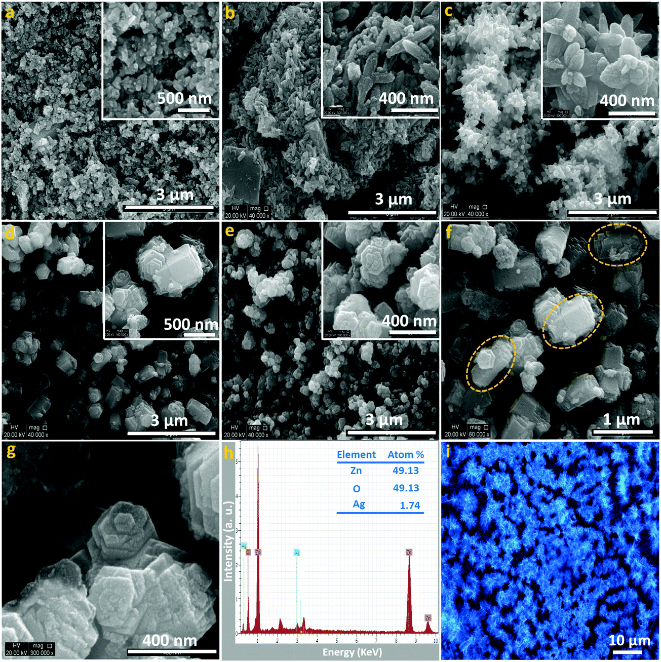 | ||
| Fig. 1 (a–e) Scanning electron micrographs of Ag/ZnO heterostructures with ZnO:Ag = 1.0:0.01, 1.0:0.013, 1.0:0.02, 1.0:0.04 and 1.0:0.1, respectively; (f) high resolution SEM image of the architectures (set D) indicating the assemblies the smaller particles, (g) high resolution SEM image of the architectures (set E) showing the tight binding of the particles, (h) energy dispersive X-ray spectrum (set C) and (i) fluorescence microscopic image of the architectures (set C) under bright field. | ||
The structural morphology of the as-synthesised heterostructures has been further confirmed by TEM, HRTEM and selected area electron diffraction patterns as shown in Fig. 2. Panel a shows the low-magnification TEM image taken from the edge of the as-prepared Ag/ZnO heterostructures (set E) which reveals that the structure is comprised of both metallic and semiconductor components. The substantially higher mass contrast sensitivity in the image causes the silver nanoparticles to appear much brighter than the surrounding ZnO architecture. The transmission electron micrographs were measured for all sets of particles; it was observed that the size of the silver particles lies in the range of 16 ± 4 nm and does not change considerably in different sets of the hererostructures. Panel b shows the HRTEM image of the Ag/ZnO heterostructures (set E) that exhibits the lattice fringes as 0.25 nm belonging to the (111) plane of fcc Ag and 0.26 nm of the (002) plane of wurtzite-type hexagonal ZnO at the edge portion, confirming the crystalline nature of Ag and ZnO components.40 The corresponding SAED pattern (panel c) of Ag/ZnO heterostructures (set E) exhibits polycrystalline-like diffraction which is consistent with the reflections (100), (002), (101), (102), (110) corresponding to the hexagonal wurtzite phase of ZnO particles along with the (111), (200) and (220) diffraction lines of Ag which reveals crystallographic orientations for both ZnO and Ag in the heterostructures.40
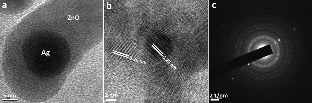 | ||
| Fig. 2 (a) Transmission electron micrograph, (b) high resolution transmission electron micrograph and (c) selected area electron diffraction pattern, corresponding to Ag/ZnO heterostructures (set E). | ||
Since microscopic analysis shows that the as-prepared microstructures are not smooth, the optical absorption of the samples has been measured by diffuse reflectance rather than by normal reflectance. Fig. 3 shows the diffuse reflectance spectra of the five different sets of Ag/ZnO microstructures in the solid state. The strong opalescence of the microstructures shows two maxima: one is in the range of 300–350 nm, which is characteristic of the ZnO direct band gap transition41 and other is near 400 nm which arises due to the localised surface plasmon absorption band of the silver nanoparticles.18 Under plasmon resonance conditions, an evanescent electric field is created on the surface of the silver nanoparticles that penetrates into the surrounding ZnO and augments the electric field of the illuminating light.25 It is seen that the positions of the maxima of both ZnO and Ag are different in the various sets, which indicates that the spatial distribution of the electrons is no more homogeneous and is modified at the interface. This is because the incorporation of silver increases the density of states impinging the photoexcited electrons of the silver nanostructures near the Fermi level of ZnO, thereby leading to the modification of the band structure at the Ag/ZnO interface.42 The efficiency of manipulation of the electromagnetic radiation, critically depends on the concentration of the metallic particles as well as the integration of plasmonic and semiconductor components within the microstructures.43 However, a regular change in the reflectance spectra was not seen with the increase in the silver nitrate concentration which can be ascribed to the interplay of different positional and orientational factors of the individual components within the Ag/ZnO microstructures.
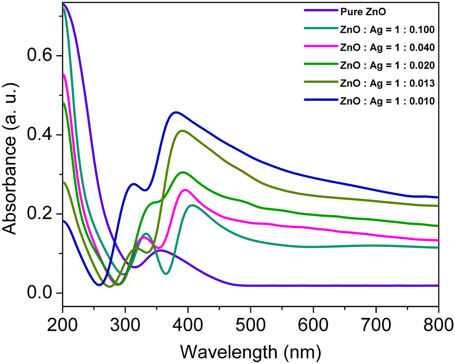 | ||
| Fig. 3 Diffuse reflectance spectra of pure ZnO and different sets of Ag/ZnO microstructures. | ||
The engineering of band gaps is common practice for exploiting semiconductors for desired physical properties.44 The electronic structure of semiconductors, such as, ZnO is characterised by a valence band, which is filled with electrons, and an empty conduction band. In metal/semiconductor microstructures, photoinduced charge carriers are trapped by the noble metal particles and become capable of promoting the interfacial charge-transfer processes.45 The optical band gap of the pure ZnO and the microstructures can be estimated using Tauc's equation, (αhν)1/n = A1/n(hν − Eg), where, α is the absorption coefficient, hν the photon energy, A a constant and Eg represents the optical bandgap. In this equation, the value of n = 1/2, for direct allowed transition. Fig. 4 shows the plot of (αhν)2 as a function of photon energy (hν) of the as-synthesised pure ZnO and five different sets of Ag/ZnO microstructures. Although the band gap of ZnO QDs has been calculated to be 3.92 eV, upon addition of silver for maneuvering Ag/ZnO microstructures, the deep level emission (DLE) band becomes significant as compared to near band edge emission (NBE) band and as a consequence, the values of the band gap are reduced to ca. 2.48, 2.45, 2.42, 2.29 and 2.19 eV with a decrease in the silver precursor concentration consistent with earlier observations.46 A significant variation in the band gap is noted due to the incorporation of silver nanostructures in the ZnO matrix. The decrease in the band gap energy could be attributed to the formation of intermediate donor levels below the conduction band, with the electron requiring less energy to move from the valence to the conduction band.47 It is, therefore, apparent that manipulating and guiding photons at the microscale inside semiconductor could, sensitively, be managed with the assistance of interdigitated plasmonic metal particles.48
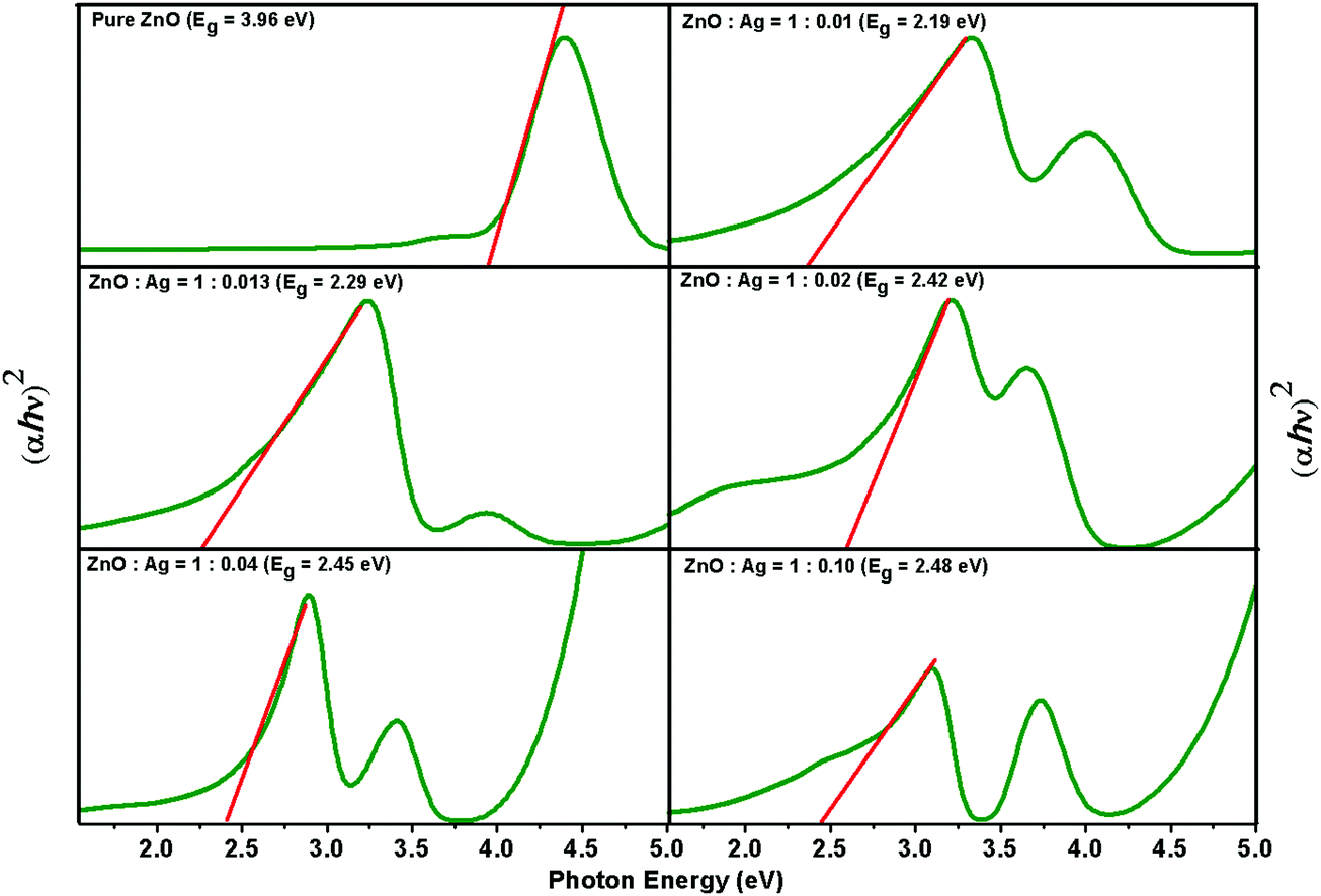 | ||
| Fig. 4 Tauc plot for the estimation of the band gap energy of pure ZnO and different sets of Ag/ZnO microstructures. | ||
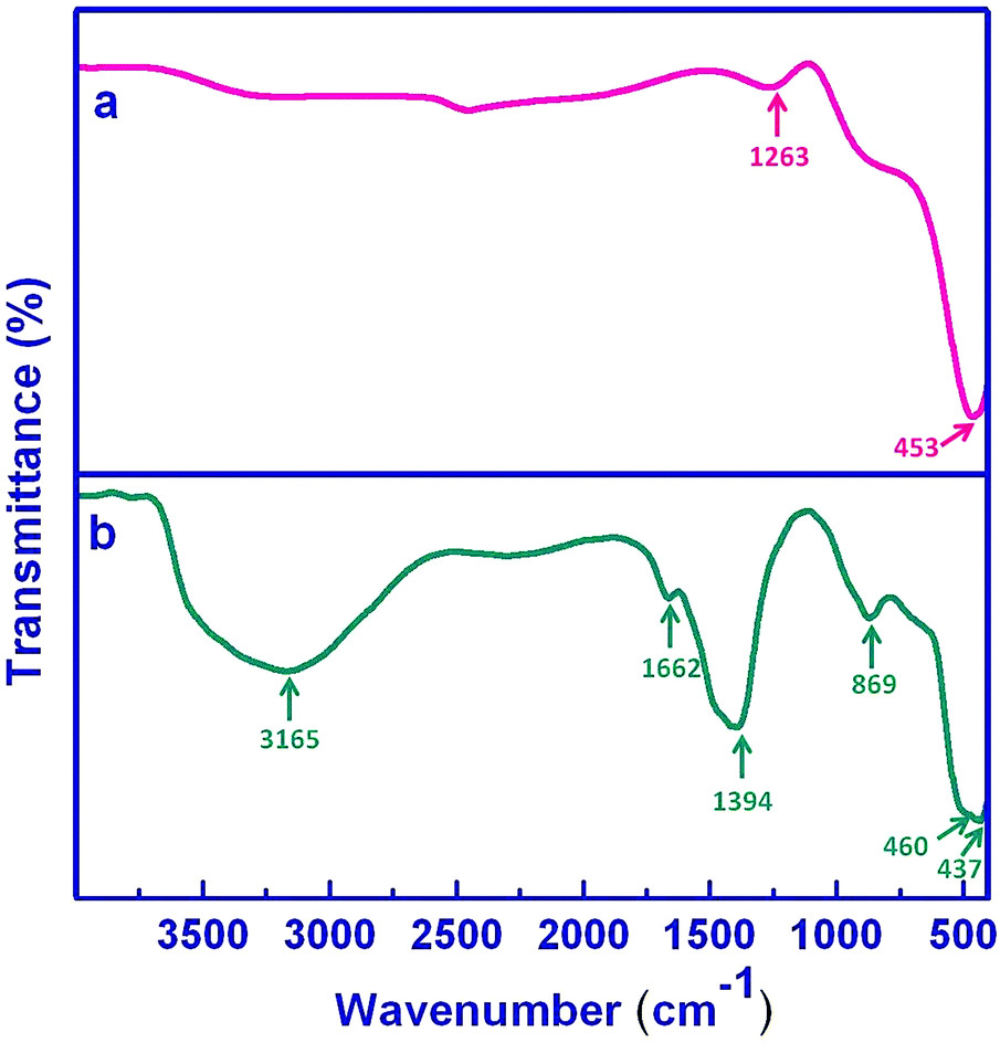
Fourier transform infrared spectra of the as-prepared pure ZnO and Ag/ZnO microstructures (set E), recorded in the range 400–4000 cm−1, are shown in Fig. 5. The FTIR spectrum of pure ZnO (trace a) shows a peak at ca. 453 cm−1 that can be assigned to stretching vibrations of Zn–O bonds; the other absorption band at 1263 cm−1 corresponds to the C–O stretching frequency due to adsorbed acetate counter ions.49 Upon addition of the silver precursor (trace b), the FTIR spectrum exhibits the appearance of two bands at ∼437 and 466 cm−1 that can be assigned to the characteristic stretching modes of Ag–O and Zn–O bonds, respectively.49 Moreover, the presence of extra bands at 1395 and 1663 cm−1 could be attributed to the asymmetric and symmetric COO− stretching vibrations of acetate chemisorption, respectively, which probably, accounts for colloid stabilisation.49 The explicit appearance of these bands in the assemblies in comparison with pure ZnO are possibly due to the large number of ZnO species present in the microstructures. The absorption bands at ca. 869 and 3165 cm−1 arise due to the stretching modes of O–H groups which reveals the existence of a small amount of water chemisorbed and/or physisorbed by the Ag/ZnO architectures.49
 | ||
| Fig. 5 Fourier transform infrared spectrum of (a) pure ZnO and (b) Ag/ZnO microstructures (set A). | ||
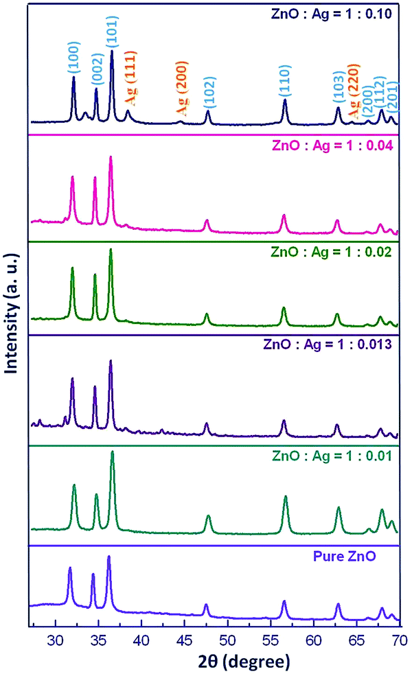
Powder X-ray diffraction patterns of the as-prepared pure ZnO and five different sets of Ag/ZnO microstructures are shown in Fig. 6. All the diffraction peaks of pure ZnO could be indexed as the pure hexagonal phase of Zn with a space group of C46v and cell constants a = 3.25 Å, and c = 5.21 Å (JCPDS: 76-0704), which suggests that the product comprises ZnO with the wurtzite structure.50 Upon addition of the silver precursor and subsequent hydrolysis in harnessing Ag/ZnO microstructures, in addition to the incipient peaks, additional diffraction peaks at ca. 38.1°, 44.3° and 64.47° (JCPDS 87-0597) corresponding to the diffraction lines of (111), (200) and (220), respectively can be indexed to the face-centred cubic structure of Ag.50 The appearance of silver peaks becomes prominent with increase in silver precursor concentration; the low intensity of the silver peaks could be attributed to an insufficient concentration of silver in the heterostructures.
 | ||
| Fig. 6 X-ray diffraction patterns of pure ZnO and different sets of Ag/ZnO microstructures. | ||
The mechanism of the emergence of morphological diversity upon increase in the silver precursor concentration has been confirmed by multiple control experiments. It has, now, been established that formation of such architectures occurs through the spatial arrangement governed by different intramolecular or intraparticulate interactions, such as electrostatic interaction, cross-linking agents, hydrogen bonding, charge transfer interaction, van der Waals forces, dipole–dipole interaction etc. amongst the individual building blocks.51 The evolution into microstructures was not seen in the absence of silver precursor; therefore, in this synthesis strategy, the in situ generated Ag seeds govern the subsequent nucleation of ZnO, which has a great influence on the final morphologies of ZnO mediated by silver ion concentration in the reaction mixture. The formation of such specific architectures is also not observed in the absence of o-xylene in the solvent medium; thus, it is apparent that the observed morphology is the result of specific interactions governed by the interfacial tension at the water–organic interface that enable effective interparticle interactions in harnessing the microstructures.52 Therefore, it could be conceived that the smaller particulates in solution with the well matched crystal lattice and active surface are prone to integrate together through the oriented attachment, driven by the increase of free energy and lattice free energy.53 The mechanism of evolution of Ag/ZnO microstructures (set E) through kinetic studies based on absorption, Fourier transform infrared and X-ray diffraction spectroscopy is enunciated in ESI3.†
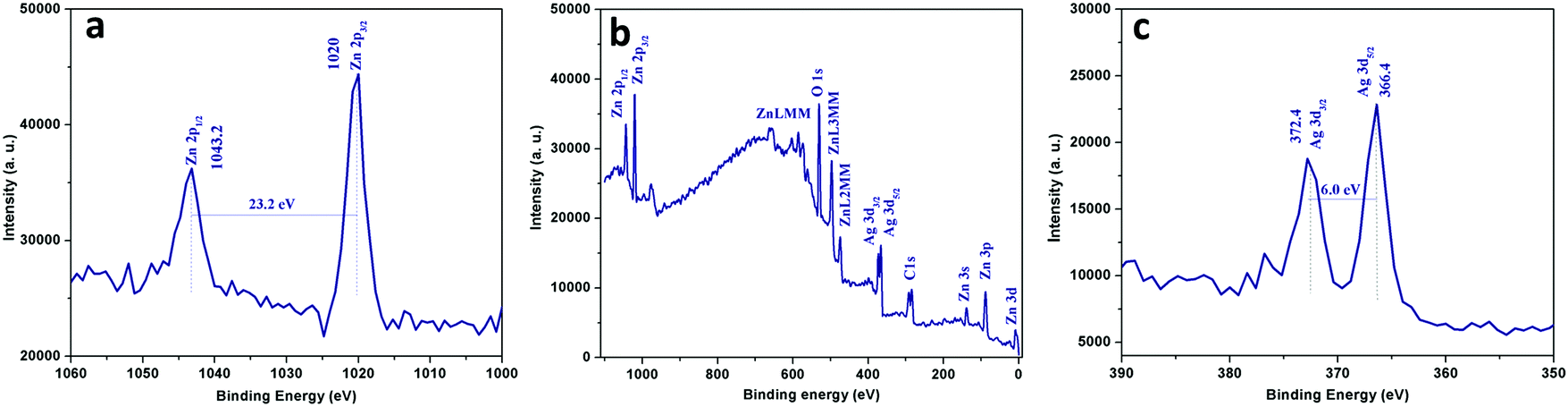
X-ray photoelectron spectroscopy analysis has been carried out for further confirmation of the purity and the composition of the Ag/ZnO microstructures (set C). The XPS spectra demonstrate the presence of Zn 2p, O 1s and Ag 3d as shown in Fig. 7. The Zn 2p (panel a) exhibits two significant binding energy peaks at 1043.2 eV (1044.4 eV in the bulk) and 1020.0 eV (1021.65 eV in the bulk) that can be attributed to 2p1/2 and 2p3/2, respectively. The splitting distance 23.2 eV between the two peaks indicates that the Zn element existed in the form of Zn2+.54 The O 1s peak (panel b) shows the position of binding energy at 532.6 eV associated with the lattice oxygen in the semiconductor matrix. Similarly, the Ag 3d (panel c) binding energy peaks are located at 372.4 (373.4 eV in bulk) and 366.4 eV (368.22 eV in the bulk) corresponding to 3d3/2 and 3d5/2, respectively. The significant shift in binding energies of Zn 2p3/2 and Ag 3d5/2 from the corresponding values of the bulk can be attributed to electron transfer from metallic Ag to ZnO crystals.55 When the metallic and semiconductor components come in contact with each other, the position of the corresponding Fermi level is equilibrated which results in excess of free electrons on the new Fermi level of the metallic components. As a consequence, the free electrons can tunnel into the vacant conduction band of the ZnO, resulting in a higher valence state of Ag components.56
 | ||
| Fig. 7 X-ray photoelectron spectra corresponding to (a) Zn 2p, (b) O 1s and (c) Ag 3d of the representative Ag/ZnO microstructures. | ||
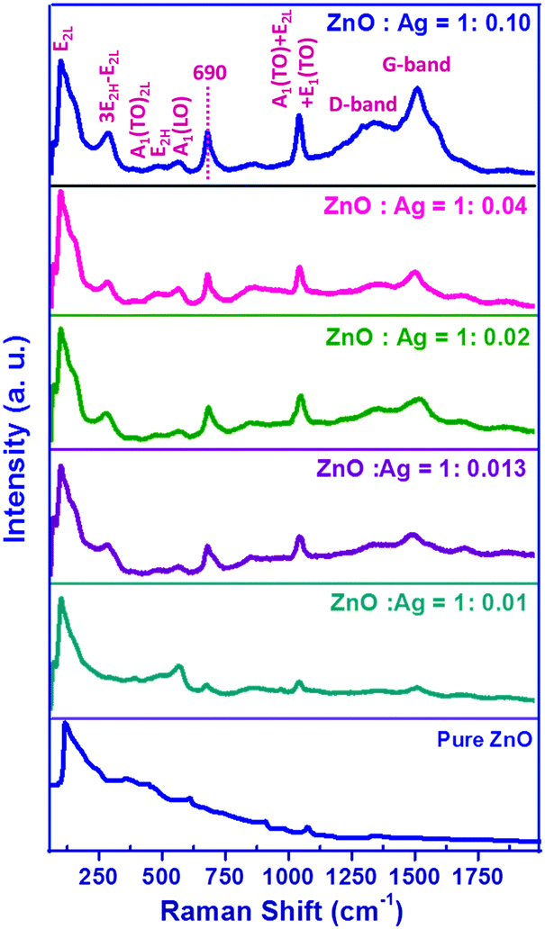
Raman spectroscopy is the most effective technique to achieve sensitive detection of optical phonon modes and therefore to characterise related vibrational properties. Fig. 8 presents the room temperature Raman spectra of pure ZnO and Ag/ZnO microstructures in the 50–2000 cm−1 spectral range; in the present experiment, the samples were excited by the 488 nm line (2.55 eV) of an Ar+˙ laser. It is seen that the spectrum of ZnO is very weak; however, the intensity of the peaks increases with increase in the silver precursor concentration; surface enhanced Raman scattering is, therefore, observed in the spectrum of Ag/ZnO microstructures. According to group theory, the structure of ZnO belongs to the C46v symmetry group having two formula units per primitive cell with all the atoms occupying the C3v sites, which predicts eight sets of zone centre optical phonons: two A1, two E1, two E2 and two B1 modes. Among these, A1 and E1 modes are polar and split into transverse (A1T and E1T) and longitudinal (A1L and E1L) phonons, all being Raman and infrared active; E2 modes are non-polar consisting of two modes of low- and high-frequency (E2L and E2H) phonons and are only Raman active, and B1 modes are infrared and Raman inactive (silent modes).29 The low frequency E2 mode is observed at 100 cm−1 which is associated with the vibration of the Zn sub-lattice while the high frequency E2 mode is related to the vibration of only oxygen atoms and is considered as the Raman fingerprint of the wurtzite ZnO phase.29 The A1(TO) and A1(LO) polar branches appeared at about 380 cm−1 and 570 cm−1, respectively; the A1(LO) phonon mode is commonly assigned to the oxygen vacancies, zinc interstitials, or defect complexes containing oxygen vacancies and zinc interstitials in ZnO.29 Other two Raman peaks located at about 331 and 1050 cm−1 can be assigned to the 3E2H–E2L and A1(TO) + E2L + E1(TO) multiphonon scattering modes, respectively.29 The Raman peak appeared at about 690 cm−1 has also been reported for co-doped ZnO; however, the origin of this peak is not yet clear.57 Nonetheless, the appearance of two new peaks at 1330 and 1581 cm−1 can be attributed to the D-band and G-band of acetate counter ions, respectively, responsible for the stabilisation of the microstructures.58 The appearance of these bands due to acetate counter ions at the higher silver concentration is in conformity with the infrared spectra as discussed earlier. The enhancement of the intensity of the Raman signal with increase in the silver precursor concentration can mainly ascribed to the interaction between the metallic and semiconductor components in the microstructures.59
 | ||
| Fig. 8 Raman spectra of pure ZnO and different sets of Ag/ZnO microstructures. | ||
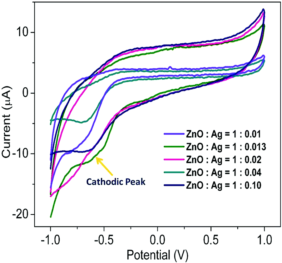
Cyclic voltammograms of five different sets of Ag/ZnO microstructures (0.01 M) in 0.1 M KCl solution using Ag/AgCl as a reference electrode and Pt electrodes as working and counter electrodes are shown in Fig. 9. It has been noted that pure ZnO shows the current values of 24.99 and 3.67 μA at the potentials of 0.45 and 0.10 V, respectively, whereas, silver nanoparticles exhibit no peak potentials in the pure state (not shown). From the spectra, it is seen that the microstructures do not possess any anodic peak potential which has been seen for pure ZnO rather a peak at Epc ∼ −0.7 V is observed with varying amount of current for different sets of Ag/ZnO microstructures. It is also noted that the amount of current is increasing (4.901, 6.557, 6.584, 8.335 and 10.385 μA for the sets of A–E, respectively) with the increasing ratio of silver in the microstructures. These results reveal that a higher number of the electrons becomes transferred from Ag to ZnO with increasing the ratio of silver in the heterostructures.49 Moreover, the differences in the flow of current are related to the differences in the extent of electron transfer at the interface of the electrodes that reflects the difference in charge densities of different sets of the microstructures.41
 | ||
| Fig. 9 Cyclic voltammograms of different sets (0.01 M) of Ag/ZnO microstructures. | ||
Due to the present state-of-the art advances in the synthesis and characterisation techniques, it has been established that plasmonic metal/semiconductor microstructures are materials of immense interest due to complementarity in the optical properties of the long-lived excitons in semiconductors and the localised electromagnetic modes in metallic nanoparticles.60 Therefore, the investigation of structure–luminescence relationship is quite fascinating in shape-selective metal/semiconductor microstructures as has been presented in Fig. 10. Panel A displays the normalised photoluminescence spectra of pure ZnO and Ag/ZnO microstructures (λex ∼ 325 nm) in the solid state. It is seen that all the photoluminescence spectra mainly consist of two types of bands: the origin of UV luminescence can be attributed to the photo-stimulated creation of excitons having energies just below the ZnO band edge and their subsequent recombination (near the band edge emission band) and the other peak in the visible region may arise from the recombination of photo-generated holes with the electrons in singly occupied oxygen vacancies (deep level emission band).14 It is seen that pure ZnO and Ag/ZnO microstructures exhibit distinctly different emission profile; specifically, the concentration of the silver precursor could tune the photoluminescence properties of the microstructures. Moreover, it is seen that near-band-edge UV luminescence is progressively shifted to the red and appearance of new bands in the visible region with increase in silver precursor concentration. Gaussian multipeak fitting in panel B explicates the evolution of two visible emission bands in the microstructures, one at 475 nm and another at 525 nm that can be attributed to the presence of oxygen vacancy states on the surface and deep interstitial oxygen states inside the microstructures.50 The change in the photoluminescence properties of ZnO as a result of the assemblage implicits the strong interaction between the semiconductor and the metallic particles and points to an efficient electron transfer from Ag to ZnO components.50
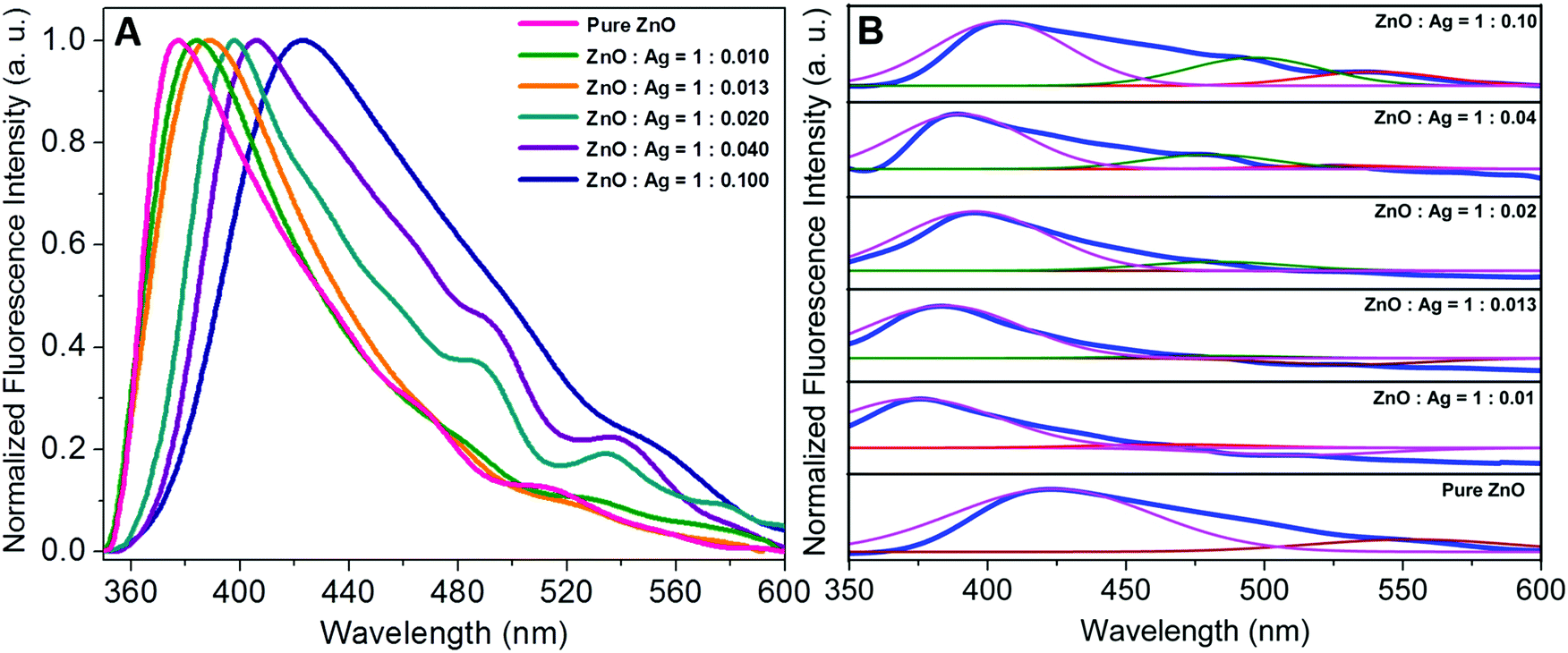 | ||
| Fig. 10 (A) Photoluminescence spectra (in the solid state) and (B) deconvolution of the spectra of pure ZnO and different sets of ZnO–Ag microstructures. | ||
The work function of a semiconductor can be represented as Δϕ = I + Vbb − (EF − EV) = χ + Vbb + (EC − EF), where Vbb is the band bending, χ the electron affinity, I the ionization energy, and EC and EV are the band energies of the conduction and valence bands in the bulk.61 With increase in silver deposition around the ZnO surface, the dipole causes a change in electron affinity or the ionization energy and space charge diffusion cause the change in the band bending potential. Considering the change in band bending, the shift in Fermi energy level (EF) takes the major contribution, which again depends on the dopant characteristics. When the metallic Ag and semiconducting ZnO species are in contact with each other, the position of the corresponding Fermi levels of both the species are equilibrated and as a consequence there is an excess of free electrons in the new Fermi level of metallic Ag components.62–64 Under such a situation, because the conduction band of the ZnO species is vacant, the free electrons can tunnel into the conduction band that results in a higher valence state of metallic Ag components resulting in a Schottky junction as illustrated in Scheme 1. Chernysheva et al. have shown the shift in Fermi level of ZnO by ∼0.04 eV on the Ag/ZnO contact.65 The work functions for Ag (ΦM = 4.26 eV) and ZnO (ΦS = 5.2 eV) have been adopted from the reference of Zheng et al.56 where V0 defines the defect level and Eg the band gap of the semiconductor layer. Adsorbates modify the ionization energy and induce a change in band bending for a perfect Schottky contact (where, ΦSB is the Schottky barrier of the interface), and construct the interface levels, from which the transition can be shown.65 The change in the ionization energy with the increasing concentration of Ag on ZnO can be expressed as ΔI = Δχ = eNp⊥(θ)/ε0, where, e is the electronic charge, N the number of dipoles and p⊥(θ) the perpendicular polarisation through the adsorbate layer. Thus, with the increase in the Ag concentration around ZnO, both of the effects lead to the decrease the difference in valence and conduction bands. Therefore, with increase in silver concentration around ZnO, there occurs a successive red shift in photoluminescence spectra.29,61,65
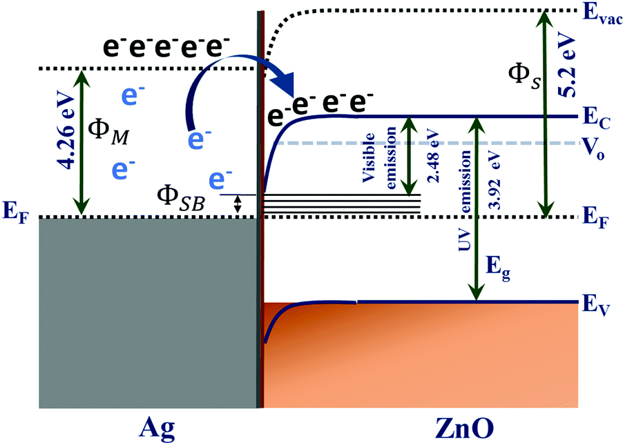 | ||
| Scheme 1 Schematic presentation of the energy profile showing the electron transfer processes at the Ag/ZnO microstructures. | ||
We have attempted to calculate the distribution of electric field corresponding to a single silver nanoparticle in the assemblies through a finite element method. A representative schematic presentation for the calculation and the corresponding electric field distribution pattern are exhibited in Fig. 11. Plane polarised electromagnetic waves were passed through the linear arrangement assuming a concentric spherical shell around the metallic core (panel a) in the corresponding transmission electron micrograph (set B). The maximum electric field has been located along the E-field polarisation direction (y-axis) as shown in the inset. The dielectric constants for ZnO66 and Ag67 were taken as 8.5 and 2.56, respectively in this calculation. It is observed that the electric field intensity on the outer ZnO surface is stronger than that of the Ag (panel b). Moreover, it is noted that the enhanced local field polarises parallel to the incident polarization and concentrates on the outer surface in the ZnO shell with the maximum |E2| as ca. 8.4 eV. This can be ascribed to the presence of plasmonic field of nanostructured metallic particles to the ZnO shell across the interface. However, since many metal nanoparticles are embedded in the giant semiconductor matrix, the exact calculation of electric field throughout the entire microstructure warrants the modification of mathematical formulation considering the electromagnetic coupling effect in adjacent metallic nanostructures which is the subject of further investigation.11,68,69
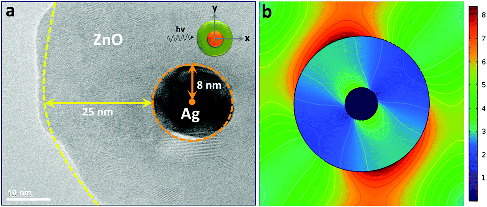 | ||
| Fig. 11 (a) Representative transmission electron micrograph (set B) for parametric assignment and (b) calculation of electric field corresponding to single silver nanoparticles in Ag/ZnO microstructures through the finite element method. Inset in panel (a) shows the polarisation direction of the incident light. | ||
4. Conclusions
In conclusion, we have elucidated the spectral properties due to interfacial interactions between plasmonic metal nanoparticles embedded in a giant semiconductor matrix. The reported synthetic strategy based on colloidal chemistry provides a facile route to the effective integration of plasmonic metal/semiconductor microstructures under a unified synthetic protocol. It has been seen that with increase in silver precursor concentration, the ease and specificity of this dual-solvent thermolytic method provides a rational approach for the synthesis of diverse microstructures. It has been resolved that the in situ nucleation and growth of the Ag domains followed by heterogeneous nucleation and growth of the ZnO component controls their spatial arrangement to induce a unique morphology with dimensions on the microscale. Spectral characterisations elucidate interfacial electron transfer at the Ag/ZnO interface in the microstructures. Such heterogeneous microstructures present not only numerous natural interfaces for integrating multiple functions but also exhibit a substantial reduction in the band gap that may lead to the emergence of new properties and functions. The combination of metal and semiconductor renders the emergence of complementary optoelectronic properties that can be employed in potential technological applications in physics, chemistry, biology and medicine. Because many metal nanoparticles are embedded in single giant semiconductor architecture, these microstructures provide new model systems for the modification of respective theoretical models with many body interfacial electron transfer processes. Therefore, the findings of this research will help in developing a strategy that is capable of producing micro/nanostructures with the desired geometric features and specific functionalities.Conflicts of interest
There are no conflicts to declare.Acknowledgements
We gratefully acknowledge financial support from DST-SERB, New Delhi (Project No.: EMR/2016/006842). We are grateful to Prof. Yuichi Negishi, Tokyo University of Science, Shinjuku-ku, Japan, for providing support to X-ray Photoelectron Spectroscopy measurements.References
- Z. Zhang and J. T. Yates, Chem. Rev., 2012, 112, 5520–5551 CrossRef CAS.
- H. Harutyunyan, A. B. F. Martinson, D. Rosenmann, L. K. Khorashad, L. V. Besteiro, A. O. Govorov and G. P. Wiederrecht, Nat. Nanotechnol., 2015, 10, 770–774 CrossRef CAS.
- S. K. Cushing, J. Li, J. Bright, B. T. Yost, P. Zheng, A. D. Bristow and N. Wu, J. Phys. Chem. C, 2015, 119, 16239–16244 CrossRef CAS.
- T. Tatsuma, H. Nishi and T. Ishida, Chem. Sci., 2017, 8, 3325–3337 RSC.
- W. Schottky, Z. Phys., 1939, 113, 367–414 CrossRef CAS.
- A. O. Govorov, H. Zhang, H. V. Demir and Y. K. Gun’ko, Nano Today, 2014, 9, 85–101 CrossRef CAS.
- S. K. Ghosh and T. Pal, Chem. Rev., 2007, 107, 4797–4862 CrossRef CAS.
- C. Voisin, D. Christofilos, P. A. Loukakos, N. Del Fatti, F. Vallée, J. Lermé, M. Gaudry, E. Cottancin, M. Pellarin and M. Broyer, Phys. Rev. B: Condens. Matter Mater. Phys., 2004, 69, 195416 CrossRef.
- A. M. Brown, R. Sundararaman, P. Narang, W. A. Goddard III and H. A. Atwater, ACS Nano, 2016, 10, 957–966 CrossRef CAS.
- S. Link and M. A. El-Sayed, Int. Rev. Phys. Chem., 2010, 19, 409–453 Search PubMed.
- E. Blandre, D. Jalas, A. Petrov and M. Eich, ACS Photonics, 2018, 5, 3613–3620 Search PubMed.
- W. Li and J. G. Valentine, Nanophotonics, 2017, 6, 177–191 Search PubMed.
- B. A. Korgel, Nat. Mater., 2007, 6, 551–552 CrossRef CAS.
- U. Banin, Y. Ben-Shahar and K. Vinokurov, Chem. Mater., 2014, 26, 97–110 CrossRef CAS.
- R. Jiang, B. Li, C. Fang and J. Wang, Adv. Mater., 2014, 26, 5274–5309 CrossRef CAS.
- Z. L. Wang, Mater. Today, 2004, 7, 26–33 CrossRef CAS.
- C. Klingshirn, Chem. Phys. Chem., 2007, 8, 782–803 CrossRef CAS.
- X. Liu, D. Li, X. Sun, Z. Li, H. Song, H. Jiang and Y. Chen, Sci. Rep., 2015, 5, 12555 CrossRef CAS.
- Y. Li, X. Zhao and W. Fan, J. Phys. Chem. C, 2011, 115, 3552–3557 CrossRef CAS.
- O. Volnianska, P. Boguslawski, J. Kaczkowski, P. Jakubas, A. Jezierski and E. Kaminska, Phys. Rev. B: Condens. Matter Mater. Phys., 2009, 80, 245212 CrossRef.
- T.-J. Whang, M.-T. Hsieh and H.-H. Chen, Appl. Surf. Sci., 2012, 258, 2796–2801 CrossRef CAS.
- Y. Yan, M. M. Al-Jassim and S. H. Wei, Appl. Phys. Lett., 2006, 89, 181912 CrossRef.
- M. He, Y. Tian, D. Springer, I. Putra, G. Xing, E. Chia, S. Cheong and T. Wu, Appl. Phys. Lett., 2011, 99, 222511 CrossRef.
- B. P. Khanal, A. Pandey, L. Li, Q. Lin, W. K. Bae, H. Luo, V. I. Klimov and J. M. Pietryga, ACS Nano, 2012, 6, 3832–3840 CrossRef CAS.
- J. Wei, N. Jiang, J. Xu, X. Bai and J. Liu, Nano Lett., 2015, 15, 5926–5931 CrossRef CAS.
- T. N. Q. Trang, T. B. Phan, N. D. Nam and V. T. H. Thu, ACS Appl. Mater. Interfaces, 2020, 12, 12195–12206 CrossRef CAS.
- R. Wang, W. Yang, Y. Song, X. Shen, J. Wang, X. Zhong, S. Li and Y. Song, Sci. Rep., 2015, 5, 9189 CrossRef.
- E. J. Guidelli, O. Baffa and D. R. Clarke, Sci. Rep., 2015, 5, 14004 CrossRef CAS.
- R. Sánchez Zeferino, M. Barboza Flores and U. Pal, J. Appl. Phys., 2011, 109, 014308 CrossRef.
- J. K. Hyun, T. Kang, H. Baek, H. Oh, D.-S. Kim and G.-C. Yi, ACS Photonics, 2015, 2, 1314–1319 CrossRef CAS.
- A. Kim, Y. Won, K. Woo, C.-H. Kim and J. Moon, ACS Nano, 2013, 7, 1081–1091 CrossRef CAS.
- H. Y. Jun, C.-H. Chang, K.-S. Ahn, S. O. Ryu and C.-H. Choi, CrystEngComm, 2020, 22, 646–653 RSC.
- H. R. Liu, G. X. Shao, Z. F. Zhao, Z. X. Zhang, Y. Zhang, X. Liang, X. G. Liu, H. S. Jia and B. S. Xu, J. Phys. Chem. C, 2012, 116, 16182–16190 CrossRef CAS.
- J. Manna, S. Goswami, N. Shilpa, N. Sahu and R. K. Rana, ACS Appl. Mater. Interfaces, 2015, 7, 8076–8082 CrossRef CAS.
- M. Zare, K. Namratha, S. Alghamdi, Y. H. E. Mohammad, A. Hezam, M. Zare, Q. A. Drmosh, K. Byrappa, B. N. Chandrashekar, S. Ramakrishna and X. Zhang, Sci. Rep., 2019, 9, 8303 CrossRef.
- C. Pacholski, A. Kornowski and H. Weller, Angew. Chem., Int. Ed., 2002, 41, 1188–1191 CrossRef CAS.
- Z. Zheng, Z. S. Lim, Y. Peng, L. You, L. Chen and J. Wang, Sci. Rep., 2013, 3, 2434 CrossRef.
- F.-R. Fan, Y. Ding, D.-Y. Liu, Z.-Q. Tian and Z. L. Wang, J. Am. Chem. Soc., 2009, 131, 12036–12037 Search PubMed.
- M. Ali, S. K. Pal, H. Rahaman and S. K. Ghosh, Soft Matter, 2014, 10, 2767–2774 RSC.
- H. R. Liu, Y. Hu, Z. Zhang, X. Liu, H. Jia and B. Xu, Appl. Surf. Sci., 2015, 07, 644–652 CrossRef.
- M. L. Kahn, T. Cardinal, B. Bousquet, M. Monge, V. Jubera and B. Chaudret, Chem. Phys. Chem., 2006, 7, 2392–2397 CrossRef CAS.
- X. Chen, Y. Li, X. Pan, D. Cortie, X. Huang and Z. Yi, Nat. Commun., 2016, 7, 12273 CrossRef CAS.
- M. Achermann, J. Phys. Chem. Lett., 2010, 1, 2837–2843 CrossRef CAS.
- F. Wu, L. Tian, R. Kanjolia, S. Singamaneni and P. Banerjee, ACS Appl. Mater. Interfaces, 2013, 5, 7693–7697 CrossRef CAS.
- S. K. Dutta, S. K. Mehetor and N. Pradhan, J. Phys. Chem. Lett., 2015, 6, 936–944 CrossRef CAS.
- Y. Dong, C. Feng, P. Jiang, G. Wang, K. Li and H. Miao, RSC Adv., 2014, 4, 7340–7346 RSC.
- R. T. Tung, Appl. Phys. Rev., 2014, 1, 011304 Search PubMed.
- S. Lu, J. Qi, S. Liu, Z. Zhang, Z. Wang, P. Lin, Q. Liao, Q. Liang and Y. Zhang, ACS Appl. Mater. Interfaces, 2014, 6, 14116–14122 CrossRef CAS.
- J. Huang, Z. Yang, Z. Feng, X. Xie and X. Wen, Sci. Rep., 2016, 6, 24471 CrossRef CAS.
- M. E. Aguirre, H. B. Rodríguez, E. S. Román, A. Feldhoff and M. A. Grela, J. Phys. Chem. C, 2011, 115, 24967–24974 CrossRef CAS.
- Y. Min, M. Akbulut, K. Kristiansen, Y. Golan and J. Israelachvili, Nat. Mater., 2008, 7, 527–538 CrossRef CAS.
- R. B. Grubbs, Nat. Mater., 2007, 6, 553–555 CrossRef CAS.
- X. Yan, Z. Li, C. Zou, S. Li, J. Yang, R. Chen, J. Han and W. Gao, J. Phys. Chem. C, 2010, 114, 1436–1443 CrossRef CAS.
- Y. Liang, N. Guo, L. Li, R. Li, G. Ji and S. Gan, New J. Chem., 2016, 40, 1587–1594 RSC.
- P. Fageria, S. Gangopadhyay and S. Pande, RSC Adv., 2014, 4, 24962–24972 RSC.
- Y. Zheng, L. Zheng, Y. Zhan, X. Lin, Q. Zheng and K. Wei, Inorg. Chem., 2007, 46, 6980–6986 CrossRef CAS.
- N. Hasuike, R. Deguchi, H. Katoh, K. Kisoda, K. Nishio, T. Isshiki and H. Harima, J. Phys.: Condens. Matter, 2007, 19, 3652231 CrossRef.
- J.-C. Valmalette, Z. Tan, H. Abe and S. Ohara, Sci. Rep., 2014, 4, 5238 CrossRef CAS.
- Y. Xie, S. Yang, Z. Mao, P. Li, C. Zhao, Z. Cohick, P.-H. Huang and T. J. Huang, ACS Nano, 2014, 8, 12175–12184 CrossRef CAS.
- Y. Yin, Y. Sun, M. Yu, X. Liu, T. Jiang, B. Yang, D. Liu, S. Liu and W. Cao, Sci. Rep., 2015, 5, 8152 CrossRef CAS.
- A. B. Djurisic, W. C. H. Choy, V. A. L. Roy, Y. H. Leung, C. Y. Kwong, K. W. Cheah, T. K. GunduRao, W. K. Chan, F. Lui and C. Surya, Adv. Funct. Mater., 2004, 14, 856–864 CrossRef CAS.
- S. Wang, F. Jia, X. Wang, L. Hu, Y. Sun, G. Yin, T. Zhou, Z. Feng, P. Kumar and B. Liu, ACS Omega, 2020, 5, 5209–5218 CrossRef CAS.
- M. D. L. R. Peralta, U. Pal and S. R. Zeferino, ACS Appl. Mater. Interfaces, 2012, 4, 4807–4816 CrossRef.
- Y. Yao, F. Ji, M. Yin, X. Ren, Q. Ma, J. Yan and S. F. Liu, ACS Appl. Mater. Interfaces, 2016, 8, 18165–18172 CrossRef CAS.
- E. Chernysheva, W. Srour, B. Philippe, B. Baris, S. Chenot, R. F. Duarte, M. Gorgoi, H. Cruguel, H. Rensmo, H. Montigaud, J. Jupille, G. Cabailh, S. Grachev and R. Lazzari, Phys. Rev. B, 2018, 97, 235430 CrossRef CAS.
- https://www.efunda.com/materials/piezo/material_data/matdata_output.cfm?Material .
- K. Imazu, A. Yoshida, D. Tanaka and K. Tamada, SpringerPlus, 2014, 3, 284 CrossRef.
- R. H. Fowler, Phys. Rev., 1931, 38, 45–56 CrossRef CAS.
- Y. Hattori, T. Taniguchi, K. Watanabe and K. Nagashio, ACS Appl. Mater. Interfaces, 2018, 10, 11732–11738 CrossRef CAS.
Footnote |
| † Electronic supplementary information (ESI) available. See DOI: 10.1039/d0ma00362j |
| This journal is © The Royal Society of Chemistry 2020 |