
 Open Access Article
 This Open Access Article is licensed under a Creative Commons Attribution-Non Commercial 3.0 Unported Licence
Extended topological line defects in graphene for individual identification of DNA nucleobases†
Rameshwar L.
Kumawat
 a and
Biswarup
Pathak
*ab
a and
Biswarup
Pathak
*ab
aDiscipline of Metallurgy Engineering and Materials Science, School of Basic Sciences, Indian Institute of Technology (IIT) Indore, Indore, Madhya Pradesh 453552, India. E-mail: biswarup@iiti.ac.in
bDiscipline of Chemistry, School of Basic Sciences, Indian Institute of Technology (IIT) Indore, Indore, Madhya Pradesh 453552, India
First published on 14th October 2020
Abstract
Recently synthesized topological line defects in graphene containing octagonal and a pair of pentagonal structures open up new research directions for nano-sized electronic device applications. In this study, using consistent-exchange van der Waals density functional (vdW-DF-cx) calculations, we investigated an extended line defects (ELDs)-based graphene nano-device for individual identification of all four DNA nucleobases. The electronic transport properties of the ELDs in graphene and the conductance caused by adsorption of all four nucleobases on the ELDs in graphene were investigated to understand the capability for individual identification of all four DNA nucleobases using the non-equilibrium Green's function (NEGF) method. Our results show that the π–π interaction is very much responsible for the Fano resonance characteristics and such an ELDs graphene-based nano-device may detect the four nucleobases better than a graphene-based nano-device without line defects. Also, the results of the I–V characteristics indicate that a specific voltage window is required for individual identification of all four nucleobases. Thus, we believe that a one-dimensional ELDs graphene-based nano-device is promising for DNA sequencing.
1. Introduction
Nano-electronics based techniques have been found to be very promising for next-generation DNA sequencing.1–20 Theoretical and experimental attempts have been made to model nanochannel-,14–19 nanopore-,1–8,20–26 and nanogap-12,27–33 based nano-electronic devices for DNA sequencing. Such nanogap/pore-based devices, through which single-strand DNA (ssDNA) can be translocated, were identified as a low-cost technique to sequence the whole genome.1–8,20–34 Therefore, the development of fast and controlled DNA sequencing methods has progressed much over the past decades. However, DNA sequencing through a gap/pore could be challenging due to various issues. Controlling the DNA nucleotide translocation speed, suppressing stochastic nucleotide motions, and determining the signal overlaps between different nucleotides are some of the major problems for the developing gap/pore-based DNA sequencing techniques to achieve single-nucleobase resolution at the molecular level.21,22,34 Therefore, it would be useful to develop a nano-sized device that could hold each nucleobase firmly while the nucleobase is being identified.14,17–19Understanding the interactions of DNA nucleobases with the inert surfaces of low-dimensional materials is a theme of interest because of its importance for single-molecule detection.1,14,17,18,35–37 Indeed, both experimental and theoretical reports of the adsorption of DNA nucleobases on two-dimensional (2D) and one-dimensional (1D) surfaces have been explored for this purpose.14–19,38–43 Such works have been done to understand the binding strength, adsorption and desorption processes, and binding mechanisms of the nucleobases.19,44 So far, several 2D and 1D materials have been proposed for nucleobase recognition, including graphene,14–18,35–43 silicene,44 boron nitride (BN),18,45 phosphorene,19 dichalcogenides,24 and so on. Such studies allow the scientific community to understand the nature of the interaction, which is helpful for the molecular recognition process. Moreover, the interactions of nucleobase molecules with 2D and 1D graphene surfaces have been extensively studied.14–18,35–43 For example, Kim et al. theoretically demonstrated the possibility of four-nucleobase detection using an ultrafast and highly sensitive graphene nanoribbon (GNR)-embedded nanochannel device that can electrically distinguish all four nucleobases.14–18 They claimed that such a nano-sized device can effectively control the motion of DNA nucleobases through π–π interaction and can decipher the highly sensitive characteristic Fano resonance driven conductance of each nucleobase. Further, in 2014, Thomas et al. theoretically demonstrated that individual nucleobase detection could be possible through conductance measurements using narrow size semiconducting based nanoribbons (graphene, MoS2, silicene, and hexagonal BN) which give dips in the conductance curve when stacked with the nucleobases.18 Similarly, Amorim et al. computationally designed a 2D silicene-based device that could be used as an electrical biosensor.44
Furthermore, Heerema et al. revealed that the adsorption of DNA nucleobases on highly sensitive GNR is very helpful in collecting DNA-nucleobase-specific information.4 Moreover, fluctuation (position/angles) of the DNA nucleobases is minimized, which in turn lowers the noise. Therefore, all these studies establish that the adsorption phenomenon is very promising for the detection of DNA nucleobases. While low dimensional materials have been found to be promising for such applications, a key factor in single-molecule recognition remains challenging: a low signal to noise ratio.26,27,31–34,46,47 This, in fact, has hindered device fabrication with such materials for their practical use in DNA sequencing.48 Graphene combines the features of an atomically thin membrane with strong carbon–carbon (C–C) bonds.49,50 However, scientists/researchers are continually searching for comparatively more sensitive materials for DNA sequencing applications.
In this regard, extended line defects (ELDs), like grain boundaries in graphene, formed by a combination of octagons and pentagons (o–p) can improve the sensitivity of graphene.51–53 Lahiri and co-workers have synthesized 1D extended topological defect lines in graphene, containing octagonal and paired pentagonal sp2-hybridized C rings.51 The recent synthesis of such extended 1D topological line defects in a graphene sheet gives the possibility of the fabrication of graphene-based devices with line defects that can be utilized as quasi-1D metallic nanowire-based nano-device structures.51,54,55 Furthermore, such ELDs induce charge redistribution in their surroundings.51,54 These ELDs act as conducting quasi-1D metallic wires embedded in a graphene sheet.51 Certainly, reducing the dimensionality is a promising path towards improving sensitivity. Moreover, the perfectly defined atomic structure of the o–p line defect embedded in a thick graphene sheet may help to practically solve one of the significant tasks of nano-electronics: the realization of precisely controlled contacts at the atomic level.51 This is immediately required for the advance of molecular nano-electronics and single-molecule sensing nano-devices. Such ELDs may truly improve the sensitivity and quantum transport properties of the graphene-based device. Therefore, it would be interesting to understand the conductance properties when each nucleobase is π-stacked to the ELDs in the graphene sheet (ELDs graphene). Moreover, the π–π interaction must be adequately robust to sustain the stacking structures for conductance and current (I) measurements, while being weak enough to permit the ssDNA to be translocated by an external driving force.
Motivated by all these reports, we introduce ELDs into a graphene sheet to improve the performance of the ELDs graphene-based nano-sized DNA nucleobase sensors. This proposed ELDs graphene device will interact with each nucleobase through π–π interaction. In this work, we use first-principles based density functional theory (DFT) calculations to investigate the structural, adsorption, and electronic properties of the ELDs graphene and ELDs graphene + nucleobase systems. Further, the electronic transport properties of the ELDs graphene and the electric conductance caused by adsorption of all four nucleobase molecules on the ELDs graphene were examined to understand its capability for individual identification of all four DNA nucleobases. We compute the zero-bias transmission function [T(E)], conductance sensitivity (S%), and current–voltage (I–V) characteristics of the ELDs graphene + nucleobase systems using a combination of DFT with a non-equilibrium Green's functions (NEGF) approach.
2. Model and computational methods
The atomic structure of the extended topological 1D line defects in graphene considered in this work is shown in Fig. 1. It consists of a graphene device containing octagonal and paired pentagonal line defects extending along the entire setup in the transport direction. The ELDs graphene device is periodic in the x- and z-directions, as shown in Fig. 1. We considered all four DNA nucleobases on the ELDs graphene device for our calculations. The four nucleobases are adenine (A), guanine (G), thymine (T), and cytosine (C).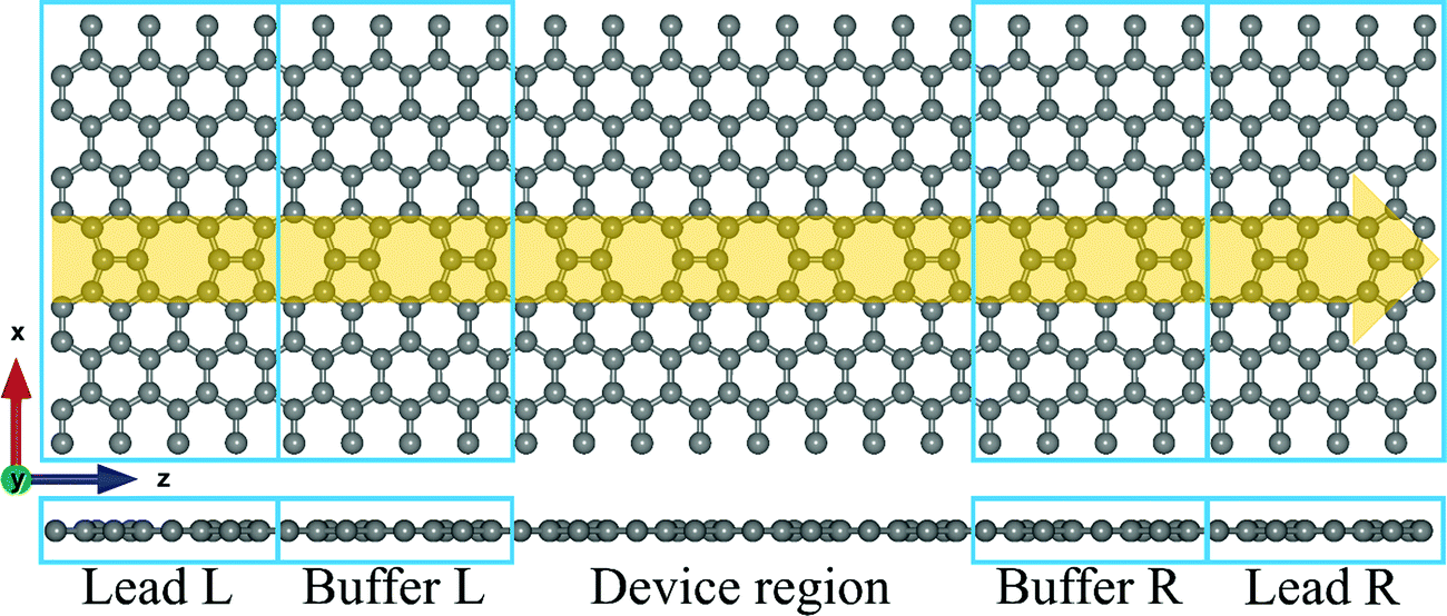 | ||
| Fig. 1 Schematic view of the modelled ELDs graphene nano-sized device (top and side views) consisting of two semi-infinite leads [left (L) and right (R)], buffer region, and the device region. Atom color code: C (grey). | ||
First, we investigated the adsorption phenomenon of all four DNA nucleobases on ELDs graphene. For the calculations, we consider a single nucleobase at a time on the ELDs graphene. First, we relaxed the isolated nucleobase molecules using the B3LYP/6-311++G** basis sets as implemented in Gaussian 09 code.56 Taking the relaxed geometries of the nucleobase molecules, we adsorbed each nucleobase molecule on the surface of the ELDs graphene. After that, all the ELDs graphene + nucleobase system configurations were fully optimized using the GGA-PBE method as implemented in the SIESTA code.57–59 We used the GGA-PBE for exchange and correlation functionals, in which valence electrons are described using the double-ζ polarized basis sets for all atoms.59 The consistent-exchange van der Waals density functional (vdW-DF-cx) method implemented in the SIESTA code was used to treat the weak dispersion interaction.60 Troullier–Martins norm-conserving pseudopotentials were used to model the atomic core electrons.61 We employed a Monkhorst k-space grid of 5 × 1 × 3 and a mesh cut-off energy value of 200 Ry. For all the systems, a vacuum distance of 32 Å was used, which is sufficient to avoid spurious interactions between repeated images.
The adsorption energies (Eads) are calculated on the ELDs graphene surface using the following equation
| Eads = [EELDs graphene+nucleobase − (Enucleobase + EELDs graphene)] | (1) |
The electronic charge density difference (Δρ(r)) is plotted to understand the nature of the interaction for all four DNA nucleobases on the ELD graphene surface and is calculated using the following equation
Δρ(r) = [ρELDs![[thin space (1/6-em)]](https://www.rsc.org/images/entities/char_2009.gif) graphene+nucleobase(r) − (ρELDsgraphene(r) + ρnucleobase(r))] graphene+nucleobase(r) − (ρELDsgraphene(r) + ρnucleobase(r))] | (2) |
graphene+nucleobase(r) represents the total charge density on the ELDs graphene surface in the presence of an adsorbed DNA nucleobase molecule, ρELDsgraphene(r) is the charge density on the isolated ELDs graphene surface, and ρnucleobase(r) is the charge density of the isolated DNA nucleobase molecule.
The first principles DFT calculation is combined with the NEGF approach to obtain the electronic transport properties by employing the TranSIESTA code.57,62 The electronic transport properties are based on the Landauer–Büttiker approach. The schematic of the proposed transport setup is shown in Fig. 1. It consists of left and right leads, buffer regions, and a central scattering region (device region). The basis sets used in the electronic transport calculation are the same as those used in the optimization and 8 × 1 × 1 k-points are used to define the real-space-grid. Further, the T(E) and I–V characteristics are calculated by considering only the gamma-centered k-points for Brillouin zone sampling employing the TBTrans code.62 The T(E) is calculated using the equation
 | (3) |
 and the NEGFs for the device region are defined as
  , where Ss is the overlap-matrix and Hs is the Hamiltonian-matrix, ΣL/R = VSL/RgL/RVL/Rs is the self-interaction energy, ΣL/R is a lead (electrode) that takes into account the L/R leads onto the device region, gL/R is the surface Green's function (L/R) and
  is the coupling-matrix between the leads (L/R) and the device region.62
Moreover, the integration of T(E) delivers the electric current (I) given by the equation
 | (4) |
3. Results and discussion
3.1. ELDs graphene device
The optimized geometry of the line defect structure, with bond angles (°) and bond lengths (Å), is shown in Fig. 2a. Fig. 2a shows the topological line defect graphene sheet consisting of a pair of pentagonals (p) and one octagonal (o), which is periodically repeated along the dislocation line. In this geometry, the bond lengths (∼1.39 to 1.46 Å) and bond angles (112 to 136°) are similar to those of sp2 hybridized carbon.51Fig. 2b shows the T(E) and density of states (DOS) of the ELDs graphene device. The ELDs graphene has a step-like transmission curve because of the gamma point calculation. Further, the transmission curve indicates that there are several conducting channels available for transport around the Fermi-level. Both the T(E) and DOS results show that ELDs graphene can work as a metallic nanowire embedded in the graphene sheet. Considering the outcomes above, we turn our attention to the use of this potential nano-device for DNA sequencing applications.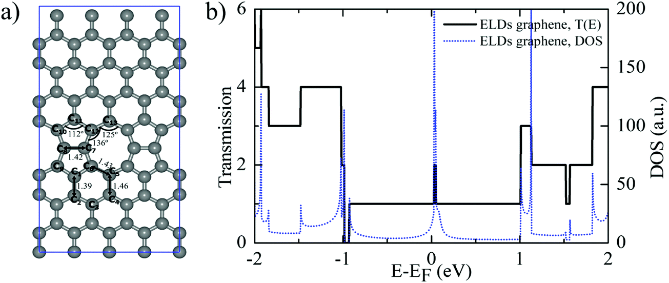 | ||
| Fig. 2 (a) The relaxed geometry of the defected structure with bond lengths (Å) and bond angles (°). (b) The electronic T(E) and DOS characteristics of the ELDs graphene device. | ||
3.2. Physisorption of nucleobases
We studied the adsorption behavior of all four nucleobase molecules (A, G, T, and C) on the ELDs graphene sheet. For this, we systematically studied the adsorption phenomenon of all four nucleobase molecules at five different possible adsorption sites (A1, A2, A3, A4, and A5) on the ELDs graphene sheet, as shown in Fig. S1 [ESI†]. The initial distance between the nucleobase and the sheet was kept at around 2.8 Å. The center of the hexagonal ring of each DNA nucleobase molecule is positioned on the hollow [octagon (A1), pentagon (A2), hexagon (A4)] and bridge [pentagon–octagon (A3) and octagon–hexagon (A5)] sites of the ELDs graphene sheet as shown in Fig. S2 and S3 (ESI†). Fig. S2 and S3 (ESI†) shows the initial (before optimization) and final configurations (after optimization) for all four nucleobases on the ELDs graphene sheet. We find that all four nucleobases slightly shift from their original (initial) position after optimization. The computed relative energy values are shown in Table S1 (ESI†). The A3 configuration [bridge site (pentagon–octagon)] is the most energetically stable adsorption site for the A nucleobase, whereas the G, T, and C nucleobases prefer to adsorb at the A5 site [bridge site (octagon–hexagon)]. The most energetically stable configurations of all four nucleobases are shown in Fig. 3(a–d).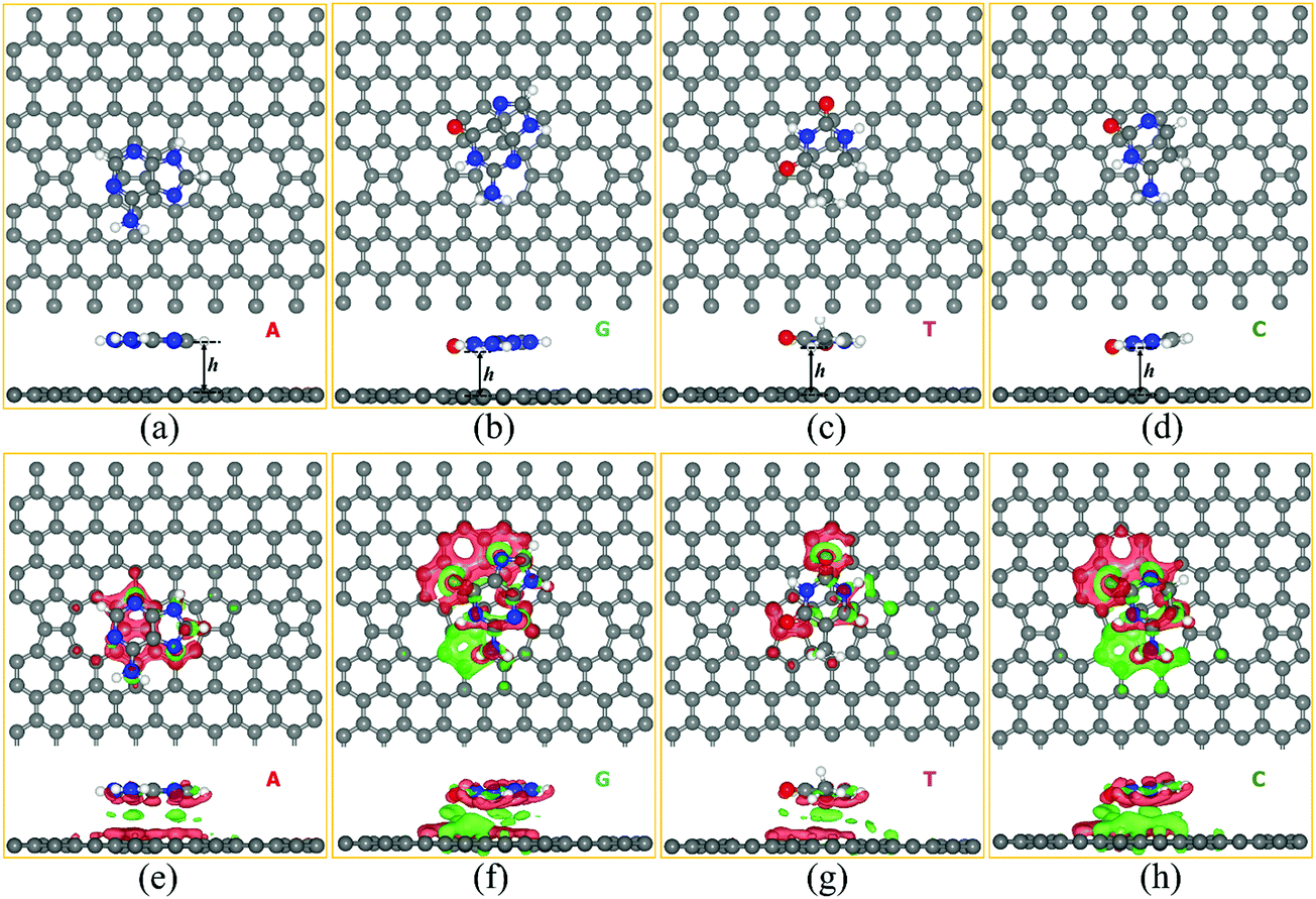 | ||
| Fig. 3 (a–d) Top and side views of the most energetically stable configurations of (a) ELDs graphene + adenine, (b) ELDs graphene + guanine, (c) ELDs graphene + thymine, and (d) ELDs graphene + cytosine systems. The adsorption heights (h, in Å) between the nucleobase molecule and the ELDs graphene sheet are shown in (a–d). Atom color code: O (red), N (blue), C (grey), and H (light white). (e–h) Charge density difference plots (top and side views, iso-surface value: 0.003 e Å−3) for ELDs graphene + nucleobase systems. The green iso-surface represents an electron loss, while the red one indicates an electron gain. | ||
The most energetically stable configurations of adsorbed A, G, T, and C on the ELDs graphene sheet were obtained using the GGA+PBE and vdW-DF-cx levels of theories. In the supporting information file, we have made a vis-à-vis comparison of the calculated results using the GGA+PBE and vdW-DF-cx level of theories. Herein, we mainly discuss the results obtained using the vdW-DF-cx level of theories. Table 1 shows the adsorption height (h) and adsorption energies between the nucleobase and the ELDs graphene sheet. The ‘h’ is the shortest vertical distance between the substrate and molecule. In the case of ELDs graphene + A, the adsorption height is the shortest distance, as shown in Fig. 3. Table 1 shows that the Eads order of all four nucleobases is G > A > C > T. It is found that the vdW-DF-cx-calculated Eads values are larger than those calculated at the GGA+PBE level of theory (Table S2, ESI†). This is because the vdW-DF-cx includes nonlocal corrections from the first-principles DFT calculations. The GGA+PBE gives relatively lower Eads values and larger adsorption heights (Table S2, ESI†), indicating that it does not correctly describe the important π–π interaction between the nucleobase and the ELDs graphene sheet. To further understand the nature of the interaction between the target DNA molecule and the ELDs graphene, we computed the total charge density difference (Δρ(r)). Practically, Δρ(r) illustrates the charge accumulation/depletion in the ELDs graphene + nucleobase system from which we can calculate the total charge transfer. Our Δρ(r) results are shown in Fig. 3(e–h) and were calculated using eqn (2) for all four nucleobase molecules on the ELDs graphene surface. A significant charge density redistribution is found for all four nucleobases with gain (red) and loss (green) of electronic charge. Based on Mulliken charge, we found that the net charges on the adsorbed nucleobases (in units of |e|) are 0.09, 0.11, 0.07, and 0.06 for A, G, T, and C, respectively. This suggests that there is a favourable interaction between the ELDs graphene surface and the target nucleobase molecule. However, Δρ(r) results do not show a strong overlap between ELDs graphene and nucleobases. Thus, looking into the Eads values, adsorption heights, and Mulliken charges of all four nucleobases on the ELDs graphene sheet, we find that the nature of the interaction is weak but enough for detection.
| Nucleobase | E ads (eV) | h (Å) |
|---|---|---|
| Adenine | −1.55 | 2.98 |
| Guanine | −1.72 | 2.71 |
| Thymine | −1.39 | 2.72 |
| Cytosine | −1.50 | 2.65 |
Further, we study the effect of nucleobase molecule adsorption on the electronic structure of the ELDs graphene using vdW-DF-cx geometries. Fig. 4 shows the calculated electronic DOS of the ELDs graphene and the ELDs graphene + nucleobase systems along with the projected DOS (PDOS) of all four nucleobases. The adsorption of nucleobase molecules leads to changes in the electronic DOS of the ELDs graphene. In the given energy window (−4 to 4 eV), we find that the nucleobase molecule introduces several strong states near the Fermi-level of the ELDs graphene. The adsorption of all four nucleobase molecules maintains the metallic nature of the ELDs graphene sheet with several strong states in the Fermi-level. Fig. 4 shows that the G nucleobase has the maximum number of electronic DOS states in the −4 to 0 eV energy window, while the T nucleobase has the least number of electronic DOS states in the given energy window. However, we find that there are a significant number of electronic DOS states available for all four nucleobase molecules, which indicates that the four nucleobase molecules couple well with the ELDs graphene sheet. Thus, to understand the action of the ELDs graphene as a DNA sequencing device, the combined NEGF+DFT method is used to study the electronic transport properties of all four nucleobases on the ELDs graphene nano-sized device.
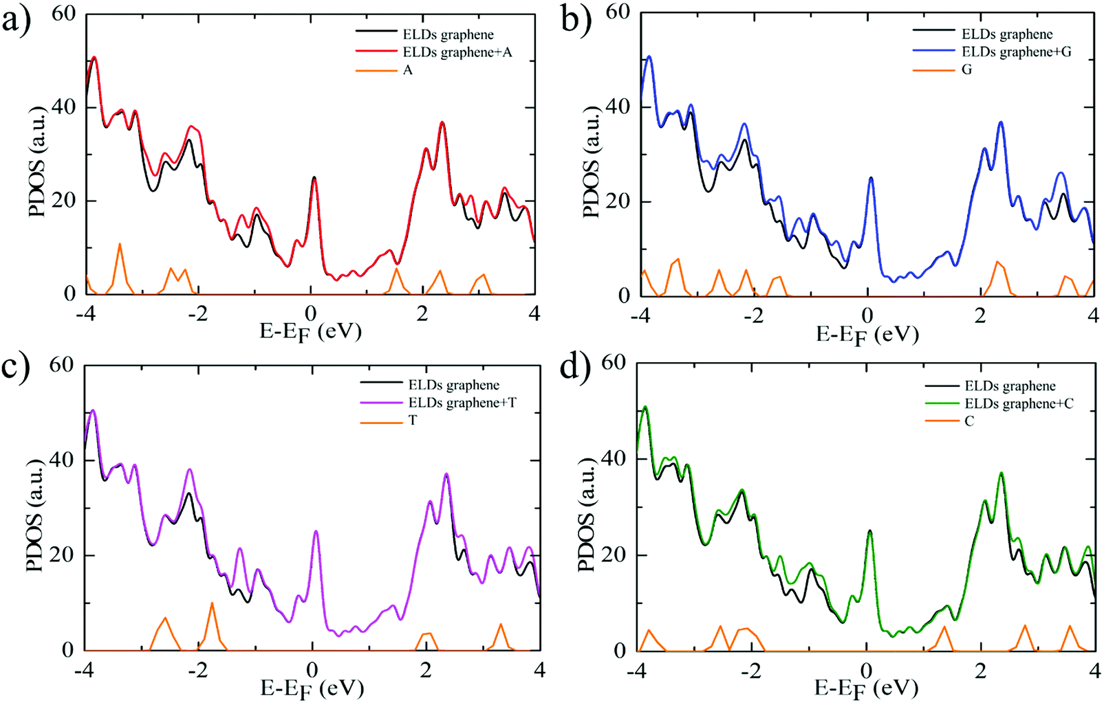 | ||
| Fig. 4 (a–d) Electronic DOS of the ELDs graphene and ELDs graphene + nucleobase systems and the PDOS for each nucleobase. The Fermi level (E − EF) is set to zero. | ||
3.3. Electronic transport properties
We investigated the T(E) of the ELDs graphene-based device for individual identification of all four nucleobases. Fig. 5a shows the zero-bias T(E) curves of the ELDs graphene and ELDs graphene + nucleobase systems as a function of energy (E). The ELDs (pristine) graphene has integer T(E) values corresponding to the number of conduction-channels. However, the ELDs graphene with a stacked nucleobase molecule presents a T(E) figure with sharp drops (dips). We understand that this could be due to the orbital overlap between the target nucleobase molecule and the ELDs graphene device, which causes dips in the T(E) of the ELDs graphene Fermi-energy level (E − EF) which can be controlled through the application of gate voltage. The T(E) curves of ELDs graphene + nucleobase systems (A/G/T/C) each show a nearly symmetric dip at different energy values, marked by coloured arrows in Fig. 5a. Interestingly, in other reports, it has been demonstrated that Fano resonance is the ruling mechanism of T(E) reduction in the molecule + graphene system.14–18,64 Therefore, the origin of the dips (sharp dips marked in Fig. 5a) appearing in the T(E) of the ELDs graphene + nucleobase molecule transport system could be due to Fano resonance. Fig. S4 (ESI†) shows the projected DOS of the ELD graphene + nucleobases. We find that px + py orbitals are interacting and the resulting π–π interactions may be the reason for the Fano resonance (Fig. 5a and b). Furthermore, we note that the size of the Fano resonance dip is affected by geometrical changes, for example, by increasing adsorption height and rotation of the DNA nucleobases with respect to the y-axis perpendicular to the ELDs graphene in the xz-plane (Fig. S5–S7; details in ESI†). This could be because of the different coupling or overlapping between the MOs of the nucleobase molecules and the ELDs graphene for a given stable-stacking configuration. The strong Fano resonance dip position varies with geometrical changes; however, it can still be used for individual identification of each nucleobase molecule on the ELDs graphene device. Herein, we discuss the most characteristic strong Fano resonance dips (i.e., those indicated by the coloured arrows in Fig. 5a). Interestingly, we found that at the energy level of the most characteristics sharp dips, strongly mixed MOs between the ELDs graphene and base molecules are found whose base part well corresponds to the frontier molecular orbitals, as shown in Fig. 5c–f. For example, if we look at the T(E) curve of the ELDs graphene + G, we find that the dip for G (at E − EF = −0.52 eV) shows strong resonance between G MOs and the ELDs graphene + G MOs which partially blocks the ballistic conductance-channels of the ELDs graphene device, as shown in Fig. 5a and c. The mixed orbital at the dip position has a strong resemblance to the G HOMO (highest occupied molecular orbital). Similarly, if we look at the transmission spectra of ELDs graphene + A and ELDs graphene + C, we find that the dip positions are at E − EF = −0.78 eV (Fig. 5a). Both the nucleobases (A and C) show that the highly mixed orbitals at the dip position are the HOMOs, as shown in Fig. 5d and e. In the case of ELDs graphene + T, the HOMO is nearly degenerate to the HOMO−1, with an energy difference of about 0.08 eV (Fig. 5a). Fig. 5a shows two dips around −1.21 eV. Both the dips are near matches with the energy difference between the HOMO and the HOMO−1. Fig. 5f shows only MOs corresponding to the right dip at E − EF = −1.21 eV; however, those corresponding to the left dips were also found. Thus, we have seen in all four systems that each strong resonance dip in the T(E) curve has a corresponding MO of the base molecules, which may be playing the role of a resonator.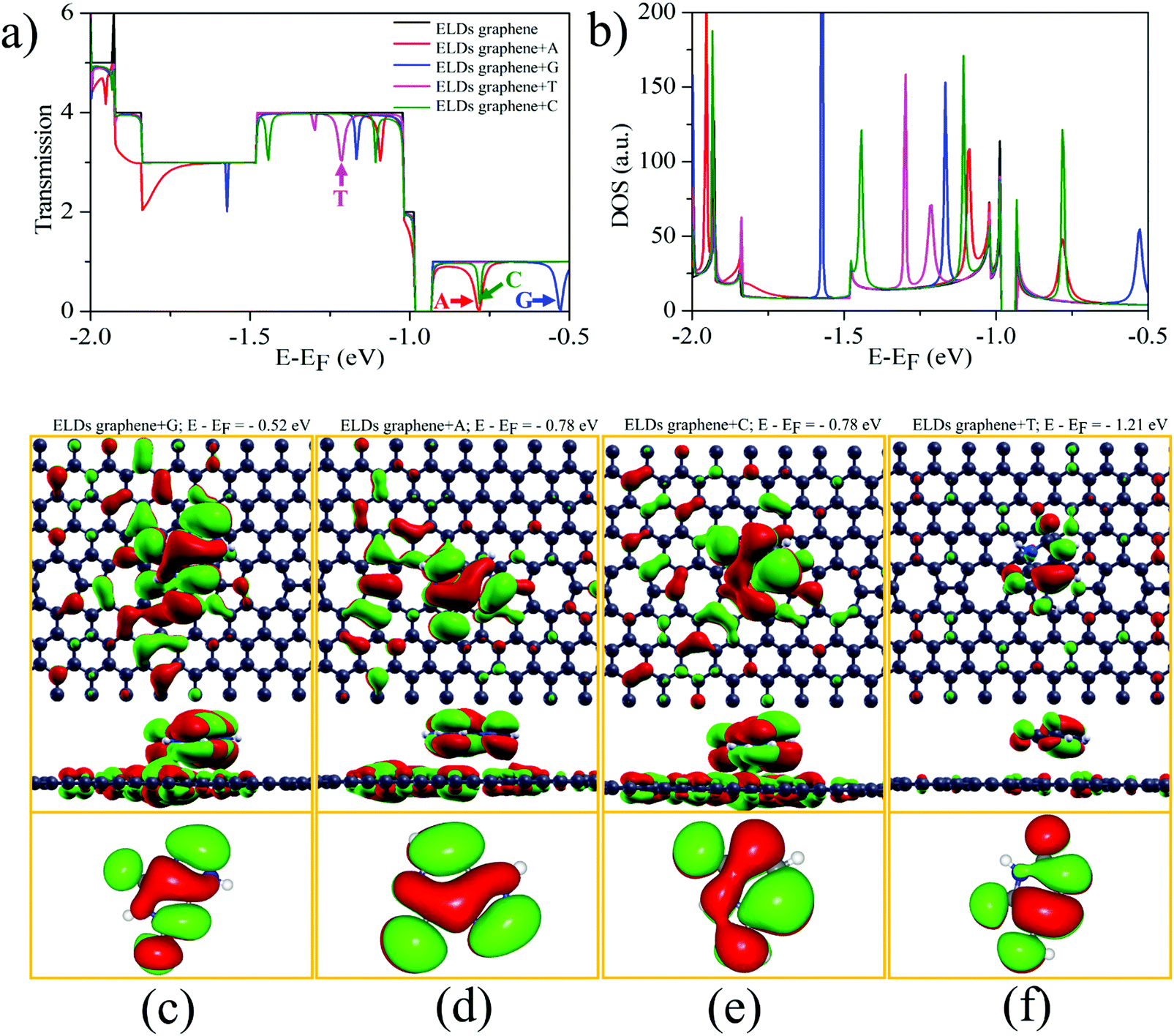 | ||
| Fig. 5 (a) The zero-bias transmission functions of the ELDs graphene and ELDs graphene + nucleobase systems showing the characteristics dips of each nucleobase. (b) Electronic density of states. (c–f) MOs for the ELDs graphene + nucleobase systems responsible for transmission dips. | ||
Further, to verify that the strong dips result from the Fano resonance, we studied the T(E) and DOS of the ELDs graphene + nucleobase systems at increasing adsorption heights, as shown in Fig. S6 (details in ESI†). As the distance between target nucleobase molecules and the ELDs graphene increases, the resulting coupling reduces the dip width of the T(E), although the coupling strength does not change considerably for adsorbed nucleobases at a stacking height (h = 3.5 Å) due to the strong π–π interaction. Therefore, it is noted that the position of Fano resonance dips is sensitive to the interaction strength. Additionally, all four nucleobases were rotated around the y-axis from 0° to 180° in steps of 30° (Fig. S7, details in ESI†). We observed some changes in the dip position and width of the T(E), though not significant, which could be due to a similar environment. Hence, the ultra-sensitive ELDs graphene-based device can be utilized for DNA sequencing.
Next, from the experimental point of view, we investigated the conductance sensitivity of the ELDs graphene device with all four nucleobases. In general, sensitivity is dependent on the conductance changes of the device induced by the DNA molecule adsorption. The conductance sensitivity (S%) can be defined as S(%) = |G0 − G/G0|, where G0 and G are the transmissions of the ELDs graphene and the ELDs graphene + nucleobase system, respectively. The conductance sensitivity (at ∼0.04 eV, Fig. S8, ESI†) plot for all four nucleobases is shown in Fig. 6a, measured during experimental realization using a gate voltage of ∼0.04 V. We noted the S% values are about 29%, 76%, 59%, and 52% for A, G, T, and C, respectively. The maximum S% values follow the sequence G > T > C > A. Such high S% values are significant for the individual identification of all four DNA nucleobases. Note that the results in Fig. 6a are given as a function of the relevant Eads in eV. Consequently, it is not the influence of the strength of the interaction, but rather the different type of DNA nucleobase molecules that controls the conductance sensitivity. Kim et al. revealed that the orbital interaction (coupling) order can match the Eads values.16 However, in our study, we have four different types of DNA nucleobase molecules and the coupling need not be in the same order as their Eads values. Thus, our results indicate that the ELDs graphene-based device possesses highly sensitive conductance resolution for the electrical detection of each nucleobase at a specific gate voltage.
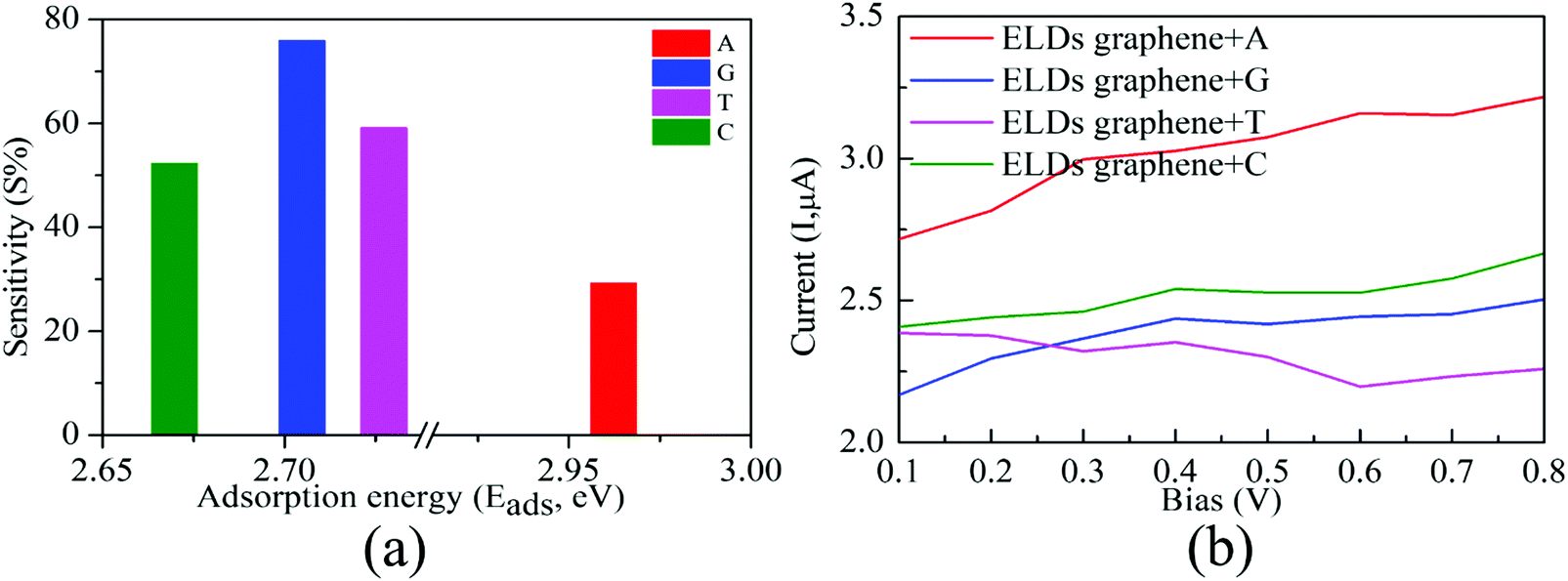 | ||
| Fig. 6 (a) The conductance sensitivity vs. adsorption energy plot at a specific energy of −0.042 eV for all four ELDs graphene + nucleobase systems. (b) I–V characteristics of all four ELDs graphene + nucleobase systems. | ||
Further, we note that the conduction reductions for C and A overlap (Fig. 5a). However, the overall transmission function is different for each nucleobase (C and A). This is because they are two different types of nucleobases: (i) purine (A and G) and (ii) pyrimidine (C and T). The pyrimidine-based nucleobases are smaller in size than the purine-based nucleobases and the number of hydrogens available for interactions are also different in these two cases. This is one of the reasons for the different coupling of C and A nucleobases with ELDs graphene electrodes. Consequently, the overall transmission function is different for nucleobases C and A. Furthermore, we note that conductance sensitivity (S%) values are about 29% and 52% for A and C (Fig. 6a), respectively. The maximum S% values also follow the order C > A. Such high S% values are significant for the individual identification of these two nucleobases. Moreover, the calculated unique electric current (I) signal can also be utilized to detect these two nucleobases (Fig. 6b). Hence, we find that it is possible to distinguish between these two nucleobases on the ELDs graphene nanosensor.
3.4. Current–voltage (I–V) characteristics
We computed the I–V characteristics for the detection of all four nucleobases on the ELDs graphene device. Fig. 6b depicts the I–V curve for the ELDs graphene + nucleobase systems. We found that probing the A nucleobase results in an electric current (I) which is significantly higher than those for the other three nucleobases in the given bias window (0.1–0.8 V). The current signal for the T nucleobase is smaller than that of the A nucleobase and, at 0.8 V bias, there is a considerable difference between these two nucleobases. In the case of G and C, although they mostly run parallel to each other, still one can see that there is a constant difference between these two nucleobases. Hence, it may be possible to distinguish between G and C nucleobases in the given bias window (0.1–0.8 V). The I–V curve of the ELDs graphene + G system gradually increases. However, in the ELDs graphene + T system, we find a reduction of the I–V curve compared to the other three nucleobases (A, G, and C) in the same bias window. This may be because of the negative differential resistance (NDR) and coupling strength.29 The orbital interaction (coupling between ELDs graphene + nucleobase) is not necessarily in the same order for all the nucleobases in the same bias window. Furthermore, it is noted that we have four different types of DNA nucleobases and the orbital interactions (coupling strength between ELDs graphene + nucleobase) are not necessarily in the same order as their Eads values.16 Thus, change in current signals with respect to applied bias voltage depends on the coupling between electrode + nucleobase orbitals. Once the system is in the non-equilibrium state, the movement of the HOMO/LUMO peaks associated with the nucleobase molecules plays a very important role in current signals with changes in applied bias voltage.19,28–33 We, therefore, put forward that the voltage window of 0.3–0.8 V may be required for individual identification of all four nucleobases on the ELDs graphene device. More precisely, A and T nucleobases can be identified based on the higher and lower current values, respectively, while G and C can be identified between the other two nucleobases. Therefore, the I–V curves reflect that varying bias voltage may allow all four nucleobases to be identified. Thus, based on our results, it may be possible to distinguish the four nucleobases using the ELDs graphene device.4. Conclusions
In conclusion, we demonstrated that using one-dimensional extended topological line defects in graphene may be useful for DNA sequencing applications. Using the DFT approach, we studied the interaction strengths between ELDs graphene and all four DNA nucleobases. DNA nucleobases are likely to be physisorbed on the ELDs graphene device in stable stacking-like configurations, with adsorption energy values in the following sequence: G > A > C > T. Furthermore, using DFT+NEGF formalism, we have shown that the individual identification of all four DNA nucleobases is, in principle, possible through electronic transmission function, conductance sensitivity (S%), and I–V characteristics measurements. We show that the π–π interaction is responsible for the interaction between the nucleobase molecule and the ELDs graphene surface; the resulting coupling gives a strong Fano resonance in the transmission functions of ELDs + nucleobases. The computed molecular orbitals at specific energy values show that there is strong orbital overlapping between the ELD graphene and nucleobase molecules. Such features of the nucleobase molecules occur due to characteristic molecular orbital coupling dips. Moreover, we demonstrated that the sensing performance can be improved by applying a specific gate voltage. The calculated maximum conductance sensitivities are in the sequence G > T > C > A. These high conductance sensitivity values are significant for the individual identification of all four nucleobases. Also, the calculated I–V characteristics results indicate that a voltage window of 0.3–0.8 V may be required for the individual identification of all four nucleobases on the ELDs graphene device. Thus, we predict that developing such a nano-sized device could be very promising for individual identification of DNA nucleobases.Conflicts of interest
There are no conflicts of interest to declare.Acknowledgements
We acknowledge IIT Indore for the lab and computing facilities. This work is supported by DST-SERB (Project Number: CRG/2018/001131), CSIR [Grant Number: 01(2886)/17/EMR (II)], and SPARC/2018-2019/P116/SL. R. L. K. acknowledges MHRD for senior research fellowship (SRF).References
- Z. S. Siwy and M. Davenport, Nat. Nanotechnol., 2010, 5, 697–698 CrossRef CAS.
- E. C. Hayden, Nature, 2014, 507, 294–295 CrossRef.
- H. Arjmandi-Tash, L. A. Belyaeva and G. F. Schneider, Chem. Soc. Rev., 2016, 45, 476–493 RSC.
- S. J. Heerema and C. Dekker, Nat. Nanotechnol., 2016, 11, 127–136 CrossRef CAS.
- H. Liu, J. He, J. Tang, H. Liu, P. Pang, D. Cao, P. Krstic, S. Joseph, S. Lindsay and C. Nuckolls, Science, 2010, 327, 64–67 CrossRef CAS.
- D. Branton, D. W. Deamer, A. Marziali, H. Bayley, S. A. Benner, T. Butler, M. D. Ventra, S. Garaj, A. Hibbs, X. Huang, S. B. Jovanovich, P. S. Krstic, S. Lindsay, X. S. Ling, C. H. Mastrangelo, A. Meller, J. S. Oliver, Y. V. Pershin, J. M. Ramsey, R. Riehn, G. V. Soni, V. Tabard-Cossa, M. Wanunu, M. Wiggin and J. A. Schloss, Nat. Biotechnol., 2008, 26, 1146–1153 CrossRef CAS.
- B. Pathak, H. Löfås, J. Prasongkit, A. Grigoriev, R. Ahuja and R. H. Scheicher, Appl. Phys. Lett., 2012, 100, 023701 CrossRef.
- T. Nelson, B. Zhang and O. V. Prezhdo, Nano Lett., 2010, 10, 3237–3242 CrossRef CAS.
- J. He, L. Lin, P. Zhang and S. Lindsay, Nano Lett., 2007, 7, 3854–3858 CrossRef CAS.
- J. He, L. Lin, H. Liu, P. Zhang, M. Lee, O. F. Sankey and S. M. Lindsay, Nanotechnology, 2009, 20, 075102 CrossRef.
- S. Huang, J. He, S. Chang, P. Zhang, F. Liang, S. Li, M. Tuchband, A. Fuhrmann, R. Ros and S. Lindsay, Nat. Nanotechnol., 2010, 5, 868–873 CrossRef CAS.
- S. Chang, S. Huang, J. He, F. Liang, P. Zhang, S. Li, X. Chen, O. Sankey and S. Lindsay, Nano Lett., 2010, 10, 1070–1075 CrossRef CAS.
- S. Biswas, S. Sen, J.-O. Im, S. Biswas, P. Krstic, B. Ashcroft, C. Borges, Y. Zhao, S. Lindsay and P. Zhang, ACS Nano, 2016, 10, 11304–11316 CrossRef CAS.
- S. K. Min, W. Y. Kim, Y. Cho and K. S. Kim, Nat. Nanotechnol., 2011, 6, 162–165 CrossRef CAS.
- Y. Cho, S. K. Min, W. Y. Kim and K. S. Kim, Phys. Chem. Chem. Phys., 2011, 32, 14293–14296 RSC.
- M. R. Rezapour, A. C. Rajan and K. S. Kim, J. Comput. Chem., 2014, 35, 1916–1920 CrossRef CAS.
- A. C. Rajan, M. R. Rezapour, J. Yun, Y. Cho, W. J. Cho, S. K. Min, G. Lee and K. S. Kim, ACS Nano, 2014, 8, 1827–1833 CrossRef CAS.
- S. Thomas, A. C. Rajan, M. R. Rezapour and K. S. Kim, J. Phys. Chem. C, 2014, 118, 10855–10858 CrossRef CAS.
- R. L. Kumawat and B. Pathak, J. Phys. Chem. C, 2019, 123, 22377–22383 CrossRef CAS.
- F. Traversi, C. Raillon, S. M. Benameur, K. Liu, S. Khlybov, M. Tosun, D. Krasnozhon, A. Kis and A. Radenovic, Nat. Nanotechnol., 2013, 8, 939–945 CrossRef CAS.
- C. A. Merchant, K. Healy, M. Wanunu, V. Ray, N. Peterman, J. Bartel, M. D. Fischbein, K. Venta, Z. Luo, A. T. C. Johnson and M. Drndic, Nano Lett., 2010, 10, 2915–2921 CrossRef CAS.
- S. Garaj, W. Hubbard, A. Reina, J. Kong, D. Branton and J. A. Golovchenko, Nature, 2010, 467, 190–193 CrossRef CAS.
- K. Liu, J. Feng, A. Kis and A. Radenovic, ACS Nano, 2014, 8, 2504–2511 CrossRef CAS.
- A. B. Farimani, K. Min and N. R. Aluru, ACS Nano, 2014, 8, 7914–7922 CrossRef CAS.
- K. K. Saha, M. Drndić and B. K. Nikolić, Nano Lett., 2012, 12, 50–55 CrossRef CAS.
- L. J. Steinbock and A. Radenovic, Nanotechnology, 2015, 26, 074003 CrossRef CAS.
- H. W. C. Postma, Nano Lett., 2010, 10, 420–425 CrossRef CAS.
- J. Prasongkit, A. Grigoriev, B. Pathak, R. Ahuja and R. H. Scheicher, Nano Lett., 2011, 11, 1941–1945 CrossRef CAS.
- J. Prasongkit, A. Grigoriev, B. Pathak, R. Ahuja and R. H. Scheicher, J. Phys. Chem. C, 2013, 117, 15421–15428 CrossRef CAS.
- H. He, R. H. Scheicher, R. Pandey, A. R. Rocha, S. Sanvito, A. Grigoriev, R. Ahuja and S. P. Karna, J. Phys. Chem. C, 2008, 112, 3456–3459 CrossRef CAS.
- V. Shukla, N. K. Jena, A. Grigoriev and R. Ahuja, ACS Appl. Mater. Interfaces, 2017, 9, 39945–39952 CrossRef CAS.
- R. L. Kumawat, P. Garg, S. Kumar and B. Pathak, ACS Appl. Mater. Interfaces, 2019, 11, 219–225 CrossRef CAS.
- R. L. Kumawat, P. Garg, G. Bhattacharyya and B. Pathak, ACS Appl. Electron. Mater., 2020, 2, 1218–1225 CrossRef CAS.
- J. Shendure and H. Ji, Nat. Biotechnol., 2008, 26, 1135–1145 CrossRef CAS.
- M. Liu, H. Zhao, S. Chen, H. Yu and X. Quan, Chem. Commun., 2012, 48, 564–566 RSC.
- T. Ahmed, S. Kilina, T. Das, J. T. Haraldsen, J. J. Rehr and A. V. Balatsky, Nano Lett., 2012, 12, 927–931 CrossRef CAS.
- S. Akca, A. Foroughi, D. Frochtzwajg and H. W. C. Postma, PLoS One, 2011, 6, 4–7 CrossRef.
- S. Gowtham, R. H. Scheicher, R. Ahuja, R. Pandey and S. P. Karna, Phys. Rev. B: Condens. Matter Mater. Phys., 2007, 76, 033401 CrossRef.
- J. Antony and S. Grimme, Phys. Chem. Chem. Phys., 2008, 10, 2722–2729 RSC.
- D. Le, A. Kara, E. Schroder, P. Hyldgaard and T. S. Rohman, J. Phys.: Condens. Matter, 2012, 24, 424210 CrossRef.
- B. Song, G. Cuniberti, S. Sanvito and H. Fang, Appl. Phys. Lett., 2012, 100, 063101 CrossRef.
- F. Ortmann, W. G. Schmidt and F. Bechstedt, Phys. Rev. Lett., 2005, 95, 186101 CrossRef CAS.
- K. Berland, S. D. Chakarova-Käck, V. R. Cooper, D. C. Langreth and E. Schröder, J. Phys. Condens. Matter, 2011, 23, 135001 CrossRef.
- R. G. Amorim and R. H. Scheicher, Nanotechnology, 2015, 26, 154002 CrossRef.
- Q. Lin, X. Zou, G. Zhou, R. Liu, J. Wu, J. Li and W. Duan, Phys. Chem. Chem. Phys., 2011, 13, 12225–12230 RSC.
- H. S. Kim and Y. H. Kim, Biosens. Bioelectron., 2015, 69, 186–198 CrossRef CAS.
- N. Yang and X. Jiang, Carbon, 2017, 115, 293–311 CrossRef CAS.
- M. Drndic, Nat. Nanotechnol., 2014, 9, 743 CrossRef CAS.
- K. S. Novoselov, A. K. Geim, S. V. Morozov, D. Jiang, Y. Zhang, S. V. Dubonos, I. V. Grigorieva and A. A. Firsov, Science, 2004, 306, 666–669 CrossRef CAS.
- A. K. Geim and K. S. Novoselov, Nat. Mater., 2007, 6, 183–191 CrossRef CAS.
- J. Lahiri, Y. Lin, P. Bozkurt, I. I. Oleynik and M. Batzill, Nat. Nanotechnol., 2010, 5, 326–329 CrossRef CAS.
- J.-H. Chen, G. Autes, N. Alem, F. Gargiulo, A. Gautam, M. Linck, C. Kisielowski, O. Yazyev, S. Louie and A. Zettl, Phys. Rev. B: Condens. Matter Mater. Phys., 2014, 89, 121407 CrossRef.
- D. Kim, Y. Kim, J. Ihm, E. Yoon and G.-D. Lee, Carbon, 2015, 84, 146–150 CrossRef CAS.
- F. A. L. de Souza, R. G. Amorim, J. Prasongkit, W. L. Scopel, R. H. Scheicher and A. R. Rocha, Carbon, 2018, 129, 803–808 CrossRef CAS.
- J. Prasongkit, E. D. F. Martins, F. A. L. de Souza, W. L. Scopel, R. G. Amorim, V. Amornkitbamrung, A. R. Rocha and R. H. Scheicher, J. Phys. Chem. C, 2018, 122, 7094–7099 CrossRef CAS.
- M. J. Frisch, G. W. Trucks, H. B. Schlegel, G. E. Scuseria, M. A. Robb, J. R. Cheeseman, G. Scalmani, V. Barone, B. Mennucci, G. A. Petersson and H. Nakatsuji, Gaussian 09, Revision A.1., Gaussian, Inc., Wallingford CT, 2009 Search PubMed.
- P. Ordejón, E. Artacho and J. M. Soler, Phys. Rev. B: Condens. Matter Mater. Phys., 1996, 53, 10441–10444 CrossRef.
- M. Brandbyge, J. L. Mozos, P. Ordejón, J. Taylor and K. Stokbro, Phys. Rev. B: Condens. Matter Mater. Phys., 2002, 65, 165401 CrossRef.
- C. Lee, W. Yang and R. G. Parr, Phys. Rev. B: Condens. Matter Mater. Phys., 1988, 37, 785–789 CrossRef CAS.
- K. Berland and P. Hyldgaard, Phys. Rev. B: Condens. Matter Mater. Phys., 2014, 89, 035412 CrossRef.
- N. Troullier and J. L. Martins, Phys. Rev. B: Condens. Matter Mater. Phys., 1991, 43, 1993–2006 CrossRef CAS.
- S. Dutta, Electronic transport in mesoscopic systems, Cambridge University Press, Cambridge, 1995 Search PubMed.
- R. L. Kumawat and B. Pathak, Nanoscale Adv., 2020, 2, 4041–4050 RSC.
- R. L. Kumawat and B. Pathak, Appl. Surf. Sci., 2020, 529, 147094 CrossRef CAS.
Footnote |
| † Electronic supplementary information (ESI) available: Details regarding the adsorption sites, initial and final adsorption configurations, relative energies, comparative discussion of GGA-PBE and vdW-DF-cx results, projected DOS, mechanism of increasing adsorption heights and structural rotation, transmission function and density of states of the ELDs graphene + nucleobase systems due to change in adsorption heights and rotation of the nucleobase, transmission function and electronic density of states at zero-bias are given. See DOI: 10.1039/d0ma00617c |
| This journal is © The Royal Society of Chemistry 2020 |