
 Open Access Article
 This Open Access Article is licensed under a Creative Commons Attribution-Non Commercial 3.0 Unported Licence
Characterization of SERS platforms designed by electrophoretic deposition on CVD graphene and ITO/glass†
Federico
Fioravanti
 a,
David
Muñetón Arboleda
b,
Gabriela I.
Lacconi
*a and
Francisco J.
Ibañez
*b
a,
David
Muñetón Arboleda
b,
Gabriela I.
Lacconi
*a and
Francisco J.
Ibañez
*b
aInstituto de Investigaciones en Físico-Química de Córdoba (INFIQC), CONICET, Dpto. de Fisicoquímica, Facultad de Ciencias Químicas, Universidad Nacional de Córdoba, Haya de La Torre-Medina Allende, 5000 Córdoba, Argentina. E-mail: glacconi@fcq.unc.edu.ar
bInstituto de Investigaciones Fisicoquímicas, Teóricas y Aplicadas (INIFTA), Universidad Nacional de La Plata – CONICET, Sucursal 4 Casilla de Correo 16 (1900), La Plata, Argentina. E-mail: fjiban@inifta.unlp.edu.ar
First published on 23rd June 2020
Abstract
Here, we perform electrophoretic deposition (EPD) to control the assembly of citrate-coated Au nanoparticles (NPs) on ITO/glass and graphene. Monolayer graphene is obtained by CVD and transferred to ITO/glass free of polymer. A quick surface-enhanced Raman scattering (SERS) test determined that the optimal platform consists of drop-casting methylene blue (MB) onto as-deposited Au NPs (600 s at 1.0 V) to achieve 150× signal enhancement. Therefore, we proceeded in the same manner and deposited Au NPs under identical EPD conditions on graphene/ITO/glass. Then, we tested both platforms by immersing into 0.3 mM MB solution and found similar SERS intensity on the graphene- and ITO-containing platforms after 10 min and 66 h, respectively, which clearly demonstrates the importance of the substrate. To characterize the platforms, linear scan voltammetry (LSV) and SEM were used for assigning the NPs’ oxidation peaks to their corresponding areas on the image. We found good agreement with respect to the number of NPs per μm2 as measured by LSV and SEM. We observed that EPD on graphene leads to six-fold larger coverage than on ITO/glass. These Au NPs were mostly assembled in the form of agglomerates located on the defects of graphene. If those agglomerates are dissolved by anodic stripping, no SERS signal was found from the MB analyte. This also demonstrates that the platform can be reused for further deposition and SERS analysis. This work provides a simple and controllable method for the design of advanced SERS platforms.
Introduction
The combination of metal nanoparticles (NPs) and graphene has many benefits for applications in the areas of sensing,1,2 photocatalysis,3 photovoltaics,4 light harvesting devices,7 electronics,5 and detection via surface-enhanced Raman scattering (SERS).2,6,8 This is possible due to the strong synergy between both nanomaterials. For example, in light harvesting studies, the presence of metallic NPs expands the spectrum to visible, while graphene reinforces the electronic transport across the platform.7 In electronics, selective Au NPs deposition is useful for healing defect areas on graphene.5 Detection via molecular sensing and SERS of dye molecules adsorbed on graphene–NPs is possible due to the different stacking configurations of graphene grown on 3D Ni foam.8 In SERS applications, it has been demonstrated that while the presence of Au or Ag NPs allows a critical signal enhancement, graphene plays a role by quenching the fluorescence and luminescence of the analyte molecules and metallic NPs, respectively.2 Previous examples clearly demonstrate that the combination of these two nanomaterials brings about high expectations in identifying some phenomena and discovering new synergies between them. Nowadays, new technologies are emerging, for example, flexible platforms for point-of-care diagnostics employing SERS as a highly sensitive and non-invasive approach.9 Perhaps one of the main challenges is to control the deposition of metallic NPs on flexible graphene in order to form heterostructures with enhanced properties. This is a major issue because depending on how plasmonic NPs (active SERS entities) arrange on the vast surface of graphene, some of the aforementioned attributes can be further improved.Electrophoretic deposition (EPD) has become the method of choice due to its versatility and control of the nanomaterial to be deposited. It has been demonstrated to override other deposition methods because it is scalable,10 film thickness can be easily controlled11 and formed within seconds.12 It has gained much attention recently due to the work of Zamborini and co-workers who introduced mediator molecules such as hydrogen peroxide16 and hydroquinone (HQ)17 which served to neutralize the negatively-charged nanospheres (NSs), and therefore induced deposition onto the electrode due to charge destabilization. This permitted fine control of the deposition of metal NSs of various sizes on ITO/glass electrodes. The size-dependent properties were monitored by linear scan voltammetry (LSV) that exhibited oxidation peaks at different potentials for Ag13,14 and Au15–18 NSs during anodic stripping.19 This comes from the seminal work of Ivanova et al.,13 who experimentally corroborated what Plieth thermodynamically calculated20 regarding the dependence of cluster size on the oxidation potential. Besides the size of NSs, shifts in peak potential have been demonstrated for the same NPs placed on different types of substrates,21 different NP compositions in core–shell configurations,22 NP agglomeration,23 functionalized electrodes,14 and different deposition methods.24 For example, Brainina et al. found that the oxidation peak potential appeared more positive when 20 nm diam. Au NPs were placed onto Pt or Au electrodes with respect to the same NPs on glassy carbon (GC). They calculated the Gibbs free energy of the as-deposited NPs on these substrates and demonstrated good agreement with the experimental LSV peaks. In line with this, Masitas et al., electrostatically placed 9 nm diam. Ag NSs on different substrates including ITO–glass and GC-, Pt-, and Au-microelectrodes.14 They determined that the oxidation potentials of Au NSs on the Au and Pt microelectrodes also shifted more positive than on GC. Later, Pattadar et al., from the same group, compared different deposition methods including EPD, drop casting, and electrostatic attachment of Au NSs and determined that the oxidation potentials for EPD appeared more positive with respect to those NSs electrostatically attached.25 Allen et al. synthesized citrate-coated 4, 15, and 50 nm diam. Au NSs and varied the pH from 9 to 1.8 in order to follow the different stages of agglomeration by using UV-vis spectroscopy and LSV. They determined that as long as the pH decreases, the 4 and 15 nm diam. NSs shifted to more positive potentials, whereas the 50 nm NSs were unsusceptible to pH changes.23 These findings are quite relevant for EPD and could be further employed in SERS applications due to the fine control over NP sizes, film thickness, and NP distribution and arrangements on the surface for just mentioning a few.
Surprisingly, EPD on graphene has been scarcely explored.26,27 For instance, Semaltianos et al. obtained Au NPs by laser ablation and performed EPD at 30 V for 20 and 60 min and found relatively well-distributed NPs on graphene. However, at such high potentials and extended times, graphene was oxidized.26 Most of the studies related to the deposition of nanoclusters on graphitic structures (i.e., HOPG) started with Penner’ s group who selectively deposited metal and metal–oxide nanoclusters via electrochemical methods.28–30 Selective deposition sites were previously studied by McCreery and co-workers who demonstrated higher electron transfer on the generated defects on graphite (i.e., step-edges) caused by laser or electrochemical pre-treatments.31 For instance, anodization of HOPG led to the formation of oxygen-containing groups preferentially at step edges.32–34 Interestingly, other groups have shown electroless deposition of metal NPs on HOPG33,34 and on graphene.4,34,35 For instance, Lomax and Dryfe performed in situ AFM and electrochemistry in an open cell and observed in situ growth of Au NPs on HOPG.34 Kong and co-workers demonstrated that less than 20 s of exposure of CVD graphene to HAuCl4 solution caused spontaneous nucleation and growth of Au NPs preferentially formed on the wrinkles of graphene.4,36 This particular phenomenon has found practical uses such as healing graphene at defect areas for further improving the conductivity in the presence of metallic NPs.5 Dalfovo et al. demonstrated other forms of spontaneous deposition of metal NPs on graphene via van der Waals interactions between the organic alkane chains surrounding the Au core and the hydrophobic surface of graphene.2 This strong interaction was used later for forming heterostructures (graphene–NPs) and transferring graphene to a desired substrate for different applications.6 Since the EPD process requires positive potentials (1.0 V) to attract the negatively-charged Au NPs, it is reasonable to expect that oxygen-functional groups already formed on the graphene surface. Those specific areas can be wrinkles, grain boundaries, and step edges on graphene that may act as active sites for deposition of negatively-charged citrate-coated Au NPs. In this context, Ananthoju et al. systematically engineered structural defects on basal planes of CVD graphene in order to preferentially electrodeposit Au NPs for improving SERS.37 They were able to detect concentrations as low as 10−16 M Rhodamine 6G, which is 108 orders of magnitude higher than the Raman signal of the analyte.
Our goal in this work is to characterize the already constructed SERS platforms obtained by EPD of Au NPs on ITO/glass and graphene/ITO/glass followed by drop-casting or immersion of the platforms in 0.3 mM MB. For both platforms, we encountered agglomerated Au NPs likely induced by ethanol-containing MB dye; however, those NPs on graphene appeared much more agglomerated. OES, SEM and LSV techniques were crucial for determining the NP size in solution and later assigning each corresponding area to a specific oxidation potential. Characterization of the SERS platforms is very important because, for example, the literature has shown that the EPD of Au NSs on ITO (without MB) produced well-distributed NPs along the entire surface17 with no agglomerates whatsoever, whereas herein, there are some agglomerated NPs as determined by SEM and LSV peaks. The Au NPs on graphene are way more aggregated than on ITO, which is likely due to the effect of the substrate since the EPD geometrical area was kept constant for ITO and graphene. Surprisingly, those agglomerated Au NPs on graphene oxidized at lower potentials compared to the same NPs on ITO/glass. A quick SERS test by drop casting MB on EPD samples revealed that 600 s deposition is enough for achieving 1.5 orders of magnitude greater Raman signal. On the other hand, immersion of both platforms (600 s EPD) in 0.3 MB dye demonstrated that for achieving similar SERS, the graphene-containing platform required just 10 min immersion, while ITO/glass needed 66 h. In this work, we explore and characterize optimal platforms for SERS applications. The construction of these platforms is achieved by using well-controlled techniques such as EPD along with exhaustive characterization carried out using SEM and LSV.
Experimental section
Chemicals
Sodium borohydride (99%) and hydroquinone (99%), trisodium citrate salt, potassium perchlorate, nitric acid, ammonium persulfate, methylene blue and potassium bromide were purchased from Sigma Aldrich Chemicals. HAuCl4·3H2O was prepared from a high purity Au coin. Milli-Q grade water was used for all the solutions.Chemical synthesis of citrate-stabilized Au NPs
An aqueous Au NP dispersion was synthesized following the seed method reported by Murphy.38 Briefly, 0.5 mL of a 0.01 M solution of the metal salt and 0.5 mL of 0.01 M trisodium citrate were added to 18.5 mL of nanopure water. Then, 0.6 mL of ice-cold 0.1 M NaBH4 was added to the solution and stirred moderately for 2 h. The color of the solution changed to orange immediately after the addition of NaBH4 and then turned reddish indicating the formation of Au NPs.CVD graphene and transfer
Graphene (G) was grown by chemical vapor deposition (CVD) on 25 μm thick Cu foil (MTI Corp.) following the same procedure as reported recently.39 The transfer protocol follows the biphasic transferring method reported by Zhang et al. with some modifications.40 Briefly, once graphene is etched away from the bottom side of Cu with 4.0 M HNO3, the Cu piece (1 × 1 cm) with just graphene on top is brought into the biphasic solution consisting of 0.1 M ammonium persulfate and hexane. The bottom aqueous solution is extracted gently several times and refilled with nanopure water to a complete volume. When all Cu is completely dissolved, the graphene film is transferred to a clean ITO/glass electrode.UV-vis spectra and OES calculations
UV-vis spectroscopy of the as-synthesized Au NP dispersions was performed on a UV-vis PerkinElmer Lambda 35 spectrophotometer in a wavelength range between 300 and 900 nm. Optical extinction spectroscopy (OES) was used to determine the size distribution of the Au NPs in the suspensions obtained from the fit of the experimental extinction spectra and calculated by Mie–Gans theory with size corrections.41EPD conditions
Electrochemical experiments were carried out using an Autolab (PGSTAT30 ECOCHEMIE) and 600 E (CH Instruments Inc.) potentiostat for EPD and LSV experiments with a 3-electrode setup with ITO/glass (Rs = 8–12 Ω, purchased from Delta Technologies Ltd) as the working electrode, platinum foil as the counter electrode, and a saturated calomel electrode (SCE) as the reference electrode (0.243 V vs. RHE). The three electrodes faced each other, with a distance of approximately 1.0 cm between them, and with the conductive side of the ITO/glass facing the reference and counter electrodes. The EPD experiments were performed using the same parameters, as follows: the same geometric area (0.75 cm2) of the working electrodes (ITO/glass and transferred G on ITO/glass) was immersed in a solution containing 13.4 mL of nanopure water, 3.3 mL of NP solution and 3.3 mL of 0.1 M HQ added a few seconds before the experiment. Finally, 1.0 V was applied to the ITO/glass working electrode at different times including 120, 600, and 1800 s. Transients (current vs. time) at each time were recorded.Characterization of SERS platforms
Results and discussion
Characterization of EPD of Au nanoparticles on ITO/glass
Fig. 1A shows the UV-vis spectrum of the as-synthesized citrate-coated Au NPs along with a red dashed curve that represents the theoretical fit obtained by optical extinction spectroscopy (OES). Fig. 1B shows the linear scan voltammetry (LSV) curve of the as-deposited Au NPs that were dissolved after anodic stripping in 10 mM KBr plus 0.1 M KClO4 solution at a scan rate of 0.01 V s−1. The Au NPs were deposited by the electrophoretic deposition (EPD) method run for 600 s (further details are in the Experimental section). The UV-vis spectrum taken from the Au NP dispersion shows a single plasmon band centered around 515 nm, whereas the anodic stripping of the as-deposited Au NPs exhibits two different oxidation peak potentials (Ep,ox) located at ∼0.95 and ∼1.21 V. These peaks correspond to the bromide-induced oxidation and dissolution of the Au NPs deposited on the electrode whose peak potential (Ep,ox) and area under these peaks (yellow shaded) provide information about the NP size and the amount of oxidized metal after anodic stripping. Therefore, the appearance of the two peaks from the same synthesis suggests the co-existence of at least two size populations. Accordingly, using the UV-vis spectrum, we performed OES calculations to more precisely determine the size of Au NPs in solution, as shown in Fig. 1C.42Fig. 1C shows the size distribution of 2.4 and 5.0 nm diameter Au NPs, which correspond to the modal and average size, respectively. At this point, the two size populations of NPs calculated by OES are consistent with the two peaks in LSV. OES and LSV are quite sensitive tools because the former is capable of revealing two or more sizes within the same batch of Au NPs, which is otherwise quite difficult to achieve with just one UV-vis plasmon band and the latter technique provides information about the already deposited Au NPs. Fig. 1D exhibits a selected SEM image of the as-deposited and as-treated Au NPs. It shows small and large individual NPs that are relatively well-distributed along the surface. A closer look, though, exhibits small agglomerates comprising just a few NPs pointed out with red arrows in the zoomed-in image below Fig. 1D. Fig. 1E shows a histogram taken from the zoomed-in image. The histogram shows a size range between 5 and 20 nm with a predominant size population around 20 nm diam. It should be pointed out that even though Au NPs smaller than 5 nm in diameter were seen on the substrate, they were difficult to size due to the rough ITO background. The Au NPs of 20 nm diam. were consistent with the agglomerates of 3 to 4 original NPs, which were counted as one large NP. In conclusion, OES provides information about small size Au NPs in solution (i.e.; 2.5 nm diam.), while SEM provides information about the larger NPs and their arrangement on the substrate.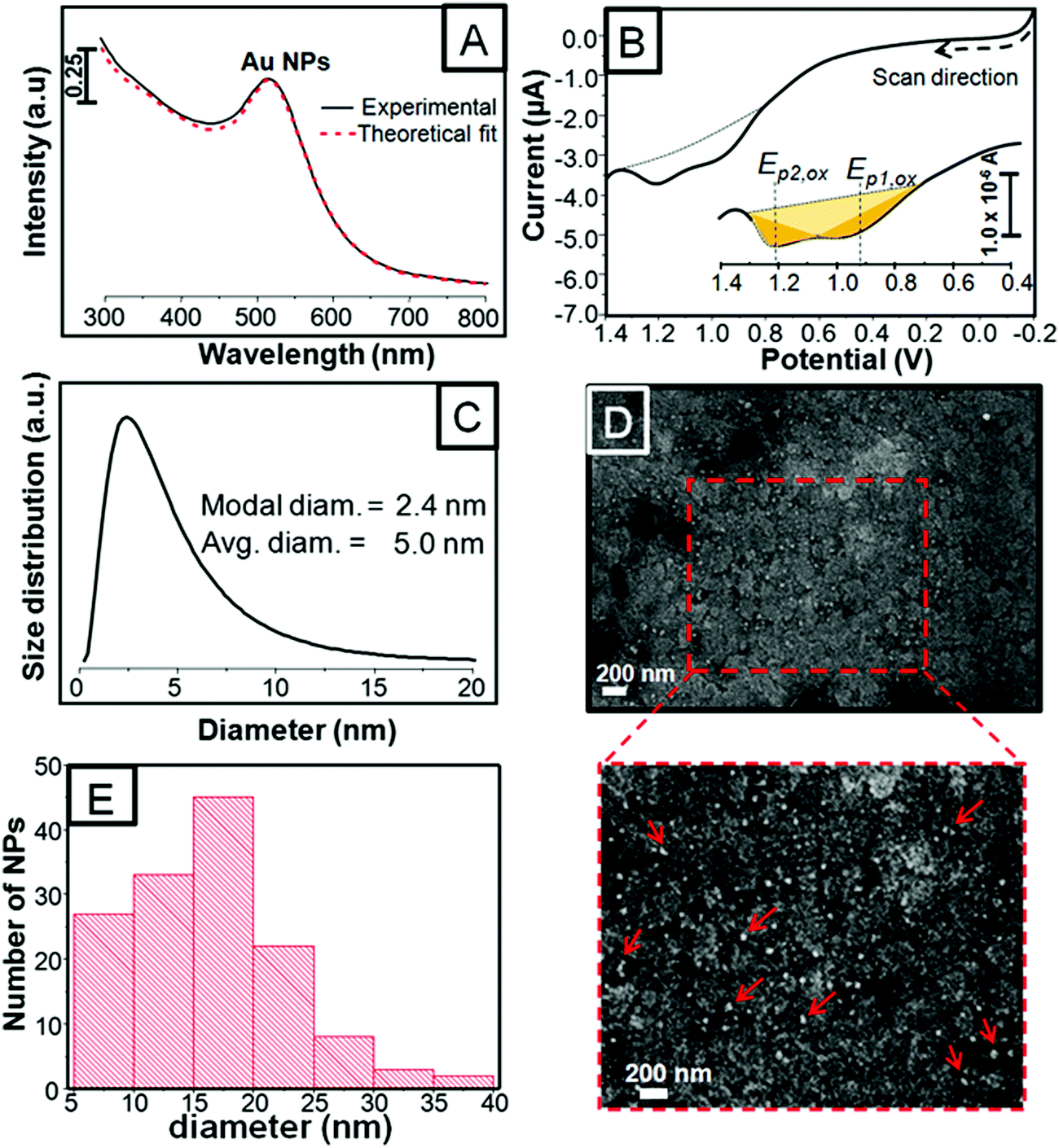 | ||
| Fig. 1 UV-vis extinction spectrum of the as-synthesized citrate-coated Au NPs along with a red dashed curve that represents the theoretical fit obtained by optical extinction spectroscopy (OES) (A). Linear scan voltammetry (LSV) of the as-deposited (EPD 600 s) citrate-coated Au NPs on the ITO/glass electrode in 0.1 M KClO4 plus 0.01 M KBr at a scan rate of 0.01 V s−1 (B). OES calculation indicating 2.4 and 5.0 nm modal and average diameters of Au NPs in solution, respectively (C). Inset shows a zoomed-in image of the LSV curve with a shaded area under the oxidation peak. SEM image of the as-deposited Au NPs on ITO/glass along with a zoomed-in area marked with a red dotted line (D). Histogram constructed from the zoomed-in SEM image (E). Red arrows point out the islands comprising three or four NPs. | ||
We recently performed the same synthesis of citrate-coated Au NPs and observed two similar size populations and two distinct oxidation peaks obtained by OES and LSV; however, Ep,ox appeared more negative.43 In addition, the LSV curve in Fig. 1B shows a remarkable increase in current starting at 0.7–0.8 V and two peaks that seem to overlap. Such positive shifts in potential and some of the aforementioned LSV profiles can be associated with NP agglomeration caused by evaporation of ethanol used as the solvent for the MB dye. Allen et al. studied Au NS agglomerations by monitoring changes in UV-vis spectroscopy, SEM, and LSV.23 They synthesized citrate-coated 4, 15, and 50 nm diam. Au NSs and varied the pH from 9 to 1.8 in order to follow the different stages of agglomeration to finally conclude that the oxidation peaks showed more positive shifts consistent with the formation of agglomerates. For the small size NSs (4 and 15 nm), there were always two overlapped LSV peaks that appeared between 0.7 and 1.0 V attributed to the isolated and aggregated Au NPs, respectively. They also determined that the maximum shift in potential for Au NPs of 15 nm at the lowest pH was limited by the oxidation potential of bulk Au at ∼0.9 V. Surprisingly, our LSV peak, Ep2,ox, compared to theirs appeared even more positive (at ∼1.2 V) than that of dissolution of bulk Au, while Ep1,ox appears at the potential at which high agglomerates were observed by Allen.23 The LSV profiles are similar because both peaks are somehow overlapped. Positive shifts in potential were also studied later by Pattadar et al., who demonstrated that the EPD of Au NSs on bare ITO electrodes required a higher overpotential to be oxidized as compared to the same NPs deposited on electrostatically-modified electrodes (i.e., APTES).24 In conclusion, our results indicate that more positive potentials are needed for oxidation of Au NPs, which can be attributed to a combination of elements associated with the formation of agglomerates in the first place, the deposition method (EPD), and the adsorption of MB onto Au NPs.44
EPD of Au NPs on graphene/ITO/glass
Fig. 2A shows a selected LSV curve obtained from the as-deposited and as-treated Au NPs on G/ITO/glass. It should be pointed out that CVD graphene (G) was transferred to the ITO/glass without the use of polymers40 (see Experimental section for more details). The SEM images in Fig. 2B–D correspond to different samples showing as-deposited citrate-coated Au NPs on as-transferred G. It should be recalled that the electrode area and the EPD and LSV parameters were kept constant during the construction of the SERS platforms. As shown in Fig. 1B, the shaded areas under the LSV peaks represent the amount of dissolved metal after anodic stripping. The LSV curve shows, from negative to positive potentials, two minor peaks and one prominent oxidation peak labeled as Ep1,ox, Ep2,ox, and Ep3,ox located at about 0.04, 0.70, and 1.10 V, respectively. The shaded areas for the two minor peaks, shown as a zoomed-in image on top of the figure, represent almost two orders of magnitude less charge (in coulombs, C) with respect to Ep3,ox (at 1.10 V). Table 1 shows the oxidation potential for each peak (Ep,ox), the calculated charge (C) under those peaks, the estimated area of metal NPs being oxidized, the total charge, and the moles of oxidized Au NPs. We assigned each Ep,ox to one particular SEM area on graphene based on the potential at which those peaks appeared and the quantity of oxidized metal. There are striking differences between the as-deposited Au NPs on ITO/glass compared to those on G/ITO/glass, as shown in Fig. 2B. First, the NPs on graphene exhibit some empty spots, isolated NPs, and the majority of agglomerated areas. For instance, the NPs highlighted with blue circles are isolated NPs aligned along the edges or defects of graphene. The defects can be distinguished by dark spots on the SEM image, which are characteristic of vacancies. This type of NP arrangement is the least frequent. The NPs inside the dotted red and the complete red circles exhibit so called “low agglomeration” and “high agglomeration” areas, which are predominant along the surface of graphene. Based on the SEM images, the peak potential, and the area under those peaks, we assigned Ep2,ox and Ep3,ox to “isolated NPs” and “low” and “high” agglomerates, marked by blue, dotted red, and red circles, as indicated in the SEM image, respectively. The peak named Ep1,ox shown in Fig. 2A (green square) will be discussed later.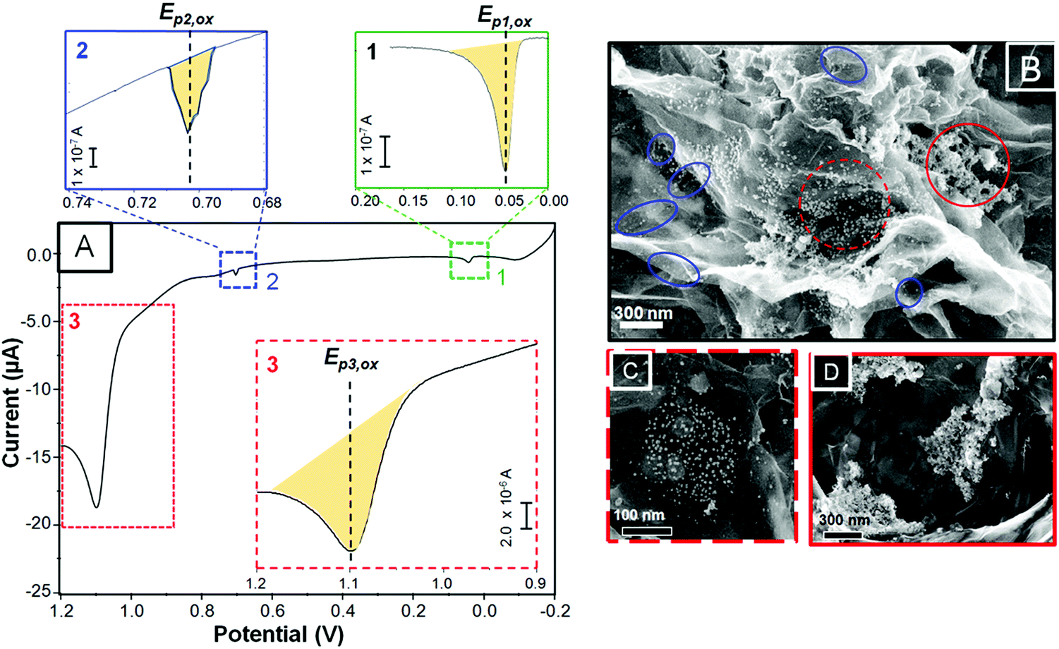 | ||
| Fig. 2 Linear scan voltammetry (LSV) of the as-deposited Au NPs on graphene previously transferred to ITO/glass (A) and the SEM images taken from different areas and magnifications of graphene (B–D). Blue, dotted red, and red circles indicate isolated Au NPs and “low” and “high” agglomerates, respectively. | ||
| EPD on graphene/ITO/glass | ||||
|---|---|---|---|---|
| Peak potential | Charge (C) | Possible SEM areaa | Total charge (C) | Total moles of Au NPs (mol) |
| a Assigned areas based on SEM, Ep,ox, and the area under the peaks. | ||||
| E p1,ox | 8.3 × 10⁻⁷ | Cu impurities? | 6.5 × 10⁻⁵ | 2.2 × 10⁻¹⁰ |
| E p2,ox | 3.3 × 10⁻⁷ | Isolated NPs | ||
| E p3,ox | 6.4 × 10⁻⁵ | Low and high agglomerates | ||
The peak potentials for Au NPs on graphene at 1.10 and 0.70 V appeared more negative (∼100–250 mV range) with respect to the peaks of the agglomerated and individual NPs, respectively, seen on ITO/glass (Fig. 1B). This indicates that despite the large agglomerates, the Au NPs dissolved at lower potentials on graphene than on ITO/glass. Brainina et al. studied the influence of different substrates on the oxidation of Au NPs by correlating the potential shifts with the Gibbs free energy. They compared NPs deposited on glassy carbon (GC) with macroscopic electrodes and demonstrated that electrooxidation of Au NPs deposited on bulky Au and Pt required higher potentials due to the stronger NP–electrode interaction. Similarly, Ag NSs deposited electrostatically on amino-terminated ITO/glass and GC-, Au- and Pt-μdiscs exhibited lower overpotentials in GC with respect to the Au and Pt electrodes.14 Our results are consistent with the literature since the GC electrode can be considered similar to our CVD graphene. With regards to the small peak seen at ∼40 mV, it is shifted way more negatively with respect to the other peaks at 1.10 and 0.7 V, indicating that the energy required to oxidize those NPs is quite insignificant. Dramatic negative shift potentials have been reported by Masitas and Zamborini, who observed a few small peaks between 0 and 400 mV for 2.5 nm diam. Au monolayer-protected clusters.15 Another possibility could be the presence of metallic impurities remaining from etching the Cu substrate with (NH4)S2O8 during the biphasic transferring procedure.40 Most related to our work is the study of Iost et al., who performed CV experiments on a graphene film after being transferred from Cu foil with ferric chloride.45 They observed a peak around 40 mV, which was assigned to anodic stripping of Cu. Our Ep1,ox peak exactly coincides with theirs, strongly suggesting that this peak can be associated with Cu impurities. It is clear that more research is needed to conclusively determine this oxidation peak.
Table 2 compares the two platforms constructed by 600 s of EPD of Au NPs on ITO/glass and G/ITO/glass. The table indicates the oxidation peaks, the current–time transient charge achieved during EPD (Fig. S1 in ESI†), the total charge under the peaks (the sum of all the areas under the peaks), and the total number of Au NPs per μm2 as measured by LSV and SEM. For the LSV technique, we considered the area under the curve (C) and the average size of the Au NPs obtained by OES (between 2.4 and 5.0 nm) to estimate the total number of NPs per area. We chose 1 μm2 because it approximates to the size of the Raman spot. There are three remarkable differences in the table. First, to the best of the LSV sensitivity, there are at least three oxidation peaks for Au NPs on graphene. Second, the coverage of NPs on graphene is six-fold larger than on ITO/glass as measured by LSV and SEM, respectively. Lastly, the total number of Au NPs per μm2 is different between LSV and SEM and between ITO and G/ITO. With regards to the latter, the discrepancy in NPs as measured by SEM (56 Au NPs per μm2) with respect to LSV (85 Au NPs per μm2) for Au NPs/ITO/glass is reasonable since some of those agglomerated NPs were counted as one large NP (20 nm diam.). The difference by a half in NPs per μm2 for graphene is also reasonable because Au NPs were counted in low agglomerated areas, as shown in Fig. 2C. High agglomerated areas were impossible to count, while individual Au NPs are not representative of the sample at all. The SEM image and histogram taken from “low agglomerates” are shown in Fig. S2 (ESI†).
| Platform | E p1,ox (V) | E p2,ox (V) | E p3,ox (V) | Transient charge during EPD (C) | Total charge under the peaks (C) | # NPs per μm2 (LSV) | # NPs per μm2 (SEM) |
|---|---|---|---|---|---|---|---|
| a # of NPs counted from SEM considering a low agglomerate (see histogram in Fig. S2, ESI) | |||||||
| Au NPs/ITO/glass | 1.21 | ∼0.96 | — | 0.12 | 1.1 × 10⁻⁵ | 85 | 56 |
| Au NPs/G/ITO/glass | 1.10 | 0.70 | 0.04 | 0.12 | 6.5 × 10⁻⁵ | 500 | ∼226a |
Deposition of metal NPs on graphitic structures was initially investigated by Penner's group, who performed electrochemical deposition experiments on HOPG substrates.28–30 By controlling the time pulse and the potential applied, they demonstrated that metal NPs can nucleate and grow preferentially at defects on HOPG, which ultimately led to the growth of mesowires as long as the length of the step edges.28 The propensity of nucleation at defect sites was explained on the basis of anodization of HOPG, which leads to oxygen-containing (surface functionalization) groups preferentially located at those defects.46 However, other groups showed that there is no need of an applied potential for nucleation and growth of metal NPs on HOPG and graphene. Lomax et al. performed electrochemistry in an open cell and observed in situ nucleation and growth of Au NPs on HOPG via AFM.34 Since the EPD process requires positive potentials, it is possible that specific areas on graphene were already oxidized prior to deposition. Therefore, it is reasonable that wrinkles, grain boundaries, and step edges on graphene may act as active sites for spontaneous deposition of negatively-charged citrate-coated Au NPs. Although more research is needed to conclusively assign each oxidation peak, at this point, the formation of large agglomerates and large coverage of Au NPs on graphene seem promising for SERS studies.
SERS of MB
SERS experiments were conducted by drop-casting (quick test) and immersing the platforms into 0.3 mM MB dissolved in ethanol (see Experimental section for more details). We first run a quick SERS test by drop-casting MB on 3 different platforms constructed by 120, 600, and 1800 s of EPD on ITO/glass in order to achieve the optimal coverage (see Experimental section for more details). Fig. 3A shows the selected Raman spectra of the four trials, which included MB on ITO/glass used as the blank. Fig. 3B presents a three-entry plot that shows Raman intensity vs. MB signal47 enhancement vs. all the trials. It is clear that 600 s of EPD outperforms SERS with respect to the other evaluated samples; however, we realized that drop casting the analyte, although it is a quick method, is not fully reliable and reproducible since the concentration of MB may be unevenly distributed along the platform. Therefore, we proceeded by immersing both platforms into the MB solution in order to let the adsorption of the dye be self-regulated. Fig. 4A shows the Raman spectra of pristine MB (used as a blank) and the as-deposited Au NPs on bare ITO/glass and G/ITO/glass immersed in MB for 10 min. Fig. 4B shows two LSV runs on the Au NPs/G/ITO/glass sample to make sure that all the Au NPs were dissolved by anodic stripping. Fig. 4C shows the Raman spectra of the G/ITO/glass sample after dissolving the already deposited Au NPs on graphene. Table 3 exhibits the MB band position, intensity, SERS of MB, and SERS after dissolving the Au NPs from the platform.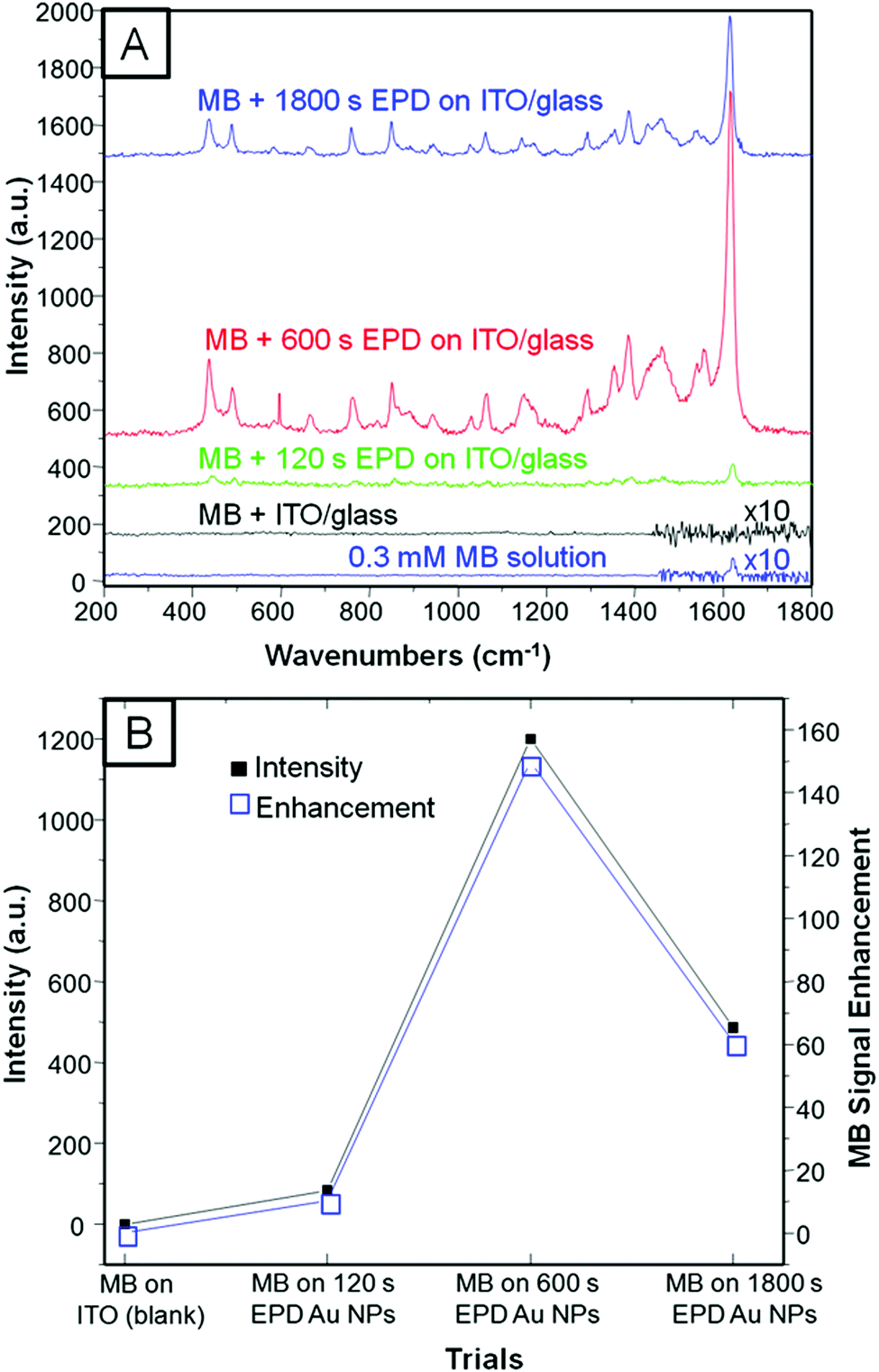 | ||
| Fig. 3 Selected Raman spectra of 0.3 mM MB blank sample and the three different quick SERS tests based on 120, 600, and 1800 s EPD of Au NPs on ITO/glass (A). Plot shows a three-entry plot of intensity vs. MB signal enhancement vs. all the trials performed in this work including the blank (B). Spectra in A are off-set for a better comparison. | ||
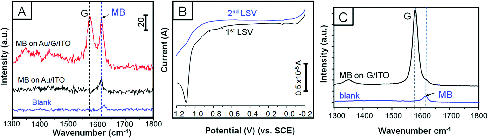 | ||
| Fig. 4 Selected Raman spectra of blank (0.3 mM MB solution) and 600 s of EPD of Au NPs on ITO/glass and G/ITO/glass after being immersed in 0.3 mM MB for 10 min (A). LSV curves showing the 1st and 2nd anodic scan from −0.2 to 1.2 V (B). Second scan confirms the disappearance of the oxidation peaks due to complete dissolution of Au. Raman spectra taken after dissolution of Au NPs from graphene and compared to the blank sample (just MB) (C). Raman spectra and LSV curves are off-set for a better comparison. | ||
| Sample | MB immersion time (min) | MB band position (cm−1) | Intensity | SERS | SERS after anodic stripping |
|---|---|---|---|---|---|
| Blank (0.3 mM MB) | — | 1624 | 8 | — | — |
| MB + Au NPs/ITO/glass | 10 | 1617 | 20 | 2.5 | Not observed |
| MB + Au NPs/G/ITO-glass | 10 | 1617 | 68 | 8.5 | Not observed |
Fig. 4A and Table 3 demonstrate that 10 min immersion of Au NPs/G/ITO is enough to achieve ∼3-fold Raman enhancement of MB with respect to Au NPs deposited on ITO/glass. The control experiment determined that MB on Au NPs/ITO/glass needs 66 h of immersion time to achieve a similar SERS performance (see Fig. S3 and Table S1, ESI†). Another control experiment demonstrated that when Au NPs are dissolved from the platform, there is no SERS at all. This clearly indicates that Au NPs are mainly responsible for SERS. Interestingly, the dissolution of Au NPs from graphene will allow reusing the platform for further EPD and SERS experiments. These experiments strongly highlight the synergy between Au NPs and graphene because the former allows SERS, while the latter causes the Au NPs to agglomerate along the wrinkles and defect areas. It is possible that the great affinity between MB and graphene44 is responsible for the improved SERS signals in such a short time.
Conclusions
In conclusion, EPD has been demonstrated to be a versatile, fast, and controllable method for constructing optimal SERS platforms. We found that the substrate plays a very important role in the EPD of citrate-coated ∼5 and ∼2.4 nm diam. Au NPs. For instance, the as-deposited Au NPs on ITO/glass appeared well-distributed along the surface, whereas the same NPs under identical EPD parameters on graphene exhibited mostly agglomerated NPs. OES, LSV, and SEM techniques were used because the former revealed two size populations from the same batch of Au NPs, whereas LSV and SEM permitted a correlation between the oxidation peaks and the different NP arrangements. By calculating the area under the oxidation peaks and the diameter of Au NPs, we were able to count how many NPs per μm2 (diameter of the laser spot) were available on each platform for SERS studies. It was determined that NP coverage on graphene was about 6× greater than on ITO/glass and the majority of those NPs appeared in the form of large agglomerates. Based on the oxidation peaks, the area under the curve, and the type of Au NPs arrangement, we were able to assign each LSV peak to a particular SEM area. A quick SERS test determined that drop-casting MB on the optimal EPD platform (600 s of EPD of Au NPs on ITO/glass) led to 1.5 orders of magnitude signal enhancement. We also tried immersion of both platforms in MB and found that G/ITO/glass immersion for 10 min was enough for an improved Raman signal similar to ITO/glass after 66 h. Dissolving the Au NPs from graphene indicated that Au NPs are mainly responsible for SERS of MB. This also indicated that the platform can be reused for further EPD and SERS analysis. The synergy between Au NPs and graphene will be further explored in the future for the design of advanced plasmonic structures.Conflicts of interest
There are no conflicts to declare.Acknowledgements
We gratefully acknowledge financial support from PICT-2016-1377, SECyT-UNC 2018–2021, and Cooperation Projects (CONICET-NSF) for student and professor exchange between the University of Louisville (KY, USA) and Universidad de La Plata. FJI thanks Prof. Frank Zamborini and his group for teaching the EPD method during one of his research visits. F. F. thanks SECyT-UNC for the doctoral fellowship. The authors thank LAMARX-SNM and LANN-SNM laboratories for their assistance with SEM and Raman spectroscopy, respectively.References
- A. Gutés,
et al., Graphene decoration with metal nanoparticles: towards easy integration for sensing applications, Nanoscale, 2012, 4, 438–440 RSC
.
- M. C. Dalfovo,
et al., Synergy between Graphene and Au Nanoparticles (Heterojunction) towards Quenching, Improving Raman Signal, and UV Light Sensing, ACS Appl. Mater. Interfaces, 2014, 6, 6384–6391 CrossRef CAS
- Z. Xiong, L. L. Zhang, J. Ma and X. S. Zhao, Photocatalytic degradation of dyes over graphene–gold nanocomposites under visible light irradiation, Chem. Commun., 2010, 46, 6099 RSC
- Y. Shi,
et al., Work Function Engineering of Graphene Electrode via Chemical Doping, ACS Nano, 2010, 4, 2689–2694 CrossRef CAS
- T. Yoon,
et al., Healing Graphene Defects Using Selective Electrochemical Deposition: Toward Flexible and Stretchable Devices, ACS Nano, 2016, 10, 1539–1545 CrossRef CAS
- L. A. Pérez,
et al., CVD Graphene Transferred with Au Nanoparticles: An Ideal Platform for TERS and SERS on a Single Triangular Nanoplate, J. Phys. Chem. C, 2016, 120, 8315–8322 CrossRef
- P. V. Kamat, Graphene-Based Nanoarchitectures. Anchoring Semiconductor and Metal Nanoparticles on a Two-Dimensional Carbon Support, J. Phys. Chem. Lett., 2010, 1, 520–527 CrossRef CAS
- M. M. Messina,
et al., Graphene Grown on Ni Foam: Molecular Sensing, Graphene-Enhanced Raman Scattering, and Galvanic Exchange for Surface-Enhanced Raman Scattering Applications, J. Phys. Chem. C, 2018, 122, 9152–9161 CrossRef CAS
- K. Xu, R. Zhou, K. Takei and M. Hong, Toward Flexible Surface-Enhanced Raman Scattering (SERS) Sensors for Point-of-Care Diagnostics, Adv. Sci., 2019, 6, 1900925 CrossRef
- S. M. Adams, S. Campione, F. Capolino and R. Ragan, Directing Cluster Formation of Au Nanoparticles from Colloidal Solution, Langmuir, 2013, 29, 4242–4251 CrossRef CAS
- L.-C. Chen, C.-T. Hsieh, Y.-L. Lee and H. Teng, Electron transport dynamics in TiO2 films deposited on Ti foils for back-illuminated dye-sensitized solar cells, ACS Appl. Mater. Interfaces, 2013, 5, 11958–11964 CrossRef CAS PubMed
- W. Chartarrayawadee, S. E. Moulton, D. Li, C. O. Too and G. G. Wallace, Novel composite graphene/platinum electro-catalytic electrodes prepared by electrophoretic deposition from colloidal solutions, Electrochim. Acta, 2012, 60, 213–223 CrossRef CAS
- O. S. Ivanova and F. P. Zamborini, Size-Dependent Electrochemical Oxidation of Silver Nanoparticles, J. Am. Chem. Soc., 2010, 132, 70–72 CrossRef CAS
- R. A. Masitas, I. V. Khachian, B. L. Bill and F. P. Zamborini, Effect of Surface Charge and Electrode Material on the Size-Dependent Oxidation of Surface-Attached Metal Nanoparticles, Langmuir, 2014, 30, 13075–13084 CrossRef CAS
- R. A. Masitas and F. P. Zamborini, Oxidation of Highly Unstable <4 nm Diameter Gold Nanoparticles 850 mV Negative of the Bulk Oxidation Potential, J. Am. Chem. Soc., 2012, 134, 5014–5017 CrossRef CAS
- R. A. Masitas, S. L. Allen and F. P. Zamborini, Size-Dependent Electrophoretic Deposition of Catalytic Gold Nanoparticles, J. Am. Chem. Soc., 2016, 138, 15295–15298 CrossRef CAS
- S. L. Allen and F. P. Zamborini, Size-Selective Electrophoretic Deposition of Gold Nanoparticles Mediated by Hydroquinone Oxidation, Langmuir, 2019, 35, 2137–2145 CrossRef CAS
- J. N. Sharma, D. K. Pattadar, B. P. Mainali and F. P. Zamborini, Size Determination of Metal Nanoparticles Based on Electrochemically Measured Surface-Area-to-Volume Ratios, Anal. Chem., 2018, 90, 9308–9314 CrossRef CAS
- D. K. Pattadar, J. N. Sharma, B. P. Mainali and F. P. Zamborini, Anodic stripping electrochemical analysis of metal nanoparticles, Curr. Opin. Electrochem., 2019, 13, 147–156 CrossRef CAS
- W. J. Plieth, Electrochemical properties of small clusters of metal atoms and their role in the surface enhanced Raman scattering, J. Phys. Chem., 1982, 86, 3166–3170 CrossRef CAS
- Kh. Z. Brainina, L. G. Galperin and E. V. Vikulova, Electrochemistry of metal nanoparticles: the effect of substrate, J. Solid State Electrochem., 2012, 16, 2357–2363 CrossRef CAS
- D. K. Pattadar and F. P. Zamborini, Halide-Dependent Dealloying of Cux/Auy Core/Shell Nanoparticles for Composition Analysis by Anodic Stripping Voltammetry, J. Phys. Chem. C, 2019, 123, 9496–9505 CrossRef CAS
- S. L. Allen, J. N. Sharma and F. P. Zamborini, Aggregation-Dependent Oxidation of Metal Nanoparticles, J. Am. Chem. Soc., 2017, 139, 12895–12898 CrossRef CAS
- D. K. Pattadar, J. N. Sharma, B. P. Mainali and F. P. Zamborini, Impact of the Assembly Method on the Surface Area-to-Volume Ratio and Electrochemical Oxidation Potential of Metal Nanospheres, J. Phys. Chem. C, 2019, 123, 24304–24312 CrossRef CAS
- D. K. Pattadar, B. P. Mainali, J. B. Jasinski and F. P. Zamborini, Electrooxidation, Size Stability, and Electrocatalytic Activity of 0.9 nm Diameter Gold Nanoclusters Coated with a Weak Stabilizer, ChemElectroChem, 2020, 7, 800–809 CrossRef CAS
- N. G. Semaltianos, E. Hendry, H. Chang and M. L. Wears, Electrophoretic deposition on graphene of Au nanoparticles generated by laser ablation of a bulk Au target in water, Laser Phys. Lett., 2015, 12, 046201 CrossRef
- X. Wang,
et al., Au nanoparticles decorated graphene/nickel foam nanocomposite for sensitive detection of hydrogen peroxide, J. Mater. Sci. Technol., 2017, 33, 246–250 CrossRef
- R. M. Penner, Mesoscopic Metal Particles and Wires by Electrodeposition, J. Phys. Chem. B, 2002, 106, 3339–3353 CrossRef CAS
- E. C. Walter,
et al., Noble and Coinage Metal Nanowires by Electrochemical Step Edge Decoration, J. Phys. Chem. B, 2002, 106, 11407–11411 CrossRef CAS
- K. H. Ng, H. Liu and R. M. Penner, Subnanometer Silver Clusters Exhibiting Unexpected Electrochemical Metastability on Graphite, Langmuir, 2000, 16, 4016–4023 CrossRef CAS
- R. J. Rice and R. L. McCreery, Quantitative Relationship between Electron Transfer Rate and Surface Microstructure of Laser-Modified Graphite Electrodes, Anal. Chem., 1989, 61, 1637–1641 CrossRef CAS
- R. J. Bowling, R. T. Packard and R. L. McCreery, Activation of highly ordered pyrolytic graphite for heterogeneous electron transfer: relationship between electrochemical performance and carbon microstructure, J. Am. Chem. Soc., 1989, 111, 1217–1223 CrossRef CAS
- E. A. Franceschini and G. I. Lacconi, Spectroelectrochemical analysis of HOPG surface controlled modification, Appl. Surf. Sci., 2017, 400, 254–261 CrossRef CAS
- D. J. Lomax and R. A. W. Dryfe, Electrodeposition of Au on basal plane graphite and graphene, J. Electroanal. Chem., 2018, 819, 374–383 CrossRef CAS
- Y. Park, J. Y. Koo, S. Kim and H. C. Choi, Spontaneous Formation of Gold Nanoparticles on Graphene by Galvanic Reaction through Graphene, ACS Omega, 2019, 4, 18423–18427 CrossRef CAS
- S. U. Yu,
et al., Simultaneous Visualization of Graphene Grain Boundaries and Wrinkles with Structural Information by Gold Deposition, ACS Nano, 2014, 8, 8662–8668 CrossRef CAS PubMed
- B. Ananthoju, R. K. Biroju, W. Theis and R. A. W. Dryfe, Controlled Electrodeposition of Gold on Graphene: Maximization of the Defect-Enhanced Raman Scattering Response, Small, 2019, 15, 1901555 CrossRef CAS PubMed
- C. J. Murphy,
et al., Anisotropic Metal Nanoparticles:
![[thin space (1/6-em)]](https://www.rsc.org/images/entities/char_2009.gif) Synthesis, Assembly, and Optical Applications, J. Phys. Chem. B, 2005, 109, 13857–13870 CrossRef CAS
Synthesis, Assembly, and Optical Applications, J. Phys. Chem. B, 2005, 109, 13857–13870 CrossRef CAS - R. Gimenez, S. Barrionuevo, C. L. A. Berli, F. J. Ibañez and M. G. Bellino, Water-graphene environment modulated by coupled nanopore interplay, Mater. Chem. Phys., 2019, 232, 382–386 CrossRef CAS
- G. Zhang,
et al., Versatile Polymer-Free Graphene Transfer Method and Applications, ACS Appl. Mater. Interfaces, 2016, 8, 8008–8016 CrossRef CAS
- D. Muñetón Arboleda,
et al., Synthesis of Ni Nanoparticles by Femtosecond Laser Ablation in Liquids: Structure and Sizing, J. Phys. Chem. C, 2015, 119, 13184–13193 CrossRef
- V. Amendola and M. Meneghetti, Size Evaluation of Gold Nanoparticles by UV-vis Spectroscopy, J. Phys. Chem. C, 2009, 113, 4277–4285 CrossRef CAS
- D. Muñeton and F. J. Ibañez, Improved Electrocatalysis and Electrophoretic Deposition due to the Strong Synergy between Au and Ag Nanoparticles, 2020, sent for publication Search PubMed.
- N. S. Kaya, A. Yadav, M. Wehrhold, L. Zuccaro and K. Balasubramanian, Binding Kinetics of Methylene Blue on Monolayer Graphene Investigated by Multiparameter Surface Plasmon Resonance, ACS Omega, 2018, 3, 7133–7140 CrossRef CAS PubMed
- R. M. Iost,
et al., Enhancing the Electrochemical and Electronic Performance of CVD-Grown Graphene by Minimizing Trace Metal Impurities, ChemElectroChem, 2014, 1, 2070–2074 CrossRef CAS
- R. J. Bowling, R. T. Packard and R. L. McCreery, Activation of Highly Ordered Pyrolytic Graphite for Heterogeneous Electron Transfer: Relationship between Electrochemical Performance and Carbon Microstructure, J. Am. Chem. Soc., 1989, 111, 1217–1223 CrossRef CAS
- R. R. Naujok, R. V. Duevel and R. M. Corn, Fluorescence and Fourier Transform surface-enhanced Raman scattering measurements of methylene blue adsorbed onto a sulfur-modified gold electrode, Langmuir, 1993, 9, 1771–1774 CrossRef CAS
Footnote |
| † Electronic supplementary information (ESI) available. See DOI: 10.1039/d0ma00333f |
| This journal is © The Royal Society of Chemistry 2020 |