DOI:
10.1039/D0MA00046A
(Paper)
Mater. Adv., 2020,
1, 1099-1112
Structural, morphological and magnetotransport properties of composite semiconducting and semimetallic InAs/GaSb superlattice structure
Received
21st February 2020
, Accepted 9th July 2020
First published on 10th July 2020
Abstract
Properties of a double-period InAs/GaSb superlattice grown by solid-source molecular beam epitaxy are presented. Precise growth conditions at the InAs/GaSb heterojunction yielded abrupt heterointerfaces and superior material quality as verified by X-ray diffraction and transmission electron microscopy (TEM) analysis. Moreover, high-resolution TEM imaging and elemental composition profiling of the InAs/GaSb heterostructure demonstrated abrupt atomic transitions between each Sb- or As-containing epilayer. An 8 × 8 k·p model is used to compute the electronic band structure of the constituent long- and short-period superlattices, taking into account the effects of conduction and valence band mixing, quantum confinement, pseudomorphic strain, and magnetic field on the calculated dispersions. Magnetotransport measurements over a variable temperature range (390 mK to 294 K) show anisotropic transport exhibiting a striking magnetoresistance and show Shubnikov-de Haas oscillations, the latter being indicative of high quality material synthesis. The measurements also reveal the existence of at least two carrier populations contributing to in-plane conductance in the structure.
Introduction
Arsenide and antimonide-based semiconductor heterostructures have attracted attention for many years as technological cornerstones for emerging, high-performance nanoscale devices.1–13 In particular, extensive research efforts have been dedicated to type-II broken-gap InAs/GaSb heterostructures8–13 wherein the superlattice (SL) periodicity can modify the band structure, resulting in either a semiconducting (energy gap, EG > 0) or semimetallic (EG ≤ 0) material system. It has been widely reported that long-period InAs/GaSb SLs exhibit semimetallic behavior whereas shorter period SLs exhibit semiconducting behavior.14–17 In the former case, two-dimensional (2D) electron and hole systems were observed in the InAs and GaSb layers, respectively, at low temperature (T). In the latter case, the formation of a minigap due to the hybridization of conduction and valence bands results in significant carrier freeze-out at low T, although higher carrier densities can appear at room temperature. Moreover, the presence of a minigap in the InAs/GaSb system has been responsible for several observations of magnetoresistance.15–17 This suggests the possibility of tuning the electronic and optical properties of the InAs/GaSb system by: (i) varying the periodicity of the SL and thereby the minigap formation;15–18 (ii) applying a hydrostatic pressure in order to modify the conduction-valence band overlap;19 (iii) adding indium (In) to the GaSb layers (i.e., InGaSb), thus further increasing the band overlap;20 (iv) utilizing different surface orientations so as to leverage their intrinsic dipole effects and further increase the band overlap,19,21 or (v) exploiting monolayer atomic stacking sequences at the InAs/GaSb heterointerfaces to change the carrier density and band overlap. It has also been reported that the InAs/GaSb interface can be designed to exhibit either an InSb-like interface or both InSb- and GaAs-like interfaces in GaSb/InSb or GaSb/GaAs-like/InAs/InSb-like/GaSb SL structures.2 In addition, the enhanced surface segregation of antimony (Sb) and In atoms, as compared to arsenic (As) and gallium (Ga), makes the InAs/GaSb heterostructure extremely challenging to realize via epitaxial growth. Moreover, this segregation effect can introduce interfacial disorder that could detrimentally affect the material's electronic properties. Thus, attaining the novel properties of an InAs/GaSb SL structure depend on the ability to grow epitaxial thin films with atomic-scale control over thickness and composition during growth. This degree of control can be achieved by molecular beam epitaxy (MBE) or metal–organic vapor phase epitaxy (MOVPE). However, despite using such techniques, interfaces with disorder, Sb segregation, and atomic intermixing have been observed in As/Sb-based SL structures grown for use in tunable-wavelength infrared imaging and low-power tunnel transistors.22–27 Therefore, in order to design application-tailored As/Sb-based devices, a precise As and Sb flux sequencing technique is necessary during the growth of InAs/GaSb heterostructures that: (i) avoids interface intermixing and atomic segregation; (ii) reduces active region defect density; (iii) lowers interface roughness; and (iv) produces interfaces free from interfacial disorder. The growth temperature, growth rate, precise and minimal V/III ratios, and appropriate shutter sequences during MBE growth are all considered as recommended solutions for achieving highly uniform and compositionally abrupt interfaces in the InAs/GaSb system.
In an InAs/GaSb broken-gap heterostructure (as shown in Fig. 1), electrons and holes are confined in the InAs and GaSb layers, respectively. However, for thin layers, quantum confinement effects can change the positions of the energy levels causing a transition from a broken-gap system to a staggered gap. By varying the thickness of the InAs/GaSb layers and hence the SL periodicity, the effective bandgap can be tuned within a well-defined range. As a result, the broken-gap band alignment leads to semimetallic behavior at long SL periodicity (where quantum confinement effects are not important), whereas for a shorter SL period quantum confinement effects become important leading to a tunable transition to a narrow-gap semiconductor. Such structures are of interest for infrared detectors,25–27 infrared emitters28,29 as well as possible spintronic applications. Moreover, in the recent surge of topological material, InAs/GaSb system is a promising platform for realizing a quantum spin Hall system and its non-trivial topological properties. Even though the current major playground lies in bilayer quantum well systems, it is natural to extend the exploration into (hybridized) SL structure and confirm their semimetallic phase, an essential ingredient in realizing topological physics.30–33 This indicates that it is essential to investigate the structural, morphological, and magnetotransport characteristics of InAs/GaSb systems with both long and short periods embedded into the same material system. Large body of transport works were devoted to either long or short period InAs/GaSb superlattice structures.14,16,34–40 In this work, we present the synthesis and properties of a double period SL consisting of a short-period SL of 10 InAs/GaSb repeats embedded into a long-period SL of 4 InAs/GaSb repeats, grown by solid-source MBE. We correlate results with detailed structural analysis and calculated band dispersions computed using an in-house 8 × 8 k·p framework. Within this framework, we predict the existence of a negative bandgap (−96 meV) within the long-period SL substructure and the formation of +18 meV bandgap in the short-period SL substructure. Additionally, X-ray diffraction analysis was used to evaluate the strain-state and interface quality and cross-sectional transmission electron microscopy (TEM) to study the defect and interface properties. Understanding of the magnetotransport characteristics of such complex structure is still tentative and a large body of prior work is devoted to transport in InAs/GaSb SLs.14–16 We report on the in-plane transport and magnetoresistance properties of the present InAs/GaSb heterostructure, characterized over T ≈ 390 mK up to T ≈ 294 K, and under a ±![[thin space (1/6-em)]](https://www.rsc.org/images/entities/char_2009.gif) 9 T magnetic field (B). Shubnikov-de Haas oscillations appear, testifying to the existence of high mobility carriers resulting from superior interface control. Transport is anisotropic, and a striking magnetoresistance is evident, particularly at low T. The measurements further show the existence of at least two carrier populations contributing to in-plane transport. The studies described below aim to establish pathways for InAs/GaSb-based materials for multifunctional device applications.
9 T magnetic field (B). Shubnikov-de Haas oscillations appear, testifying to the existence of high mobility carriers resulting from superior interface control. Transport is anisotropic, and a striking magnetoresistance is evident, particularly at low T. The measurements further show the existence of at least two carrier populations contributing to in-plane transport. The studies described below aim to establish pathways for InAs/GaSb-based materials for multifunctional device applications.
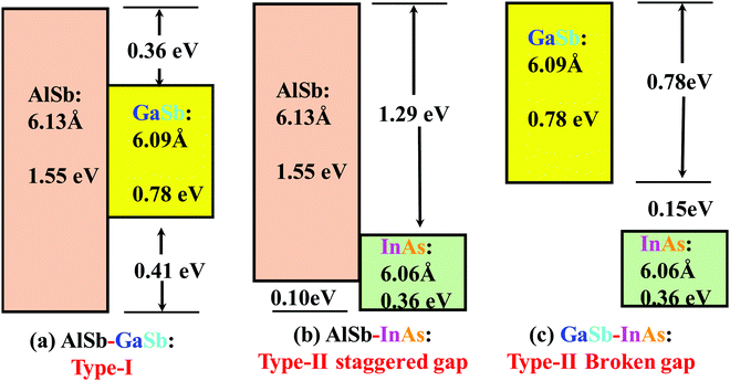 |
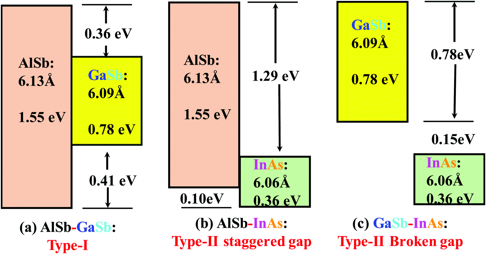
| | Fig. 1 Band lineups of AlSb–GaSb, AlSb–InAs and GaSb–InAs heterostructure. Type-I, Type-II staggered gap, and Type-II broken gap band alignments can be achieved by selecting heterostructure materials (adopted from ref. 4). | |
Experiment
The InAs/GaSb heterostructure was grown by solid-source molecular beam epitaxy (MBE) on a Wafer Technology-manufactured tellurium (Te)-doped n-type (100)GaSb substrate. A 215 nm undoped GaSb buffer layer was first grown at 500 °C, followed by the double-period InAs/GaSb SL growth using As2/In = 22, Sb2/Ga = 5 flux ratios and growth rates of ∼0.2 μm h−1 and ∼0.44 μm h−1 for InAs and GaSb, respectively. The flux ratio is referred here is the ratio between beam equivalent pressure of group-V and group-III constituents. GaSb substrate oxide desorption was performed at 600 °C under a constant Sb2 flux. The growth temperature was fixed at 500 °C during the entire growth process. The temperatures referred to in this work are the thermocouple temperatures monitored during growth. A three-zone (bulk, conductance, and cracking) antimony valved cracker source was used for the Sb2 flux during growth and oxide desorption. The cracking zone temperature was kept constant at 1000 °C whereas the bulk and conduction zone temperatures were selected based on the required flux needed during growth. Surface reconstruction patterns were repeatedly monitored in situ using reflection high energy electron diffraction (RHEED) throughout the oxide desorption process and during heterostructure growth. The thickness of each layer and the source shutter sequences were carefully selected such that the InAs/GaSb material system was internally strain-balanced. This was realized by growing an ultra-thin layer of InSb at the InAs-on-GaSb heterointerface via Sb2 soaking prior to the subsequent InAs growth step.
To determine the structural quality and relaxation state of the InAs/GaSb heterostructure, high-resolution triple-axis X-ray rocking curves and reciprocal space maps were recorded using a PANalytical X’Pert Pro system equipped with PIXcel and proportional detectors. Cross-sectional high-resolution transmission electron microscopy (HR-TEM) was used to characterize the long-range order of the SL heterostructure as well as the abruptness and uniformity of the InAs and GaSb heterointerfaces. Scanning TEM was used to capture an elemental composition profile of the complete double-period SL structure. HR-TEM imaging was performed using a JEOL 2100 transmission electron microscope. For this purpose, electron-transparent foils of thin-film cross-sections of the InAs/GaSb material stack were prepared by standard polishing techniques, i.e. mechanical grinding, dimpling and low-temperature Ar+ ion beam milling. During the TEM sample preparation process, measures were taken to prevent re-deposition of material and preparation-induced imaging artifacts due to the fragile nature of the GaSb substrate.
The heterostructure's transport and magnetotransport properties were measured across several samples using the van der Pauw technique. InSn Ohmic contacts were utilized to ensure low-resistance, stable electrical contacts at low T. Magnetotransport measurements at 390 mK and 1.1 K were performed in a 3He cryostat with the sample submerged in liquid 3He. The 3He system is equipped with a superconducting magnet, allowing B to be varied over a ±9 T range normal to the sample surface. This measurement capability has also been successfully applied to an epitaxial germanium layer heterogeneously integrated onto Si using a large bandgap composite AlAs/GaAs buffer.41T-dependent magnetotransport measurements from 4 K to 294 K in B up to ±1.4 T were performed in a closed-cycle sample-in-vapor cryostat equipped with a 1.4 T split-coil resistive magnet.
Results and discussions
A. Double-period InAs/GaSb superlattice growth
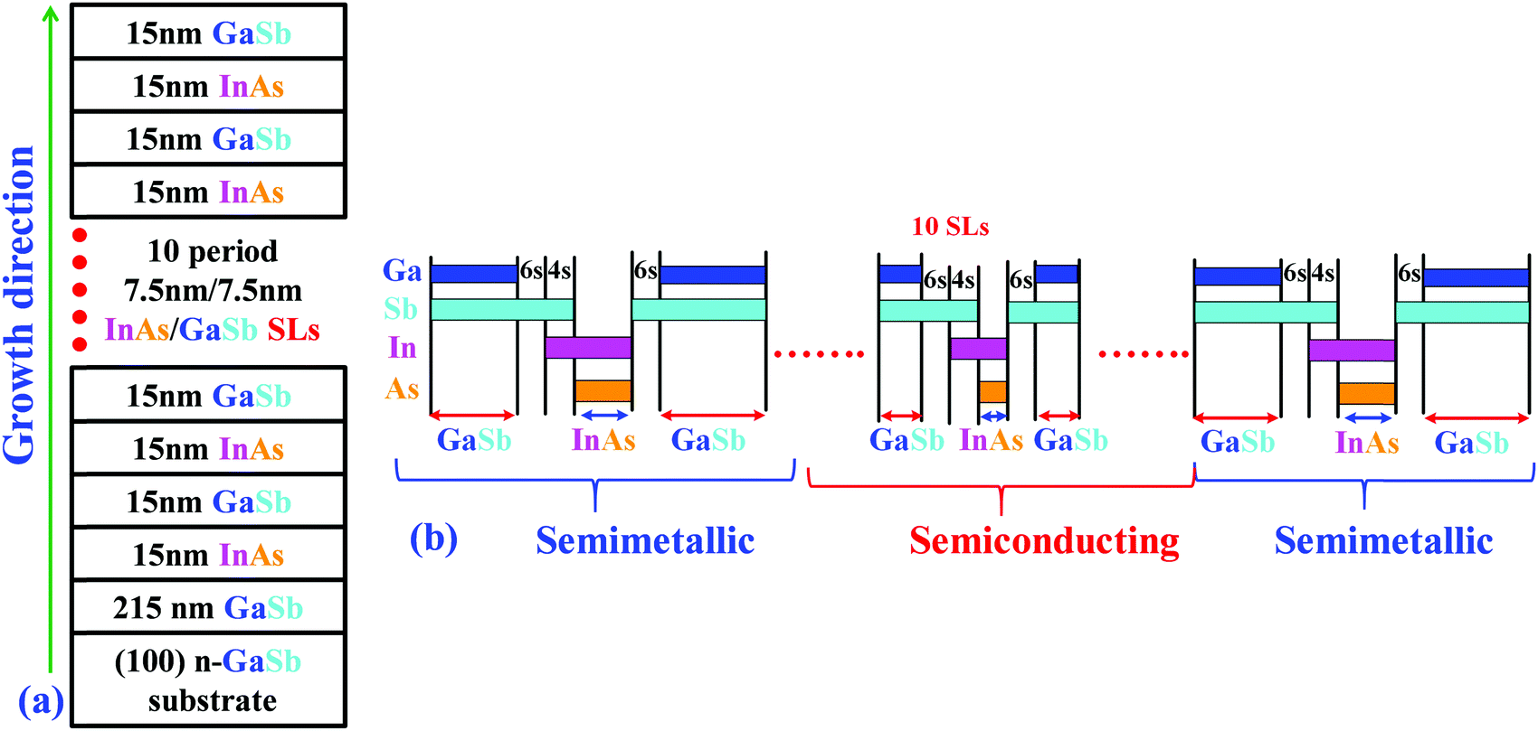
Fig. 2a shows a schematic diagram of the heterostructure studied in this work, wherein 10 repeats of 7.5 nm InAs/7.5 nm GaSb (short-period SL) were inserted between 4 repeats of 15 nm InAs/15 nm GaSb (long-period SL). The InAs/GaSb multilayer stack thus consists of the ten-period InAs/GaSb SL contained within the two top and bottom layers of the four-period InAs/GaSb SL. An equal number of tensile-strained InAs-on-GaSb interfaces and compressively-strained GaSb-on-InAs interfaces leads to an overall strain-balanced structure. The complete multi-layer structure was grown on an n-type (100)GaSb substrate by solid-source MBE using valved cracker sources for both As and Sb. Fig. 2b shows the shutter sequences used during the growth of this heterostructure. It has been reported that the InAs/GaSb SL system can exhibit a transition from semiconducting to semimetallic when the InAs layer thickness exceeds 8.5 nm.19 However, both theoretical and experimental investigations demonstrated the formation of a hybridization minigap even in the semimetallic InAs/GaSb system.14–16 The InAs layer thicknesses designed for in this study were selected to be 7.5 nm in the short-period SL structure (such that it displays semiconducting behavior with EG > 0), and 15 nm in the long-period SL structure (such that it displays semimetallic behavior with EG ≤ 0). During the growth of this structure, a GaAs-like interfacial layer at any interface (GaSb-on-InAs or InAs-on-GaSb) must be prevented.2 In the shutter sequencing during growth (Fig. 2b), the Sb2 flux was left open after the growth of GaSb. Shortly thereafter, the In flux was opened for 4 s in order to create an ultra-thin 2.13 Å InSb-like interfacial layer between the GaSb and InAs. At the GaSb-on-InAs interface, Sb2 was opened for 6 s after the InAs layer growth so as to inhibit As from escaping the surface. Furthermore, the Sb2 duration was carefully minimized such that the As2 flux in the chamber (after closing both the As needle valve and the shutter) is reduced by the cryo- and ion-pumping of the system, thereby further preventing the formation of a GaAs-like interface. Additionally, the same shutter sequence was used for both the short- and long-period InAs/GaSb SL structures. By careful control of each layer thickness and subtle control of the epitaxial InAs/GaSb heterointerface, we were able to achieve an overall strain-balanced structure. Furthermore, the InAs and GaSb layers are internally lattice matched in the growth sequence studied here, as can be observed from the X-ray analysis and by cross-sectional TEM analysis.
 |
| | Fig. 2 (a) Schematic diagram of the InAs/GaSb double SL structure, (b) MBE shutter sequence used during the growth of (a). A 2.13 Å InSb interfacial layer is incorporated at the InAs-on-GaSb heterointerface and Sb2 soaking is used at the InAs/GaSb heterointerface, respectively. An equal number of InAs and GaSb layers were selected such that the entire layer structure is strain-balanced. The same shutter sequences were used in both semimetallic and semiconducting heterointerfaces. | |
B. Strain-state investigation via X-ray diffraction
High-resolution X-ray diffraction was used to investigate the strain relaxation and heterointerface properties of the InAs/GaSb multilayer structure. Fig. 3a shows the experimental (004) X-ray rocking curve from the heterostructure described in Fig. 2a along with the simulated datasets for the (i) short-period superlattice (SPSL), (ii) long-period superlattice (LPSL), and (iii) multi-period (combination of both SP and LP superlattices) on a (001)GaSb substrate. Pendellösung oscillations and SL fringes were observed in the ω − 2θ scan, as expected for heterostructures exhibiting excellent crystalline quality and sharp, uniform heterointerfaces. As can be seen in Fig. 3a, it is not entirely accurate to ascribe the observed superlattice fringes from the multi-period superlattice heterostructure to either the short- or long-period superlattice. Rather, the experimental data is most accurately described as a convolution of the separate diffraction spectra in addition to unique diffraction features that only arise in the multi-period heterostructure. A simulated rocking curve of the same structure with an ultra-thin 2.13 Å InSb layer inserted at each InAs-on-GaSb heterointerface is shown (red) above the experimental data (blue). There is an excellent agreement between the experimental and the simulated results.
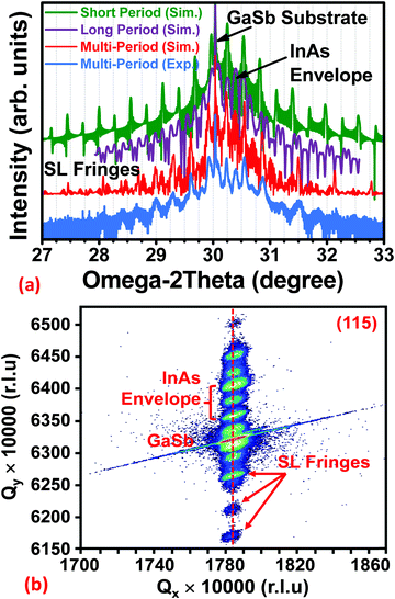 |
| | Fig. 3 (a) Symmetric experimental (004) rocking curve of the InAs/GaSb multi-layer structure (blue line), the simulated datasets for the short-period superlattice, long-period superlattice, and multi-period (combination of both short-period and long-period superlattice) rocking curve of the same (red line) with an ultra-thin 2.13 Å InSb layer at each InAs-on-GaSb heterointerface. The Pendellösung oscillations and superlattice periodicity demonstrate the superior quality of this heterostructure. (b) Asymmetric (115) reciprocal space map of the InAs/GaSb multilayer structure. All Pendellösung oscillations as well as the InAs and GaSb RLPs lie along the fully strained (vertical) line. | |
Fig. 3b shows the asymmetric (115) reciprocal space map recorded from the same structure. From Fig. 3b, one can find that the SL fringes in Fig. 3a now become contours of intensity. Both the InAs and GaSb reciprocal lattice points (RLPs) lie along a vertical line, which further confirms the balanced strain generated by the compressively-strained GaSb-on-InAs and the tensile-strained InAs-on-GaSb. Furthermore, the alignment of the GaSb substrate and InAs epilayer RLPs indicates a lack of observable lattice tilt, as expected since the entire multi-layer structure is strain balanced. We note that the lattice mismatch between InAs and GaSb is approximately 0.62%. The strain-balanced InAs/GaSb multi-layer configuration is further confirmed by cross-sectional TEM analysis below.
C. Heterointerface and compositional characterization via TEM
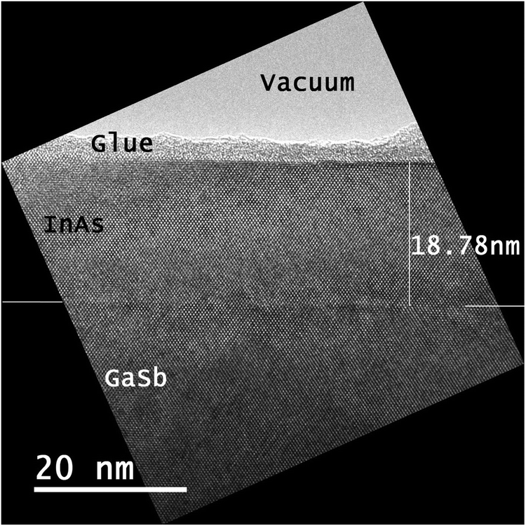
Further structural characterization of the InAs/GaSb heterostructure was performed by cross-sectional TEM measurement and analysis. Fig. 4a shows a high-resolution TEM micrograph of the InAs/GaSb multi-layer stack consisting of the ten-period InAs/GaSb SL enclosed within the top and bottom layers of the four-period InAs/GaSb SL (with two tensile-strained InAs-on-GaSb interfaces and two compressively-strained GaSb-on-InAs interfaces). In this figure, each layer and heterointerface is labeled to match the growth sequence of the multi-layer stack, as shown in Fig. 2a. Fig. 4b and c show high-resolution lattice indexing of the top four InAs and GaSb epilayers as well as the GaSb/InAs heterointerface, respectively. The TEM micrographs revealed epilayers with homogeneous and smooth heterointerfaces. One can find that there is an apparent and abrupt change in contrast (black band) between several InAs/GaSb heterointerfaces, which has been attributed to a TEM artifact. A single InAs/(001)GaSb heterostructure growth was performed and examined via cross-sectional TEM in order to conclusively demonstrate a sharp InAs/GaSb heterointerface when using the same growth parameters and shutter sequencing as for the multi-period superlattice heterostructure. Fig. 5 shows the lattice indexing of such a structure using high-resolution cross-sectional TEM. The absence of the stark contrast change (black band) and the sharp InAs/GaSb heterointerface indicates that the apparent black band is an artifact of the TEM measurement. For the InAs-on-GaSb heterointerface, an intentionally-added 4 s growth of 2.13 Å interfacial InSb was implemented in order to achieve a high quality heterointerface. Moreover, this layer aids in compensating the 0.62% tensile strain due to the lattice mismatch between InAs and GaSb. Additionally, the exposure of In and Sb fluxes at the InAs-on-GaSb heterointerface limited the As coverage, which would typically result in a deleterious GaAsSb layer. In fact, 6 s of Sb2 soaking after the InAs growth also suppressed As escape from the surface and further restricted the formation of a GaAs-like interfacial layer. Thus, both methods assisted in generating an InSb-like interfacial layer at each heterointerface and enabled superior interface control in our InAs–GaSb heterostructure.
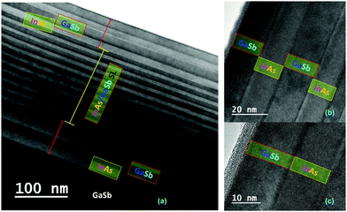 |
| | Fig. 4 (a) High-resolution cross-sectional TEM micrograph of the ten period 7.5 nm InAs/7.5 nm GaSb SL inserted between four periods of a 15 nm InAs/15 nm GaSb multilayer structure. The SL and long-period layers are labeled in this figure. (b) Lattice indexing of the top GaSb/InAs/GaSb/InAs stack as well as of part of the SL. (c) The lattice indexing of the top GaSb/InAs heterointerface. | |
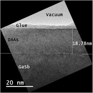 |
| | Fig. 5 High-resolution cross-sectional TEM micrograph of InAs on an n-type (100)GaSb substrate with the same InAs on GaSb shutter sequence as described in Fig. 2b. An abrupt heterointerface with the absence of an apparent black band was achieved. | |
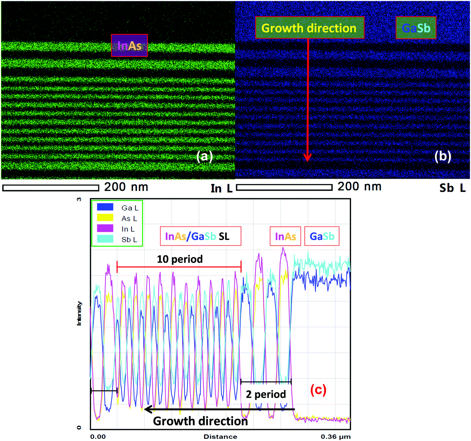
In addition, energy dispersive X-ray spectroscopy (EDS) analysis was performed on the sample during scanning (STEM) imaging in order to characterize the distribution of the elements during growth. So as to avoid re-deposition of milled material and spurious elemental distribution profiles during the analysis, the sample was carefully prepared under low-energy and low-temperature conditions. Fig. 6a and b show EDS elemental color mappings of In and Sb throughout the entire structure (previously shown in Fig. 4a), where green corresponds to the In content and blue corresponds to the Sb content. The growth direction is also included in this figure. Uniform color regions of green (In content) and blue (Sb content) in Fig. 6a and b, respectively, are clearly visible. Fig. 6c shows the EDS line profile of the same heterostructure, where each element and layer structure is clearly identified, illustrating the sharp transitions between each GaSb and InAs layer during growth. The well-defined, high-quality multi-layer structure was further investigated using computational physics to calculate the electronic band structure.
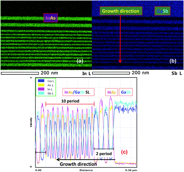 |
| | Fig. 6 (a) and (b) EDS elemental mapping of In and Sb, and (c) EDS line profile of the InAs/GaSb heterostructure. | |
D. Electronic band structure calculations via 8 × 8 k·p computational framework
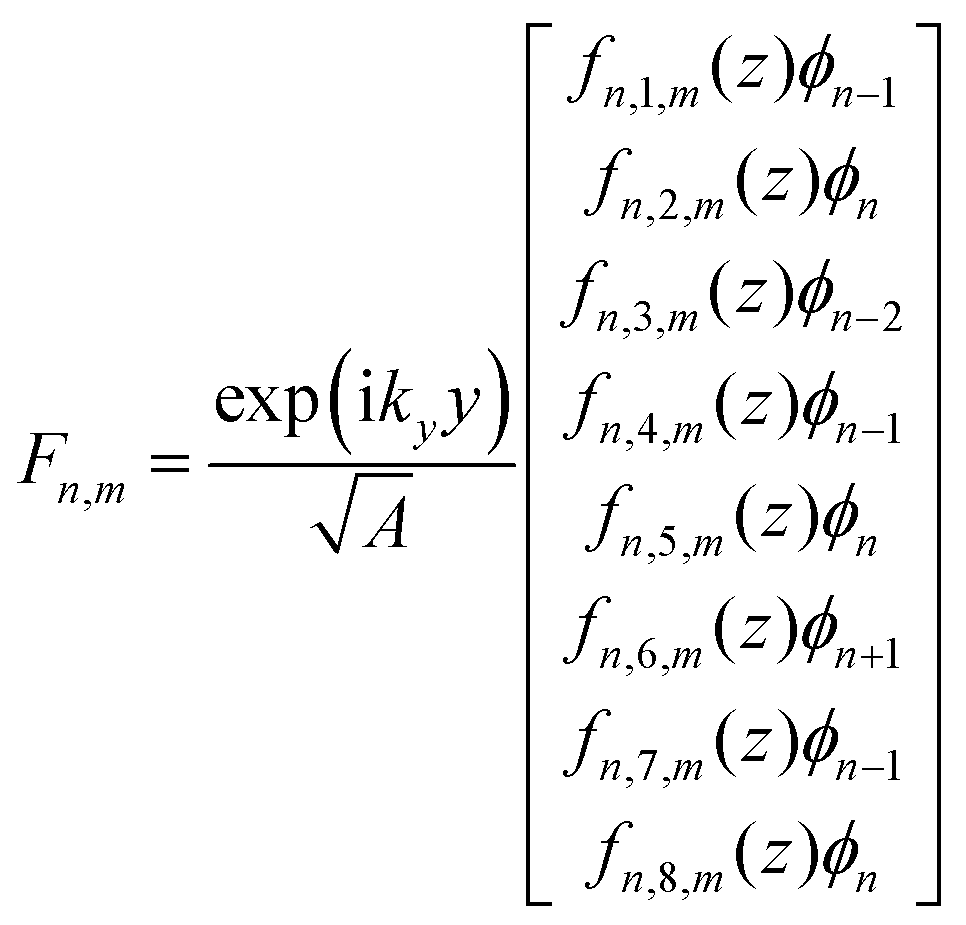
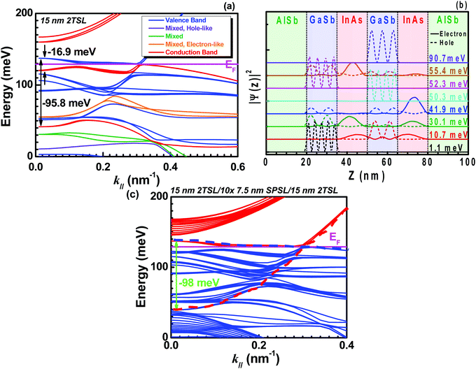
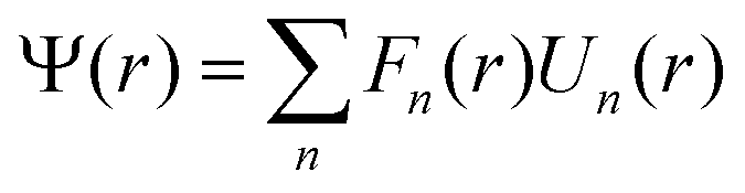
In order to determine the nature of the band structure for the as-grown long- and short-period SL substructures (i.e., semimetallic vs. semiconducting), the electronic band structures for representative InAs/GaSb heterostructures were calculated using an 8-band k·p model.34 For this purpose, we consider a two-period InAs/GaSb SL structure confined between two AlSb barrier layers. Each InAs or GaSb quantum well has an identical width, explicitly 7.5 nm or 15 nm, with the AlSb thickness selected accordingly (10 nm and 20 nm, respectively). The band dispersion calculations are based on and extend the Pidgeon-Brown (PB) Hamiltonian to include the effects of strain and the superlattice. Details of the calculation including the corresponding basis functions can be found in ref. 42. Taking the quantum confinement to be along the z direction, the kz term in the Hamiltonian is replaced by a momentum operator, while the in-plane momentum (i.e., kx, ky) remains continuous due to translational invariance. Following envelope function theory,43 the wavefunction Ψ(r) can be expanded in terms of the envelope function Fn and the Block function Un of the nth spinor:| | 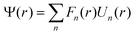 | (1) |
where Fn = exp(ikxx + ikyy)fn(z) and Un is a basis function representing the entire structure. The basis function Un here can be formulated in two different ways. Here, we follow ref. 43 and choose a material independent basis. Alternatively, one can choose a material dependent basis, as discussed in ref. 44. Within the framework of k·p theory, the envelope function can be determined by solving a set of coupled differential equations. For this work, it is assumed that all band parameters are discontinuous at each interface, which can be described by a piecewise function along the growth direction, and are taken at the limit of zero T. Likewise, the axial approximation was employed to simplify the calculations in the presence of an external B while still accounting for the valence band warping across the quantum wells.
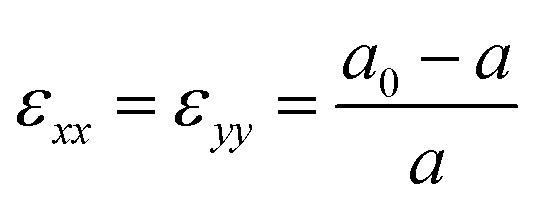
In addition to the effects of quantum confinement, the effects of pseudomorphic strain resulting from lattice-mismatch were considered using the strain Hamiltonian described in ref. 45. As the quantum wells were grown along the [001] direction, biaxial in-plane strain was assumed in the calculations. In this case, the off-diagonal elements of the strain tensor matrix are zero and the diagonal elements are 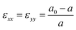 and
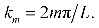
and  where a0 and a are the lattice constants of the substrate (GaSb) and layer material (InAs), respectively, and C11 and C12 are the material elastic constants. Here we take the lattice constant of GaSb for the AlSb barrier layers since the structure was grown directly on GaSb. In order to solve the set of coupled differential equations, fn(z) is expanded using a plane wave basis such that the wavefunction of the sth subband can be written as:
| |  | (2) |
where
L is the total thickness including all four quantum wells and the top and bottom AlSb barriers, and

The AlSb barrier helps to realize the Dirichlet boundary condition at finite boundary. Such expansion implies that the wavefunction is continuous across each interface. Moreover, the plane wave expansion aids in reducing the coupled differential equations to a more straightforward eigenvalue problem, which can be solved numerically, although the size of the matrix increases to (8 × (2
N + 1))
2. In this work, we let
N = 30(100) for the simplified (realistic) structure, as described in
ref. 42, which allows for convergent results while avoiding spurious solutions.
Table 1 summarizes the band and material parameters used in these calculations, which have been taken from
ref. 46.
Table 1 Summary of the band and material parameters used in this work. The parameters are taken from ref. 46
| Band parameter |
InAs |
GaSb |
AlSb |
|
m
e*(m0) |
0.024 |
0.039 |
0.14 |
|
E
g (eV) |
0.417 |
0.812 |
2.386 |
|
E
v (eV) |
−0.417 |
0.143 |
−0.237 |
|
E
p (eV) |
21.5 |
27 |
18.7 |
|
Δ (eV) |
0.39 |
0.76 |
0.676 |
|
A
c (eV nm2) |
−0.0601 |
−0.0853 |
−0.0045 |
|
γ
1
|
2.81 |
2.32 |
2.57 |
|
γ
2
|
−0.093 |
−0.842 |
−0.116 |
|
γ
3
|
0.607 |
0.458 |
0.664 |
|
κ
|
−1.060 |
−1.542 |
−0.936 |
|
a (Å) |
6.050 |
6.082 |
6.128 |
|
C
12 (GPa) |
452.6 |
402.6 |
434.1 |
|
C
11 (GPa) |
832.9 |
884.2 |
876.9 |
|
a
c (eV) |
−5.08 |
−7.5 |
−4.5 |
|
a
v (eV) |
−1 |
−0.8 |
−1.4 |
|
b (eV) |
−1.8 |
−2.0 |
−1.35 |
|
d (eV) |
−3.6 |
−4.7 |
−4.3 |
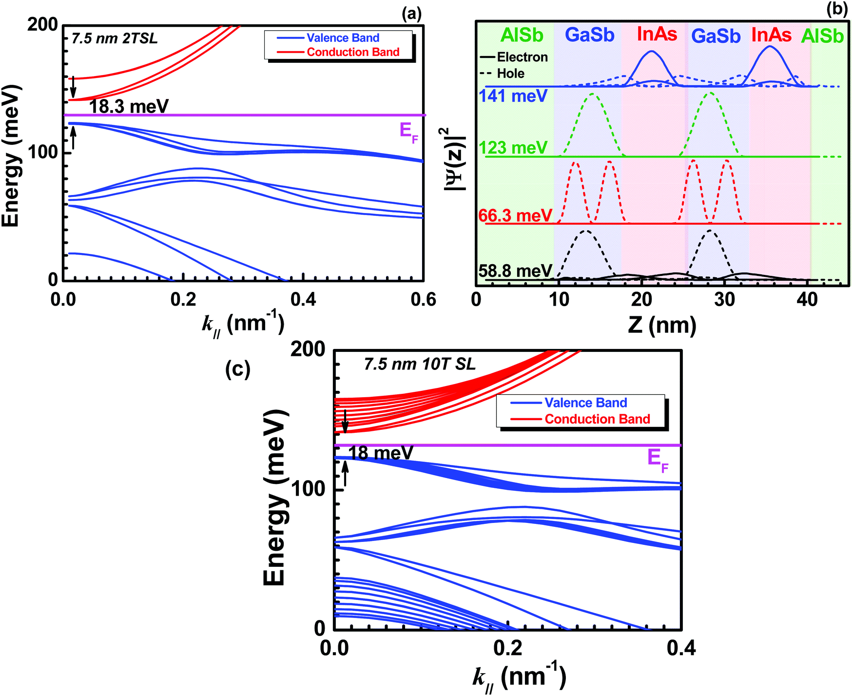
Fig. 7 shows the (a) calculated electronic band structure for the two-period 7.5 nm InAs/7.5 nm GaSb SL structure (i.e., the ‘short-period’ structure, 2T SL), (b) normalized probability density |ψ(z)|2 of the most relevant subbands, including the lowest electron and highest hole subbands, and (c) the calculated electronic band structure of 7.5 nm 10T SL, respectively. One can find from Fig. 7a that the short-period InAs/GaSb heterostructure appears to exhibit the formation of a positive gap of 18 meV at k‖ = 0 due to the strong quantum confinement present for narrow well widths. In order to verify this and correctly identify the nature of the bands in the vicinity of the Fermi level (i.e., whether they are hole- or electron-like), the occupation probabilities at k‖ = 0 of several proximate subbands are plotted in Fig. 7b. From Fig. 7b, one can find that holes (dashed lines) are preferentially confined within the GaSb quantum wells, while the confinement of the electrons (solid lines) within the InAs quantum wells is less stringent in the short-period SL structure. In this work, we assign a subband as either conduction- or valence-like based on the localization of the band's wave function at the zone center (i.e., whether the occupation probability is greater in the GaSb or InAs quantum well). The outcome of this assignment is reflected in Fig. 7a, in which the Fermi level (magenta) falls within a distinct gap between the highest hole (blue) and lowest conduction (red) subbands. The resulting energy separation was found to be approximately 18 meV in 7.5 nm 2 period or 10 period structure (Fig. 7c). As a result of the formation of a small, positive gap, the short-period SL would be expected to exhibit noticeably different magnetotransport properties at low T as compared to a semimetallic heterostructure, which will be investigated below.
 |
| | Fig. 7 (a) Calculated electronic band structure for a 7.5 nm InAs/7.5 nm GaSb two-period superlattice inserted between two 20 nm AlSb barrier layers, (b) normalized probability density |ψ(z)|2 for the zone center states of the same structure, and (c) 7.5 nm 10 period superlattice structure, respectively. A positive energy gap of ∼18 meV was extracted, indicating the formation of a normal gap under this superlattice periodicity. | |
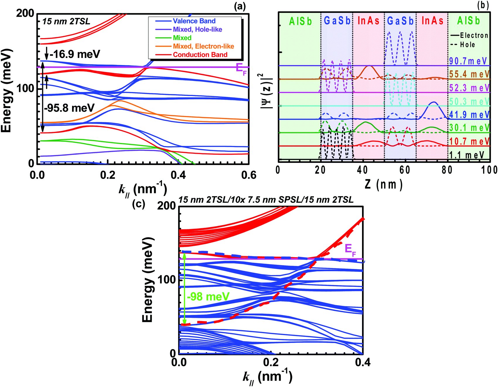
Similarly, Fig. 8 shows the (a) calculated electronic band structure for the two-period 15 nm InAs/15 nm GaSb SL structure (i.e., the ‘long-period’ structure), (b) normalized probability density |ψ(z)|2 of the most relevant subbands in proximity to the lowest conduction subband, and (c) the calculated electronic band structure of experimentally realistic 15 nm 2T SL/10 × 7.5 nm SP SL/15 nm 2T SL structure, respectively. Here, SPSL stands for short-period superlattice. Due to the complex nature of the band dispersion in Fig. 8a and difficulty in locating the lowest conduction band by inspection, the normalized probabilities plotted in Fig. 8b are in the vicinity of the lowest subband(s) with positive curvature at k‖ = 0. One can find from Fig. 8b that, unlike the short-period SL, the long-period SL band structure at k‖ = 0 contains several mixed bands extending well below the Fermi level. Following the same assignment rules presented earlier, the lowest conduction band (41.9 meV) was found to lie 95.8 meV below the top-most valence band, clearly demonstrating the effects of InAs–GaSb conduction band-valence band hybridization on the band dispersion of long-period InAs/GaSb SLs. In fact, the simulated band structure of experimentally realistic structure (Fig. 2a) exhibits the negative energy gap of ∼98 meV, where the red and blue dotted lines in Fig. 8c represents the conduction band and valence band, respectively. As the result is very close to the 15 nm 2T SL structure calculated alone (Fig. 8a), we can assume that the electrons are mostly residing in the 15 nm 2T SL structure. In addition, one can find from Fig. 8c that, for intrinsic case (no impurities added), the Fermi level lies at about 0.1288 eV and the hybridization gap was observed at about k‖ = 0.3 nm−1. Moreover, the realization of the anticrossing gap in the long-period SL structure confirms the design criteria of the multi-layer stack presented previously.
 |
| | Fig. 8 (a) Calculated electronic band structure for a 15 nm InAs/15 nm GaSb two-period superlattice inserted between two 20 nm AlSb barrier layers, (b) normalized probability density |ψ(z)|2 for the zone center states of the same structure below 100 meV, and (c) calculated band structure for grown complex 15 nm 2T SL/10 × 7.5 nm SPSL/15 nm 2T SL structure, respectively. A negative energy gap of 95.8 eV was computed, indicating the formation of an anticrossing gap and the transition from a semiconducting to semimetallic heterostructure. The red and blue dotted lines in (c) represents the conduction band and valence band, respectively. | |
E. Influence of magnetic field on calculated band structure
It should be noted that whereas the previous calculations do not consider external effects on the SL band structure, it is well-known that the formation of a minigap in InAs/GaSb heterostructures can be sensitive to external factors, e.g., applied B15–17,34 or hydrostatic pressure.19 Due to the magnitude of the minigap, it is therefore necessary to examine the impact of B on the formation or dissolution of the anticrossing gap or hybridization minigap. In order to properly account for the effect of B applied normally to the plane of the sample on the band structure, we have used the standard Peierls substitution in the Hamiltonian. Selecting the magnetic field vector potential such that A = (−By,0,0) allows for translational symmetry in the y direction to be preserved, thus ky remains a good quantum number. The differential operator is then kept for kz. The envelope functions can now be written as:| | 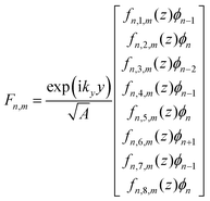 | (3) |
where the ϕn are harmonic oscillator eigenfunctions, n is the PB index, m is an index to label the energy within the same PB index in an ascending order, and A is the in-plane sample area. After replacing the in-plane momentum with annihilation and creation operators and substituting this envelope function into the Hamiltonian, the coupled differential equations are only functions of the Landau level index n and the operator kz.47 The same routine can then be carried out for the case of B = 0 T to solve the resultant set of coupled differential equations.
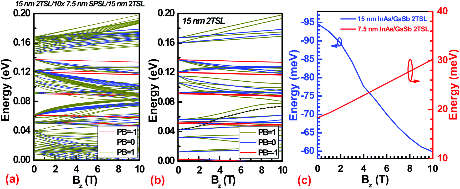
In Fig. 9a and b, we showed the Landau Levels for both the experimentally realistic and simplified structure for the low-lying PB indices. The results are qualitatively similar as expected from earlier discussion and we can gain some insight from the simplified structure. In general, we can see several fast energy increasing bands with PB = 1 (black dash line in the simplified structure result Fig. 9b) starting from ∼0.04 eV. These bands have similar magnetic field dependence as the electron bands starting around ∼0.16 eV, indicating their electronic behaviors, consistent with our previous identification of the lowest conduction bands. As magnetic field increases, these PB = 1 bands of the lowest conduction band will eventually cross the highest PB = −1 bands of the valence band and the system returns to the semiconducting phase.34 Therefore, we can define a gap in magnetic field by the difference between the highest PB = −1 bands of the valence band and the lowest PB = 1 band of the lowest conduction band. The effect of increasing B up to 10 T on the positive (negative) energy gap in the short (long)-period SL structure is depicted in Fig. 9c. One can find from Fig. 9c that although the anticrossing gap (blue) or positive gap (red) is indeed sensitive to application of B, for the SL periodicities investigated in this work, the net change in gap energy as a function of B is insufficient to cause a transition from a semimetallic to a semiconducting nature. As a result, one can expect to observe consistent magnetotransport behavior (e.g., either semimetallic or semiconducting) from both the long- and short-period SL structures for the range of experimental B studied in this work (see below).
 |
| | Fig. 9 Calculated band structure showing Landau levels for (a) experimentally realistic 15 nm 2T SL/10 × 7.5 nm SPSL/15 nm 2T SL and (b) 15 nm 2T SL structure with magnetic field Bz, respectively. (c) Energy gap as a function of magnetic field for the 7.5 nm InAs/7.5 nm GaSb (red) and 15 nm InAs/15 nm GaSb (blue) 2T SL structures. | |
F. Magnetotransport measurements of InAs-GaSb SL structure
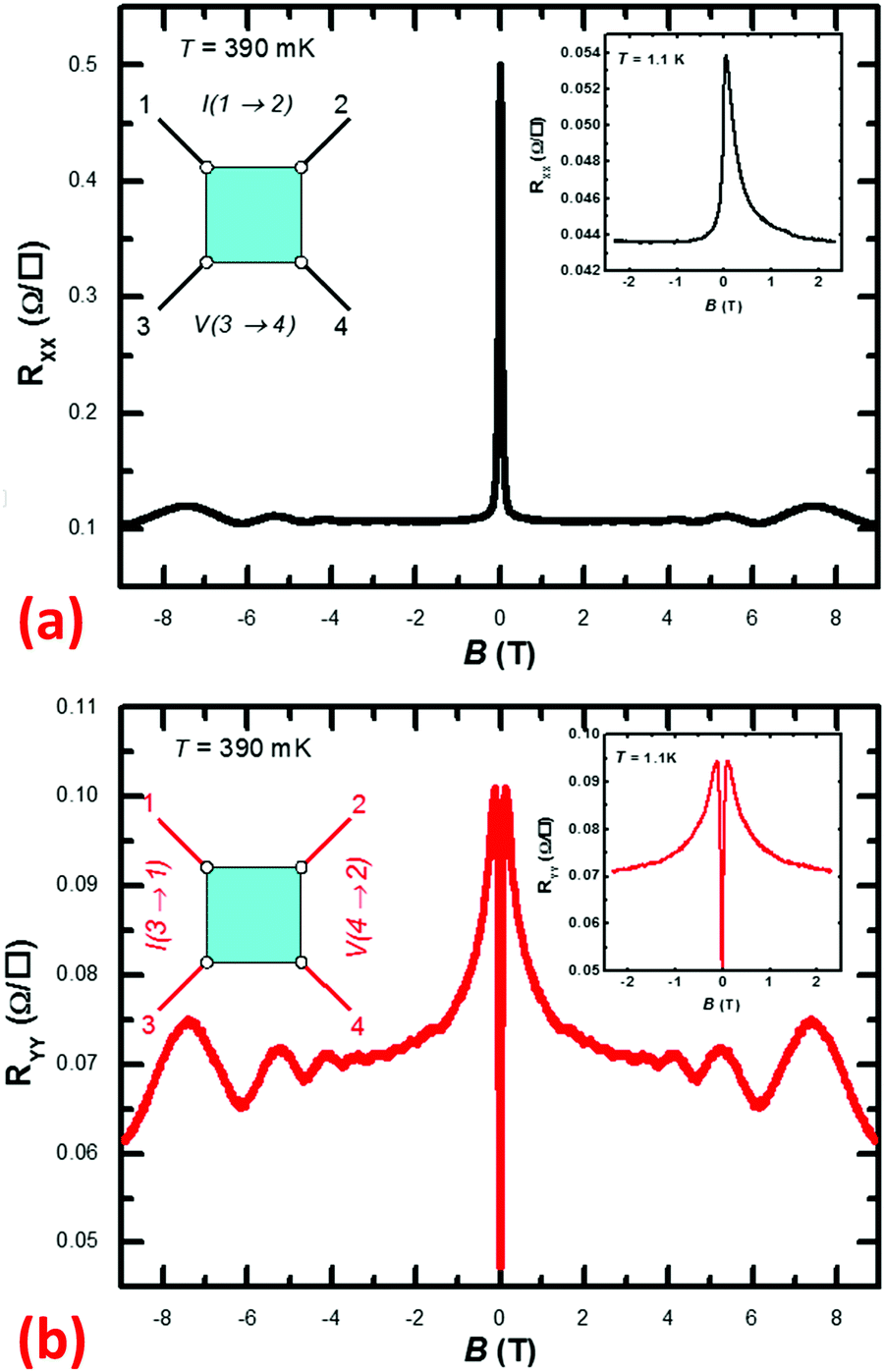
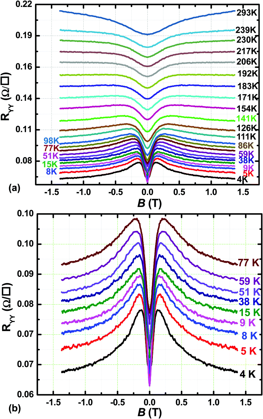
In order to explore the actual influence of B, to quantify transport coefficients, and to study the nature of the carriers in the heterostructure, magnetotransport measurements were performed in the van der Pauw geometry at T = 390 mK and T = 1.1 K up to B = 9 T, as well as over variable T (4–294 K) up to 1.4 T. B was applied normally to the plane of the sample. For all measurements, the current was applied in-plane via alloyed InSn Ohmic contacts. The following magnetotransport characteristics stand out: (i) a pronounced anisotropy between the longitudinal resistivities (i.e., the symmetric or diagonal components RXX and RYY of the magnetoresistance matrix) in the two orthogonal directions [011] and [0![[1 with combining macron]](https://www.rsc.org/images/entities/char_0031_0304.gif) 1], respectively; (ii) an abrupt magnetoresistance (dRXX/dB or dRYY/dB) that persists to high T; (iii) evidence for multicarrier transport; and (iv) an abrupt dependence on T at T ≤ 5 K. The data will be presented as experimental facts and as illustrations of the multifaceted magnetotransport the double-period InAs/GaSb SL can support, and will not at present be tied rigorously to theory. Fig. 10 shows RXX and RYY up to B = ±9 T at T = 390 mK obtained in the two orthogonal directions. Fig. 10a was obtained in the measurement orientation yielding RXX, as illustrated in the corresponding left inset, while Fig. 10b was obtained in the orientation yielding RYY, as illustrated in its corresponding left inset. The right insets show matching data obtained at T = 1.1 K. In Fig. 10a and b, Shubnikov-de Haas oscillations appear for B > 3 T (Fig. 10a) or B > 1.7 T (Fig. 10b). In Fig. 10a, prominent negative magnetoresistance was observed for B < 0.3 T, whereas in Fig. 10b, an initially positive magnetoresistance sharply transitions to negative magnetoresistance. We will return to the magnetoresistances below. A possible factor contributing to the experimentally observed anisotropy in transport properties lies in anisotropic interface strain.48 Indeed, compared to the bulk In–As and Al–Sb and Ga–Sb bonds, the interface In–Sb bonds are longer, and the Al–As and Ga–As bonds are shorter, leading to anisotropic strain at the interface. Another factor contributing to anisotropic transport may lie in small residual uniaxial strain in the structure, undetectable by structural characterization but having measurable impact on transport properties due to the sensitivity of the SL band structure and concomitant small energy gaps on any residual strain. In addition to the interface strain anisotropy mentioned above, the band structure can also bear some anisotropy between different directions at zero field, which may also contribute to the anisotropy observed in experiment as well. However, once a magnetic field is applied, the Landau Levels tend to give an “average” effect of the band structure anisotropy. Therefore, we do not expect a directional dependence in magnetic field. From the Fig. 10, we can see that the most salient anisotropy comes from the low field part (B < 1 T). The high field oscillations are similar between RXX and RYY, consistent with theoretical expectation. We note that atomic force microscopy did not reveal evidence of an anisotropic surface morphology (such as striations).
1], respectively; (ii) an abrupt magnetoresistance (dRXX/dB or dRYY/dB) that persists to high T; (iii) evidence for multicarrier transport; and (iv) an abrupt dependence on T at T ≤ 5 K. The data will be presented as experimental facts and as illustrations of the multifaceted magnetotransport the double-period InAs/GaSb SL can support, and will not at present be tied rigorously to theory. Fig. 10 shows RXX and RYY up to B = ±9 T at T = 390 mK obtained in the two orthogonal directions. Fig. 10a was obtained in the measurement orientation yielding RXX, as illustrated in the corresponding left inset, while Fig. 10b was obtained in the orientation yielding RYY, as illustrated in its corresponding left inset. The right insets show matching data obtained at T = 1.1 K. In Fig. 10a and b, Shubnikov-de Haas oscillations appear for B > 3 T (Fig. 10a) or B > 1.7 T (Fig. 10b). In Fig. 10a, prominent negative magnetoresistance was observed for B < 0.3 T, whereas in Fig. 10b, an initially positive magnetoresistance sharply transitions to negative magnetoresistance. We will return to the magnetoresistances below. A possible factor contributing to the experimentally observed anisotropy in transport properties lies in anisotropic interface strain.48 Indeed, compared to the bulk In–As and Al–Sb and Ga–Sb bonds, the interface In–Sb bonds are longer, and the Al–As and Ga–As bonds are shorter, leading to anisotropic strain at the interface. Another factor contributing to anisotropic transport may lie in small residual uniaxial strain in the structure, undetectable by structural characterization but having measurable impact on transport properties due to the sensitivity of the SL band structure and concomitant small energy gaps on any residual strain. In addition to the interface strain anisotropy mentioned above, the band structure can also bear some anisotropy between different directions at zero field, which may also contribute to the anisotropy observed in experiment as well. However, once a magnetic field is applied, the Landau Levels tend to give an “average” effect of the band structure anisotropy. Therefore, we do not expect a directional dependence in magnetic field. From the Fig. 10, we can see that the most salient anisotropy comes from the low field part (B < 1 T). The high field oscillations are similar between RXX and RYY, consistent with theoretical expectation. We note that atomic force microscopy did not reveal evidence of an anisotropic surface morphology (such as striations).
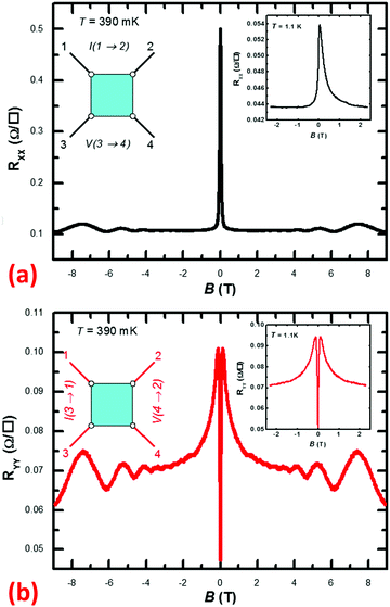 |
| | Fig. 10 (a) In-plane longitudinal resistivity (component RXX of the magnetoresistance matrix) vs. B, up to B = ±9 T, obtained at T = 390 mK. The left inset shows the measurement configuration. The right inset shows RXX at T = 1.1 K over B = ±1.4 T. A large negative magnetoresistance is observed for |B| < 0.3 T, which is reduced at T = 1.1 K (inset) compared to T = 390 mK (main panel). For B > 2.5 T, Shubnikov-de Haas oscillations appear. (b) In-plane longitudinal resistivity in the direction orthogonal to panel (a) (component RYY) vs. B, up to B = ±9 T, obtained at T = 390 mK. The left inset shows the measurement configuration. The right inset shows RYY at T = 1.1 K over B = ±1.4 T. The abrupt magnetoresistance is reduced at T = 1.1 K (inset) compared to T = 390 mK (main panel). For B > 1.7 T, Shubnikov-de Haas oscillations again appear, testifying of a carrier population with high mobility. | |
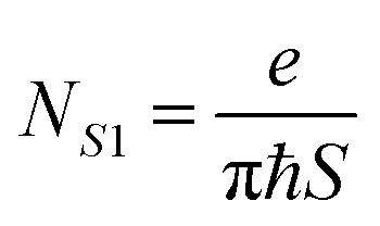
From the Shubnikov-de Haas oscillations, which are due to the quantization of energy levels into discrete Landau levels, the size of the Fermi surface of the carrier population responsible for the oscillations (and hence their areal density NS1) can be obtained. By plotting the location (in 1/B) of the maxima of the RXX oscillations vs. their index (with an arbitrary offset), as shown in Fig. 11, we obtain a slope S = 0.0527 T−1. Assuming that the Zeeman energy spin splitting is not resolved, as no splitting is observed in the Shubnikov-de Haas oscillations, S is then related to NS1 by:
| |  | (4) |
where
ħ denotes Planck's constant, and
e the elementary charge. Using
eqn (4), we find
NS1 = 9.20 × 10
15 m
−2. Given the carrier density
NS1, the calculate Fermi level lies at 0.1295 eV (0.1283 eV) for electron (hole)-doped cases. Shubnikov-de Haas oscillations require minimal disorder-induced Landau level broadening, implying that the carrier population giving rise to the oscillations has a substantial carrier mobility. From the value of the magnetic field
B0 where Shubnikov-de Haas oscillations just become visible, we can extract an estimate of mobility
μ. The onset of visibility of the oscillations occurs at
μB0 ≈ 1. With
B0 ≈ 1.7 T (
Fig. 10b), we find the estimate
μ ≈ 5900 cm
2 V
−1 s
−1 at
T = 390 mK (compared also below).
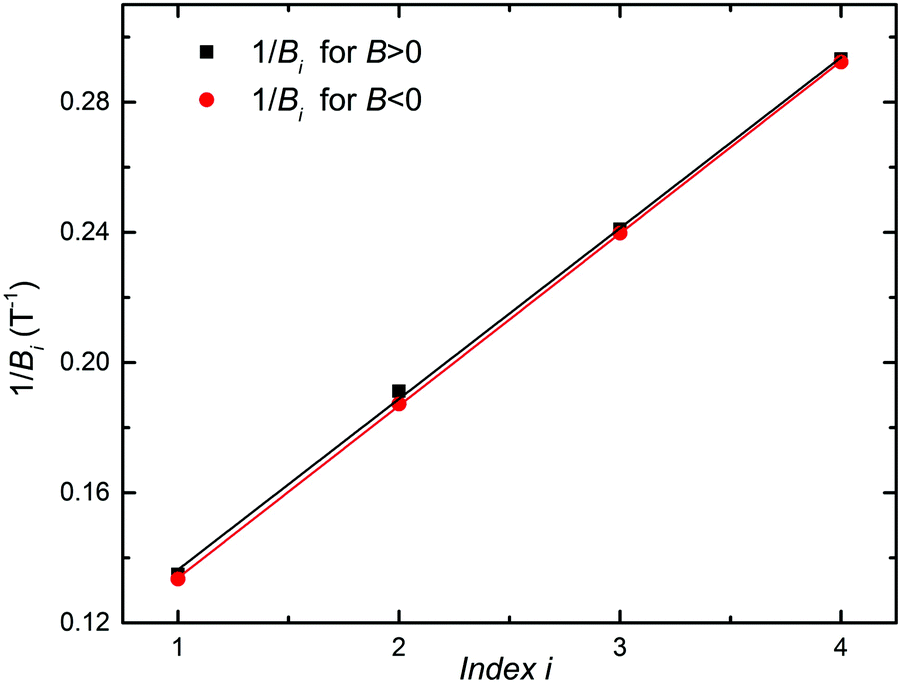
Fig. 12 depicts the Hall resistance (
i.e., the antisymmetric or off-diagonal component of the magnetoresistance matrix)
RXY up to
B = ±9 T at
T = 390 mK (main panel) and up to
B = ±1.4 T at
T = 4–294 K (inset). For
B > 0.3 T,
RXY is linear in
B, while for
B < 0.3 T sharp deviations from linearity arise. While multicarrier effects
49 are a possible origin of nonlinear
RXY, in the present van der Pauw geometry it is more plausible that the features for
B < 0.3 T in
RXY result from intermixing of
RXX and/or
RYY into the measurement of
RXY. Indeed the range in
B of the nonlinearity coincides with the range over which the sharp magnetoresistance is observed. The slope reversal in
RXYvs. B at low
B (
Fig. 12) would further require at least three carrier populations to explain (two electron and one hole population), providing too many options and impacting the rigor of the analysis. A multicarrier analysis further has difficulty reproducing the abrupt behavior of
RXY at low
B and would have difficulty realistically explaining the evolution of
RXYvs. T (
Fig. 12 inset)
via the dependence on
T of three densities. Hence a more realistic and sparse explanation is provided by intermixing of
RXX and/or
RYY into
RXY, a common experimental occurrence. The slope of
RXY(
B) for
B > 0.3 T indicates that the carriers giving rise to the slope are electrons. A fit to the data in
Fig. 12 yields an areal electron density of
NS2 = 2.54 × 10
20 m
−2. Magnetotransport hence identifies two carrier populations: a population of unknown type with
NS1 = 9.20 × 10
15 m
−2 and with comparatively higher mobility, and an electron population with
NS2 = 2.54 × 10
20 m
−2, at
T = 390 mK. The
RXY data in the inset of
Fig. 12 show that at
T = 294 K,
NS2 drops to
NS2 ≈ 1.4 × 10
20 m
−2. The evolution over
T of
NS1 cannot be ascertained because Shubnikov-de Haas oscillations are a low-
T phenomenon. We now return to the estimate
μ ≈ 5900 cm
2 V
−1 s
−1 (390 mK) obtained from Shubnikov-de Haas oscillations (
Fig. 10; denoted
μ1 since it is associated with the population at density
NS1). Mobility
μ1 could in principle be derived as the ratio of the low-
B Hall coefficient (
RXY/
B) to the resistivity. Yet in the present material
RXY at low
B is obscured by intermixing of
RXX and/or
RYY into
RXY (
Fig. 12), and
RXY at higher
B characterizes a different electron population with density
NS2 as discussed above. The low-
B Hall coefficient for the population with density
NS1 is hence experimentally not available. Further, the anisotropy between
RXX and
RYY and the sharp magnetoresistance make an estimate of average resistivity uncertain. And, the existence of two carrier populations as described above makes an attribution of a resistivity associated with the population with density
NS1 alone, uncertain as well. The resistivity attributed to the population with density
NS1 is hence likewise not experimentally rigorously available. This leads to the estimate
μ1 ≈ 5900 cm
2 V
−1 s
−1 (390 mK) obtained from the Shubnikov-de Haas oscillations, which are directly attributed specifically to the population with density
NS1.
 |
| | Fig. 11 Positions in inverse B of the maxima in the Shubnikov-de Haas oscillations (Bi) for B > 0 and B < 0, vs. maxima indices (with an arbitrary offset). The slopes, identical within a small error bar, yield the areal density of the carriers responsible for the oscillations, confirming the existence of higher-mobility carriers with areal density 9.20 × 10¹⁵ m−2. | |
 |
| | Fig. 12 Hall resistance (component RXY of the magnetoresistance matrix) up to B = ±9 T, obtained at T = 390 mK. The inset shows RXY parametrized in T for 4 K ≤ T ≤ 294 K over B = ±1.4 T. Deviations from linearity of RXYvs. B are ascribed to intermixing with RXX and RYY. | |
Fig. 13 shows the evolution of RYYvs. B over 4 K ≤ T ≤ 293 K, extending the data in Fig. 10b to higher T. The positive magnetoresistance at low B persists up to 293 K, and hence cannot be attributed to antilocalization50–52 which is a low-T quantum correction to the classical resistance originating in quantum interference of time-reversed scattering trajectories. While it is tempting to attribute the positive magnetoresistance at higher T > 190 K to multicarrier conductance,49 the gradual evolution of RYYvs. B over T down to low T (where negative as well as positive magnetoresistance occurs) casts doubt over such attribution.
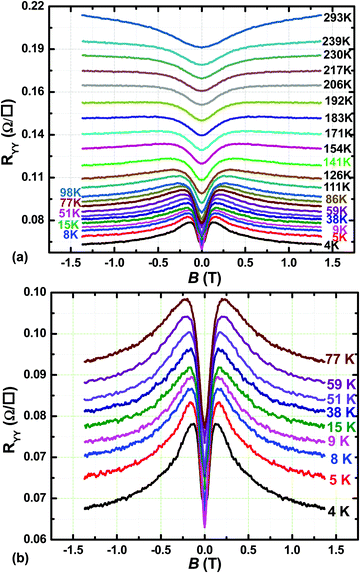 |
| | Fig. 13 (a) RYYvs. B, up to B = ±1.4 T, parametrized in T for T = 4 K to T = 293 K. (b) RYYvs. B, up to B = ±1.4 T, parametrized in T for T = 4 K to T = 77 K. The data illustrate the gradual evolution of the unique magnetoresistance with T, with magnetoresistance persisting to room temperature. | |
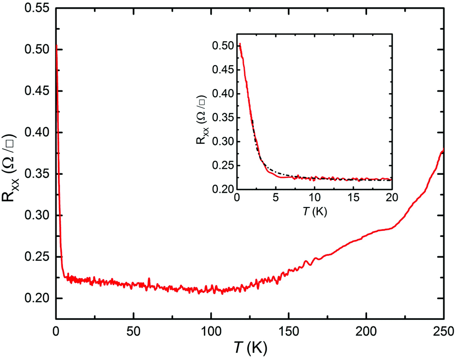
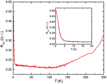
Fig. 14 shows the dependence on T of RXX from 380 mK to 250 K at B = 0 T. The inset displays the dependence on T of RXX for 380 mK < T < 20 K. For 100 K < T < 250 K, the behavior is, as expected for a high quality heterostructure, metallic due to the reduction of phonon scattering upon lowering T. For 5 K < T < 100 K, a slight rise in RXX is observed when lowering T, attributed to minor carrier freeze-out. The most salient feature is the pronounced rise in RXX for T < 5 K, illustrated in the inset, whereby RXX increases by a factor 2.2 from 5 K to 380 mK. A fit to an exponential expression assuming carrier activation across an energy gap yields a small energy gap ≈0.82 meV (corresponding to 9.5 K). Fig. 10a and its inset demonstrate that the negative magnetoresistance of RXX around B ≈ 0 T also abruptly arises with lowering T below 5 K. It is hence plausible that the same effect underlies both the rise in RXX for T < 5 K and the development of the striking magnetoresistance.
 |
| | Fig. 14 Temperature dependence of RXX for 380 mK < T < 250 K. The inset shows the dependence on T for 380 mK < T < 20 K to emphasize the pronounced rise in RXX for T < 5 K. In the inset the solid line represents data, and the dashed line a fit to activation across an energy gap. | |
Tentatively the intricate magnetoresistance in RXX and RYY and the dependence of transport and magnetotransport on T can be tied to the observation15–17,19,34,47 that anticrossing gaps and positive gaps,15,38–40 as well as several carrier populations with the potential to contribute to conductance, exist in InAs/GaSb heterostructures and are sensitive to external B.15–17,40 In the present work however, the complicated nature of the magnetoresistance, the abrupt dependence on T and the identification of at least two carrier populations defy a rigorous tie to theory. The transport and magnetotransport properties are presented as striking experimental facts observed in the double-period InAs/GaSb SL.
Conclusions
An InAs/GaSb double-period superlattice structure was grown by solid-source molecular beam epitaxy using valved cracker sources for both arsenic and antimony. The structural, morphological, and magnetotransport characteristics were investigated by high-resolution X-ray diffraction, transmission electron microscopy, and transport measurements as a function of temperature and magnetic field. Precise control of growth parameters, such as growth temperature, growth rate, and shutter sequences for the InAs/GaSb heterointerfaces, enabled the demonstration of abrupt heterointerfaces and superior material quality, as corroborated by structural and morphological analysis. The high-resolution transmission electron microscopic study and elemental composition profile of the superlattice structure revealed sharp, atomically abrupt transitions between each GaSb and InAs layer, which were realized using optimized growth parameters. An 8 × 8 k·p framework was used to compute the electronic band structures of both the long- and short-period InAs/GaSb SL substructures, yielding a negative gap of 95.8 meV and a positive gap of 18.3 meV at the zone center of each, respectively. In addition, the simulated band structure of experimentally realistic structure exhibits the negative energy gap of ∼98 meV and the result is very close to the 15 nm two-period superlattice structure calculated alone. The bandgap of each SL substructure as a function of magnetic field was calculated, demonstrating an increase (reduction) in the positive (negative) energy gap for increasing magnetic field. In-plane magnetotransport was performed over a variable temperature range, from T ≈ 390 mK to T ≈ 294 K, and in magnetic fields up to ±9 T, to investigate the carrier transport properties. Magnetotransport analysis reveals the presence of at least two carrier populations. The higher-mobility carriers exhibit Shubnikov-de Haas oscillations, testifying to the crystalline quality of the heterostructure and interfaces. Transport is anisotropic, and a striking magnetoresistance is revealed, especially at low temperature where furthermore a strong dependence of transport properties on temperature exists. The investigated epitaxial InAs/GaSb heterostructure explores the path towards future multifunctional device applications, such as infrared detectors and broken-gap tunnel field-effect transistors.
Author contributions
M. H. conceived of and supervised the research, and helped M. C. for material growth. M. C. performed the X-ray measurement and analysis. P. G. prepared the TEM sample and performed the imaging. Y. X. performed the magnetotransport measurement and Y. X. and J. J. H. analyzed the magnetotransport results. C. S., G. S., and D. S. supervised and aided in the development of several algorithms used in the k·p framework. Y. J. performed the electronic band structure calculations and analyzed the results with Z. J. M. H., J. J. H., and M. C. wrote the paper. All authors discussed the results and commented on the manuscript.
Conflicts of interest
The authors declare no competing financial interests.
Acknowledgements
M. C. acknowledges financial support from the NSF under grant number ECCS-1507950. P. G. acknowledges support from an NSF Graduate Research Fellowship. Y. J., Z. J., and D. S. are supported by the DOE under grant DE-FG02-07ER46451, and Z. J. is also supported by the NSF under grant DMR-1809120. G. D. S. and C. J. S. acknowledge support from the AFOSR through grant FA9550-17-0341. The authors also acknowledge the Institute for Critical Technology and Applied Science and Virginia Tech Nanofabrication facilities for materials characterization.
References
- Y. Zhu and M. K. Hudait, Low-power tunnel field-Effect transistors using mixed As and Sb based heterostructures, Nanotechnol. Rev., 2013, 2, 637–678 CAS.
- J.-S. Liu, Y. Zhu, P. S. Goley and M. K. Hudait, Heterointerface engineering of broken-gap InAs/GaSb multilayer structures, ACS Appl. Mater. Interfaces, 2015, 7(4), 2512–2517 CrossRef CAS PubMed.
- Y. Zhu,
et al., Role of InAs and GaAs terminated heterointerfaces at source/channel on the mixed As-Sb staggered gap tunnel field-effect transistor structures grown by molecular beam epitaxy, J. Appl. Phys., 2012, 112(2), 024306 CrossRef.
- H. Kroemer, The 6.1 Å family (InAs, GaSb, AlSb) and its heterostructures: A selective review, Physica E, 2004, 20(3–4), 196–203 CrossRef CAS.
- Y. Zhu, D. K. Mohata, S. Datta and M. K. Hudait, Reliability studies on high-temperature operation of mixed As/Sb staggered Gap tunnel FET material and devices, IEEE Trans. Device Mater. Reliability, 2014, 14(1), 245–254 CAS.
- B. R. Bennett,
et al., Antimonide-based compound semiconductors for electronic devices: A review, Solid-State Electron., 2005, 49(12), 1875–1895 CrossRef CAS.
- J. B. Boos,
et al., Sb-based n- and p-channel heterostructure FETs for high-speed, low-power applications, IEICE Trans. Electron., 2008, E91-C(7), 1050–1057 CrossRef.
- E. A. Plis, InAs/GaSb type-II superlattice detectors, Adv. Electron., 2014, 2014, 246769 Search PubMed.
- M. Razeghi and B.-M. Nguyen, Advances in mid-infrared detection and imaging: A key issues review, Rep. Prog. Phys., 2014, 77(8), 082401 CrossRef PubMed.
- M. Razeghi,
et al., Advances in antimonide-based type-II superlattices for infrared detection and imaging at center for quantum devices, Infrared Phys. Technol., 2013, 59, 41–52 CrossRef CAS.
- M. Razeghi,
et al., Antimonide-based type-II superlattice. A superior candidate for the third generation of infrared imaging systems, J. Electron. Mater., 2014, 43(8), 2802–2807 CrossRef CAS.
-
A. Rogalski, Infrared Detectors. 2nd Edition, CRC Press, New York, 2011 Search PubMed.
- in Antimonide-Related Strain-layer Heterostructures, ed. M. O. Manasreh, Gordon and Breach Science Publishers, The Netherlands, 1st Edition, 1997 Search PubMed.
- M. Altarelli, Electronic structure and semiconductor-semimetal transition in InAs-GaSb superlattices, Phys. Rev. B: Condens. Matter Mater. Phys., 1983, 28(2), 842–845 CrossRef CAS.
- M. Lakrimi,
et al., Minigaps and novel giant negative magnetoresistance in InAs/GaSb semimetallic superlattices, Phys. Rev. Lett., 1997, 79(16), 3034–3037 CrossRef CAS.
- M. J. Yang, C. H. Yang, B. R. Bennett and B. V. Shanabrook, Evidence of a hybridization gap in semimetallic InAs/GaSb systems, Phys. Rev. Lett., 1997, 78(24), 4613–4616 CrossRef CAS.
- A. Zakharova, S. Yen and K. Chao, Strain-induced semimetal-semiconductor transition in InAs/GaSb broken-gap quantum wells, Phys. Rev. B: Condens. Matter Mater. Phys., 2002, 66(8), 085312 CrossRef.
- D. M. Symons,
et al., Temperature dependence of the band overlap in the InAs/GaSb structures, Phys. Rev. B: Condens. Matter Mater. Phys., 1995, 51(3), 1729–1734 CrossRef CAS PubMed.
- S. Holmes,
et al., Magnetotransport measurements on InAs-GaSb quantum wells with the application of hydrostatic pressure, J. Phys. Chem. Solids, 1995, 56(3–4), 445–451 CrossRef CAS.
- K. S. H. Dalton,
et al., Intrinsic quantum hall effect in InAs/Ga1−xInxSb crossed gap heterostructures in high magnetic fields, Surf. Sci., 1994, 305(1–3), 156–160 CrossRef CAS.
- D. M. Symons,
et al., Orientation and pressure dependence of the band overlap in InAs/GaSb structures, Semicond. Sci. Technol., 1994, 9, 118–122 CrossRef CAS.
- J. Steinshnider,
et al., Origin of antimony segregation in GaInSb/InAs strained-layer superlattices, Phys. Rev. Lett., 2000, 85(21), 4562–4565 CrossRef CAS PubMed.
- R. M. Feenstra, D. A. Collins and T. C. McGill, Scanning tunneling microscopy of InAs/GaSb superlattices with various growth conditions, Superlattices Microstruct., 1994, 15(2), 215–220 CrossRef CAS.
- R. M. Feenstra,
et al., Interface roughness and asymmetry in InAs/GaSb superlattices studied by scanning tunneling microscopy, Phys. Rev. Lett., 1994, 72(17), 2749–2752 CrossRef CAS PubMed.
- H. J. Haugan, G. Brown and L. Grazulis, Effect of interfacial formation on the properties of very long wavelength infrared InAs/GaSb superlattices, J. Vac. Sci. Technol. B, 2011, 29(3), 03C101 CrossRef.
- D. L. Smith and C. Mailhiot, Proposal for strained type II superlattice infrared detectors, J. Appl. Phys., 1987, 62(6), 2545–2548 CrossRef CAS.
- C. Mailhiot and D. L. Smith, Long-wavelength infrared detectors based on strained InAs-Ga1−xInxSb type-II superlattices, J. Vac. Sci. Technol., A, 1989, 7(2), 445–449 CrossRef CAS.
- A. N. Baranov,
et al., Observation of room-temperature laser emission from type III InAs/GaSb multiple quantum well structures, Appl. Phys. Lett., 1997, 71(6), 735 CrossRef CAS.
- N. Deguffroy,
et al., InAs/GaSb short-period superlattice injection lasers operating in 2.5–3.5 μm mid-infrared wavelength range, Electron. Lett., 2007, 43(23), 1285–1286 CrossRef CAS.
- I. Knez, R.-R. Du and G. Sullivan, Evidence for Helical Edge Modes in Inverted InAs/GaSb Quantum Wells, Phys. Rev. Lett., 2011, 107(13), 136603 CrossRef PubMed.
- C. Liu,
et al., Quantum Spin Hall Effect in Inverted Type-II Semiconductors, Phys. Rev. Lett., 2008, 100(23), 236601 CrossRef PubMed.
- L. Du, I. Knez, G. Sullivan and R.-R. Du, Robust Helical Edge Transport in Gated InAs/GaSb Bilayers, Phys. Rev. Lett., 2015, 114(6), 096802 CrossRef PubMed.
- L. Du,
et al., Evidence for a topological excitonic insulator in InAs/GaSb bilayers, Nat. Commun., 2017, 8, 1971 CrossRef PubMed.
- Y. Jiang,
et al., Probing the semiconductor to semimetal transition in InAs/GaSb double quantum wells by magneto-infrared spectroscopy, Phys. Rev. B, 2017, 95(4), 045116 CrossRef.
- T. P. Marlow,
et al., Ground State of a Two-Dimensional Coupled Electron–Hole Gas in InAs/GaSb Narrow Gap Heterostructures, Phys. Rev. Lett., 1999, 82(11), 2362–2365 CrossRef CAS.
- C. Petchsingh, R. J. Nicholas, K. Takashina, N. J. Mason and J. Zeman, Effects of electron–hole hybridization on cyclotron resonance in InAs/GaSb heterostructures, Phys. Rev. B: Condens. Matter Mater. Phys., 2004, 70(15), 155306 CrossRef.
- C. Petchsingh, R. J. Nicholas, K. Takashina, N. J. Mason and J. Zeman, Mass enhancement and electron–hole coupling in InAs/GaSb bilayers studied by cyclotron resonance, Physica E, 2002, 12(1–4), 289–292 CrossRef CAS.
- R. J. Nicholas,
et al., Minigaps and the quantum hall effect in broken gap InAs/GaSb heterostructures, Physica B, 1998, 256–258, 207–214 CrossRef CAS.
- W. Xu, X. F. Wei and J. Zhang, Exchange-induced terahertz minigap in InAs/GaSb type II and broken-gap quantum wells, Appl. Phys. Lett., 2008, 92(16), 162108 CrossRef.
- W. Xu, P. A. Folkes and G. Gumbs, Self-consistent electronic subband structure of undoped InAs/GaSb-based type II and broken-gap quantum well systems, J. Appl. Phys., 2007, 102(3), 33703 CrossRef.
- M. K. Hudait,
et al., Magnetotransport properties of epitaxial Ge/AlAs heterostructure integrated on GaAs and silicon, ACS Appl. Mater. Interfaces, 2015, 7(40), 22315–22321 CrossRef CAS PubMed.
- J. Li and K. Chang, Spin states in InAs/AlSb/GaSb semiconductor quantum wells, Phys. Rev. B: Condens. Matter Mater. Phys., 2009, 80(3), 035303 CrossRef.
- M. G. Burt, The justification for applying the effective-mass approximation to microstructures, J. Phys.: Condens. Matter, 1992, 4(32), 6651–6690 CrossRef.
- B. A. Foreman, Envelope-function formalism for electrons in abrupt heterostructures with material-dependent basis functions, Phys. Rev. B: Condens. Matter Mater. Phys., 1996, 54(3), 1909 CrossRef CAS PubMed.
- R. M. Wood,
et al., Effects of strain and quantum confinement in optically pumped nuclear magnetic resonance in GaAs: interpretation guided by spin-dependent band structure calculations, Phys. Rev. B: Condens. Matter Mater. Phys., 2014, 90(15), 155317 CrossRef.
- I. Vurgaftman, J. R. Meyer and L. R. Ram-Mohan, Band parameters for III–V compound semiconductors and their alloys, J. Appl. Phys., 2001, 89(11), 5815–5875 CrossRef CAS.
- G. D. Sanders,
et al., Electronic states and cyclotron resonance
in n-type InMnAs, Phys. Rev. B: Condens. Matter Mater. Phys., 2003, 68(16), 165205 CrossRef.
- S. de-Leon, L. D. Shvartsman and B. Laikhtman, Band structure of coupled InAs/GaSb quantum wells, Phys. Rev. B: Condens. Matter Mater. Phys., 1999, 60(3), 1861 CrossRef CAS.
- V. Deo, Y. Zhang, V. Soghomonian and J. J. Heremans, Quantum interference measurement of spin interactions in a bio-organic/semiconductor device structure, Sci. Rep., 2015, 5, 9487 CrossRef CAS PubMed.
- G. Bergmann, Weak localization and its applications as an experimental Tool, Int. J. Mod. Phys. B, 2010, 24(12), 2015–2052 CrossRef CAS.
- R. L. Kallaher and J. J. Heremans, Spin and phase coherence measured by antilocalization in n-InSb thin films, Phys. Rev. B: Condens. Matter Mater. Phys., 2009, 79(7), 075322 CrossRef.
- R. L. Kallaher,
et al., Spin-orbit interaction determined by antilocalization in an InSb quantum well, Phys. Rev. B: Condens. Matter Mater. Phys., 2010, 81(7), 075303 CrossRef.
Footnote |
| † Correspondence and requests for materials should be addressed to M. H. |
|
| This journal is © The Royal Society of Chemistry 2020 |
Click here to see how this site uses Cookies. View our privacy policy here. 
 Open Access Article
 This Open Access Article is licensed under a Creative Commons Attribution-Non Commercial 3.0 Unported Licence
 *a,
M.
Clavel
*a,
M.
Clavel


 and
and 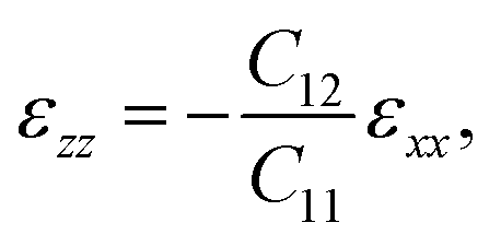 where a0 and a are the lattice constants of the substrate (GaSb) and layer material (InAs), respectively, and C11 and C12 are the material elastic constants. Here we take the lattice constant of GaSb for the AlSb barrier layers since the structure was grown directly on GaSb. In order to solve the set of coupled differential equations, fn(z) is expanded using a plane wave basis such that the wavefunction of the sth subband can be written as:
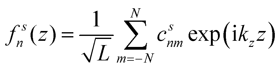
 The AlSb barrier helps to realize the Dirichlet boundary condition at finite boundary. Such expansion implies that the wavefunction is continuous across each interface. Moreover, the plane wave expansion aids in reducing the coupled differential equations to a more straightforward eigenvalue problem, which can be solved numerically, although the size of the matrix increases to (8 × (2N + 1))2. In this work, we let N = 30(100) for the simplified (realistic) structure, as described in ref. 42, which allows for convergent results while avoiding spurious solutions. Table 1 summarizes the band and material parameters used in these calculations, which have been taken from ref. 46.