
 Open Access Article
 This Open Access Article is licensed under a Creative Commons Attribution-Non Commercial 3.0 Unported Licence
A microfluidic device for both on-chip dialysis protein crystallization and in situ X-ray diffraction†
Niels
Junius‡
 a,
Sofia
Jaho
a,
Yoann
Sallaz-Damaz
a,
Franck
Borel
a,
Jean-Baptiste
Salmon
b and
Monika
Budayova-Spano
*a
a,
Sofia
Jaho
a,
Yoann
Sallaz-Damaz
a,
Franck
Borel
a,
Jean-Baptiste
Salmon
b and
Monika
Budayova-Spano
*a
aUniversité Grenoble Alpes, CEA, CNRS, IBS, F-38000 Grenoble, France
bCNRS, Solvay, LOF, UMR 5258, Univ. Bordeaux, F-33600 Pessac, France. E-mail: monika.spano@ibs.fr
First published on 5th December 2019
Abstract
This paper reports a versatile microfluidic chip developed for on-chip crystallization of proteins through the dialysis method and in situ X-ray diffraction experiments. A microfabrication process enabling the integration of regenerated cellulose dialysis membranes between two layers of the microchip is thoroughly described. We also describe a rational approach for optimizing on-chip protein crystallization via chemical composition and temperature control, allowing the crystal size, number and quality to be tailored. Combining optically transparent microfluidics and dialysis provides both precise control over the experiment and reversible exploration of the crystallization conditions. In addition, the materials composing the microfluidic chip were tested for their transparency to X-rays in order to assess their compatibility for in situ diffraction data collection. Background scattering was evaluated using a synchrotron X-ray source and the background noise generated by our microfluidic device was compared to that produced by commercial crystallization plates used for diffraction experiments at room temperature. Once crystals of 3 model proteins (lysozyme, IspE, and insulin) were grown on-chip, the microchip was mounted onto the beamline and partial diffraction data sets were collected in situ from several isomorphous crystals and were merged to a complete data set for structure determination. We therefore propose a robust and inexpensive way to fabricate microchips that cover the whole pipeline from crystal growth to the beam and does not require any handling of the protein crystals prior to the diffraction experiment, allowing the collection of crystallographic data at room temperature for solving the three-dimensional structure of the proteins under study. The results presented here allow serial crystallography experiments on synchrotrons and X-ray lasers under dynamically controllable sample conditions to be observed using the developed microchips.
Introduction
X-ray crystallography has been for many years the principal experimental technique for studying the structure of complex macromolecules such as soluble and membrane proteins. The most powerful sources for generating X-rays are synchrotrons, which have become numerous over the last few years and have increased photon flux and smaller beam size. However, the use of X-ray crystallography for the determination of the atomic structure of proteins is restricted, firstly, by the size and quality of the protein crystals. Obtaining well diffracting protein crystals with an adequate size, usually bigger than 10 μm,1 can be challenging and time-consuming. Another restrictive parameter is the radiation damage caused by the long exposure times of the protein crystals in front of the X-ray beam. To overcome this barrier, cryogenic cooling of the crystals prior to their exposure to X-ray radiation is used in order to improve the signal-to-noise ratio during the collection of the diffraction data sets. Nevertheless, the optimal cryocooling conditions need to be determined in advance for each protein since cryocooling can conceal conformational changes of the three-dimensional structure of the protein molecules.2,3 Another challenge that must be addressed during conventional X-ray crystallography experiments is sample delivery. The most widely used methods for growing protein crystals are batch crystallization and vapor diffusion. Once the protein crystals are grown to a sufficient size, they need to be harvested from the bulk and delivered in front of the X-ray beam, a process that can damage fragile samples.The direct observation and acquisition of functional conformations of proteins or other biological macromolecules remains the major goal in structural biology. Current studies focus on the use of small crystals and more challenging protein targets due to the ongoing development of increasingly bright and micro-focused synchrotron X-ray beams, as well as the emergence of X-ray free-electron lasers (XFELs). Crystals considered too small for conventional X-ray crystallography can be used for structure determination at new generation synchrotron beamlines and XFEL sources.4 Limitations related to radiation damage, long exposure times and sample manipulation can be eliminated by using serial data collection strategies.5 The use of serial synchrotron X-ray crystallography (SSX) at synchrotrons or serial femtosecond X-ray crystallography at XFELs is based on the merging of data sets collected from multiple small, isomorphous crystals.
Microfluidics may exhibit many advantages related to both the protein crystallization process and the structural X-ray analysis. First of all, setting up crystallization experiments in microfluidic devices requires minute amounts of protein samples,5 therefore reducing the production and purification costs of these high-valued biomolecules. Moreover, micro-scale geometries yield large surface area-to-volume ratios and small dimensions, enabling fine control over transport phenomena within the microfluidic structures.6,7 Microfluidic scales also limit inertial and convective phenomena,5,8 and diffusion-limited heat and mass transfer in microfluidic environments facilitates the control over temperature and concentration gradients, necessary for the growth of uniformly sized crystal populations. For all these reasons, microfluidic devices are suitable for investigating phase diagrams9–11 and performing high-throughput screening of diverse crystallization conditions by using only a few nL–μL of samples.6,11–14 Various and innovative solutions have been reported pointing out the challenges encountered while using microfluidics for investigating and screening the crystallization conditions of soluble proteins15–17 and membrane proteins.18,19
While microfluidic tools display several benefits for controlling the size uniformity and the morphology of crystals grown on microchips, the need to handle and harvest crystals prior to their use with crystallography methods has not yet been fully surpassed. The novel approach of in situ and on-chip X-ray diffraction data collection has been proposed by many groups working on the field of structural biology.5,20 Designing and fabricating microfluidic devices compatible for in situ X-ray measurements shows restrictions related to the interactions of X-rays with matter, mainly absorption and scattering. Attenuation, induced by the absorption of the material itself, must be considered since the presence of the microfluidic device adds more material in the path of the X-ray beam.8 The nature of the materials used for fabricating a microfluidic device and its thickness are highly relevant parameters since attenuation can reduce the intensity of both the incident and diffracted X-rays.5,6,8 Moreover, the thickness of the devices can severely reduce the impact of quasi-elastic scattering. Scattering effects from the materials of the device add up to X-ray scattering induced by the presence of air surrounding the experiment and/or the presence of fluids within the crystal structure and lead to increased background noise.5,6,8 Thus, decreasing the total thickness of the chip or using low density materials can moderate the impact of attenuation and scattering on the diffraction measurements. Nonetheless, decreasing the thickness of such devices also gives rise to some limitations concerning their mechanical stability and the fabrication process could be complicated.5
Microfluidic technologies have been proven crucial to couple and facilitate protein crystallization and structural studies in a single device. Many designs and materials have been proposed for in situ X-ray experiments and the following examples constitute only a small portion of available proposed solutions. PDMS-based devices using vapor diffusion21 or free interface diffusion (FID)22 have been developed for the crystallization and in situ X-ray diffraction measurements of soluble proteins. Hybrid microfluidic devices made of PDMS, COC (cyclic olefin copolymer) or PMMA (poly(methyl methacrylate))14 or PDMS and COC6 were also used to collect in situ structural data of soluble proteins and evaluate the fabrication materials for their transparency to X-rays and their contribution to the background noise. In situ data collection has been also applied in more challenging protein targets. Kisselman et al.23 developed the X-CHIP for microbatch crystallization, and Perry et al.13 fabricated a device made of thin layers of PDMS, COC and Duralar® for on-chip anomalous diffraction measurements, while Schieferstein et al.24 studied the crystallization of membrane proteins with microseeds using microchips6 made of PDMS and COC. Microfluidic chips composed of multiple levels of various fabrication materials (PDMS, COC, PMMA, graphene films or epoxy glue) can also be used for in situ X-ray data collection for serial crystallography.3,8,25
As listed above, various methods (vapor diffusion, microbatch, and free interface diffusion) have been used for the crystallization of soluble and membrane proteins on microfluidic devices and in situ X-ray diffraction experiments. High throughput screening and optimization of crystallization conditions on the microscale is another major issue that needs to be addressed. Li and Ismagilov31 published a critical and complete review on the major developments in the field of microfluidic technology for protein crystallization and high-throughput screening. They have included the milestones in microfluidic protein crystallization that have been developed and successfully tested to implement traditional crystallization methods (microbatch, vapor diffusion and free interface diffusion) in valve-, droplet- and well-based devices. Well-based microfluidic platforms are one of the most recently adapted technologies for on-chip screening of multiple crystallization conditions. Recently, Li et al.32 published their results for using a triple-gradient generator device in order to screen the conditions for crystallizing three different proteins. Droplet-based microfluidics combined with either the micro-batch crystallization method, pseudo-vapor diffusion or counter diffusion is more automated and used for setting up high-throughput screening of crystallization conditions.5,10,12,14,28 Abdallah et al.33 developed a PDMS microfluidic device in order to address the challenging problem of optimization in microfluidics. The device was used in high-throughput batch-type crystallization experiments for multi-dimensional screening and the investigation of phase diagrams of two different proteins.
Another method used in protein crystallization is dialysis. Dialysis enables precise and reversible control over the crystallization conditions9 and can be used, combined with temperature control, to decouple nucleation and crystal growth during the investigation of phase diagrams.9,28 Semipermeable membranes are used with a molecular weight cut-off (MWCO) smaller than the dimensions of the macromolecule under study, allowing small molecules, like salts or solvents, to diffuse through the membrane. Many approaches have been reported in order to integrate membranes into microfluidic chips. A review by de Jong et al.29 summarizes the integration of membranes into microfluidics in four main categories. The first method involves the direct incorporation of membranes into microfluidic devices by gluing or clamping.30 Commercially available membranes can be employed like regenerated cellulose (RC) dialysis membranes which are widely used in the crystallization of biological macromolecules. A microfluidic setup including two separate modules, a “dialysis chip” and an “exposure chip” for in situ SAXS data collection, was reported by Skou et al.40 In their dialysis chip, an RC membrane is sandwiched in-between two PDMS sheets, clamped together using two pieces of 5 mm-thick PMMA plates. Such a dialysis chip was used to concentrate a flowing protein solution using an imposed osmotic pressure difference that drives a solvent flow through the semi-permeable membrane. This dialysis chip is connected to the “exposure chip” for acquiring SAXS spectra from the osmotically-concentrated dilute protein solution.
In a previous work, we developed the prototype of an integrated apparatus for the rational optimization of crystal growth by manipulating and mapping temperature–precipitant concentration phase diagrams.9,26 The so-called crystallization bench comprises a flow cell dialysis set-up (typical volume >20 μL) to exchange conditions and control temperature during the experiments. Based on this macro scale instrument, the present work focuses on a miniaturized device that allows precise control of the experimental parameters27 exploiting the advantages of microfluidics such as the control of transport phenomena and the reduced sample volume needed per experiment (typical volume <1 μL). The new system that we developed couples microfluidics with the micro-dialysis method for on-chip crystallization of proteins and investigation of phase diagrams. The principle of the dialysis method applied to a macro scale flowing system has been discussed in our previous work.9 The novelty of our work is the use of the dialysis method on a unique versatile microfluidic device, designed to meet the requirements of both on-chip protein crystallization and in situ X-ray crystallography. Microfluidic dialysis is used here for monitoring the crystallization process in response to precipitant concentration exchange, but our microfluidic device also allows future possibilities of studying experimentally induced structural changes by serial X-ray crystallography under dynamically controlled sample conditions. We have designed a microchip for on-chip crystallization of proteins via micro-dialysis that can be set directly in front of an X-ray beam for data collection without the need for harvesting the protein crystals. Collecting data in situ prevents the modification of the environment surrounding the crystals, as it takes place in a sealed controlled volume, avoiding the degradation of the crystal quality induced by evaporation or the risk of damaging the crystals due to manual handling. We describe a microfabrication protocol to insert RC membranes in the microfluidic chip, as well as crystallization assays carried out on-chip in order to optimize the crystallization process, in situ X-ray diffraction studies and a prototype to control the temperature. Precipitant concentration is controlled via a platform for fluid handling and an interactive software interface that we designed for the preparation of the crystallization solution.9 Salts, solvents, buffers and other solutions can be pre-mixed and subsequently pumped into the microfluidic channel in a fully automated way. Uncontrolled concentration variations observed in traditional crystallization techniques due to random mixing can be eliminated. Temperature can be controlled within the microfluidic devices via a prototype using external heating through Peltier modules and copper elements (see the ESI†). Homogeneous temperature distribution or temperature gradients can be achieved across the chip. We propose a robust and inexpensive way for manufacturing numerous chips in a few hours.
Materials and methods
Microfluidic device fabrication
The fabrication of our microfluidic device is directly inspired by the protocol developed by Bartolo et al.34 for “stencil”-like micro-patterned stickers made of the thiolene-based resin NOA 81 (Norland Optical Adhesive) with soft imprint lithography. The same team (Morel et al.35) modified the original protocol in order to make photocurable resin-based microchips embedding commercial membranes to study the diffusion of various components across the membrane without applying any stress on the biological samples (cell cultures). Our microfluidic chips were made based on this pioneering work, in order to couple microfluidics with the crystallization of proteins through the dialysis method in a single device.The fabrication protocol is shown schematically in Fig. 1. The first step of the fabrication process (Fig. 1A) is photolithography where the patterns of the device are obtained on masters fabricated on silicon wafers (3 inch Si-wafers) using negative photoresist (SU-8 3000 series, Microchem). After the photolithography, the surface of both silicon wafers containing the micro patterns were treated with a vapor of HMDS (hexamethyldisilazane, Sigma Aldrich) at 95 °C for 10 min to facilitate the detachment of the PDMS stamps. The second step of the fabrication protocol consists of obtaining two PDMS (silicone elastomer base, Sylgard 184 Dow Corning or RTV-615 Momentive) stamps by replica molding of the two silicon masters. The first PDMS stamp consists of two successive layers: one layer where the microfluidic channels are located with an approximate height of 50 μm and one layer containing the pillars for the solution flow and the protein reservoir of about h = 50 μm as well. The total height of the two-layered stamp is H = 100 μm (Fig. 1A left). The second PDMS stamp consists of a single layer containing only the pillars with a total height of approximately H = 100 μm (Fig. 1A right). The total height of the patterns in each PDMS stamp is defined by the height of the respective pattern on the silicon wafers.
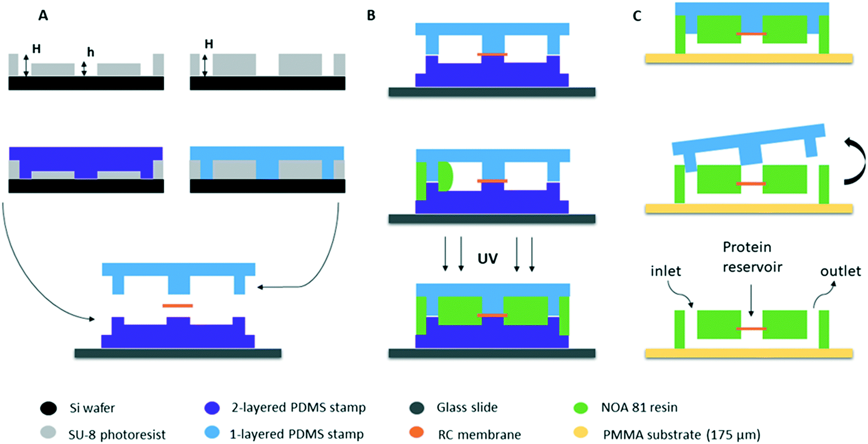 | ||
| Fig. 1 Schematic illustration of the fabrication process of the microfluidic chips embedding an RC dialysis membrane (transverse view). (A) Two silicon wafers containing the microfluidic channels and pillars are produced using negative photoresist via photolithography (top) and two PDMS stamps are made by replica molding (middle). The stamps are then supported on a glass slide, incorporating the RC dialysis membrane (bottom). The heights of the micro-patterns are H = 100 μm and h = 50 μm. (B) The space between the two PDMS stamps is filled with the photocurable resin (NOA) by capillarity (middle) and the resin is cured by UV exposure (bottom). (C) The bottom PDMS stamp is removed and the rest of the assembly (upper PDMS stamp and the partially cured NOA layer containing the RC membrane) is gently pressed on a glass slide or a 175 μm thick PMMA substrate (top). The new assembly is exposed again to UV to fully reticulate the NOA resin and the upper PDMS stamp can be finally detached (middle), revealing the micro-patterns, as the central well designed to be the protein reservoir and the inlet and outlet for the microfluidic connectors (bottom). | ||
The two-layered PDMS stamp is placed on a rigid microscope glass slide (3 in × 1 in, Dutscher) in order to enhance the support of the assembly, with the patterned channels and pillars facing upwards (Fig. 1A bottom). This way, the central pillar of the two-layered PDMS stamp which is the protein reservoir exceeds vertically by 50 μm from the horizontal surface of the stamp. A dry piece of the regenerated cellulose (RC) dialysis membrane is cut and deposited on the PDMS stamp at the exact location of the exceeding pillar (center of the stamp) which is the protein reservoir. The dialysis membranes are commercially available (Spectra/Por®) and the MWCO is defined by the molecular weight of the proteins under study. Then, the one-layered PDMS stamp has to be placed and aligned with its microstructures facing downwards. The one-layered stamp also consists of a central pillar that exceeds the surface by 100 μm and can be visually seen without any extra equipment. Therefore, the alignment can be achieved by moving the upper PDMS stamp until the central pillar of the one-layered stamp is at the exact same position as the central pillar of the two-layered stamp. This way, the dialysis membrane is “sandwiched” in between the two PDMS stamps (Fig. 1B top). The assembly is desiccated (30 min) in order to remove trapped air bubbles, to degas PDMS, and to accelerate further the insertion of the resin.
Once the alignment of the two PDMS stamps is achieved, the two pieces are kept in place simply by the good PDMS–PDMS adhesion and no external pressure or other way of bonding is applied. The empty space between the two PDMS stamps is then filled with photocurable resin NOA by capillarity (Fig. 1B). The adhesion between the two PDMS stamps prevents the liquid resin from seeping in between the pillars of the stamps. This resin has high viscosity and it takes a few minutes for NOA 81 (300 mPa s at 298 K) and NOA 61 (300 mPa s at 298 K) or approximately 30 minutes for NOA 68 (4500–5500 mPa s at 298 K) to fill the gap by capillary imbibition. No pre-treatment of the NOA resin was implemented prior to its use for the fabrication process. The commercial product was kept in a fridge at approximately 4 °C and was removed 1 or 2 hours prior to the experiment in order to reach room temperature. The resin is then cured by UV exposure through the transparent PDMS stamps (Fig. 1B bottom). We observed that the exposure settings depend on the nature of PDMS we used. In the case of Sylgard 184, the assembly was uniformly illuminated with a total deposited energy of 100 mJ cm−2 and in the case of RTV-615 the total deposited energy should be 200 mJ cm−2. These values were obtained using a UVITEC Cambridge Crosslinker at a wavelength of 365 nm. Exposure of the PDMS material to UV light can change its surface chemistry. Bhagat et al.44 used both Sylgard 184 (Dow Corning) and RTV-615 (GE Silicones) in order to directly pattern micro structures in PDMS. They prepared the PDMS mixtures by mixing the base and the curing agent in a 10![[thin space (1/6-em)]](https://www.rsc.org/images/entities/char_2009.gif) :1 (m/m) ratio and they added benzophenone, a photoinitiator used to initiate free-radical polymerization by UV light. The PDMS was directly patterned by exposure to UV light (<365 nm) at 12 mW cm−2 for 10 min and both PDMS formulas yielded the same results concerning the patterned micro structures. Our main hypothesis on this divergence in the behavior of the two PDMS types is the formula provided by the two different companies, as according to Bhagat et al.44 there should be no difference in patterning microstructures with the two types of PDMS.
:1 (m/m) ratio and they added benzophenone, a photoinitiator used to initiate free-radical polymerization by UV light. The PDMS was directly patterned by exposure to UV light (<365 nm) at 12 mW cm−2 for 10 min and both PDMS formulas yielded the same results concerning the patterned micro structures. Our main hypothesis on this divergence in the behavior of the two PDMS types is the formula provided by the two different companies, as according to Bhagat et al.44 there should be no difference in patterning microstructures with the two types of PDMS.
The first exposure allows NOA to be partially crosslinked. The gas permeability of PDMS and the inhibition of polymerization by oxygen ensure that a very thin layer of NOA in contact with the PDMS stamps on both sides remains uncured.34 The excess of NOA was cut gently from the external sides of the stamps. The top PDMS stamp with the partially cured NOA stuck on it, was removed from the bottom PDMS stamp. The upper assembly (one-layer PDMS stamp + NOA) was then gently pressed on a conventional 1 mm thick microscope glass slide or a 175 μm thick PMMA sheet (poly(methyl methacrylate), Goodfellow), as shown in Fig. 1C (top). The new assembly (glass slide or PMMA + NOA + one-layer PDMS stamp) was reticulated again at a higher energy, approximately ten times higher than the first exposure (1000 mJ cm−2 for Sylgard 184 stamps for example), leading to the adhesion of the NOA layer on the glass or PMMA substrate without any further treatment. Finally, the remaining PDMS stamp was removed (Fig. 1C). Both PDMS stamps can be re-used 4–5 times after washing with isopropanol and acetone. After using the PDMS stamps multiple times, they can be a little bit bended. This is mainly due to manipulation of the stamps. When this happens, NOA can leak between the pillars of the PDMS stamps and the stamps have to be replaced.
Following the fabrication protocol, the dialysis membrane is directly incorporated into the NOA sticker; thus no mechanical clamping or further manipulation was needed to fix the membrane on the microchip's material. Kornreich et al.30 developed a microfluidic device composed of two PDMS layers (a material widely used in microfabrication) separated by a cellulose ester dialysis membrane but the device was used only for cross polarization microscopy. Morel et al.35 also confronted the problem of multi-level clamping in PDMS, resulting in the development of a protocol using the NOA resin, for which the dialysis membrane is directly embedded into the microchip. Moreover, the permeability of PDMS to both water and air was a prohibitory factor while choosing fabrication materials, since crystallization experiments may last up to several days, as shown in Fig. 5.
Studies have been conducted to estimate the effect of UV radiation on structural and transport parameters of polymeric membranes. In the case of RC membranes, Vaquez et al.41 treated a sample with UV light at 40 W and 317 nm for 48 h in an air-circulated artificial ageing chamber. They measured a 5% increase in salt permeability (NaCl) for a UV treated sample versus an untreated sample. As suggested by Vaquez et al.,41 this result could be related to a change in the packing of the polymer chains (expansion of the polymer chains), which results in an increase of the fractional void volume in the case of UV-treated RC membranes. According to the above-mentioned studies, there is an increase of permeability of polymeric membranes after treatment with UV radiation. During the fabrication of our microchips, the RC membrane is exposed two times to UV radiation at 365 nm and the deposited energy is 100 mJ cm−2 and 1000 mJ cm−2 in the case of Sylgard 184. These exposures can be considered negligible in terms of deposited energy as compared to what has been reported in the work of Vaquez et al.41
Pictures of the microchips, micro-compartments and connectors are shown in Fig. 2. The design of the microfluidic chip proposed in this work is based on the idea of introducing the crystallization solution into a fluidic, linear channel with an automated pressure driven system and the protein solution being manually introduced by pipetting it into the protein reservoir. Both the protein reservoir and the linear channels can be distinguished from the photographs in Fig. 2A and B. During the fabrication process, the microfluidic channel is imprinted on the two-layer PDMS stamp, as shown in Fig. 1. Once the empty space between the two PDMS stamps is filled by NOA and the stamps are removed after the resin is crosslinked, the linear channel is located at the second, bottom layer of the chip (height of 50 μm) and consists of one inlet for the introduction of the crystallization solution and one outlet for the disposal of the solution (Fig. 2B). Their total height is 200 μm and they resemble holes on the photographs of the various chips (Fig. 2A and B). The reservoir designed for the deposition of the protein solution is also featured in Fig. 2A–C. The protein reservoir is the chamber located above the dialysis membrane and is imprinted on the one-layer PDMS stamp during the fabrication process (Fig. 1C bottom). The height of the protein reservoir is 100 μm and its volume differs based on the different prototypes that were designed. In Fig. 2A and B (top), a microchip containing only one reservoir for the protein solution with a maximum volume of 0.7 μL is shown. The same protein reservoir is shown in Fig. 2C. The reservoir was investigated through an optical microscope (Leica) for the alignment of the 2 layers. The piece of the RC dialysis membrane which is embedded within the microfluidic chip can be clearly distinguished in the same figure, as well as the microfluidic channels (scale 400 μm). Another chip, similar to the one illustrated in Fig. 2A and B, was designed with a maximum volume of 0.2 μL (not shown here). The microchip depicted in Fig. 2B (bottom) contains six reservoirs of 0.7 μL each for the protein solution. The objective for developing a device with six protein reservoirs is to facilitate the investigation of phase diagrams. A protein solution of constant concentration is deposited in all six reservoirs at the same time. The crystallization solution introduced in one of the linear channels has an initial concentration C1 and the solution introduced in the other channel has an initial concentration C2. The temperature of the reservoirs can be controlled by Peltier modules in pairs by supporting the chip on three different copper plates (T1, T2, and T3), as described in more details in the section for the development of the temperature control prototype (see the ESI†). In this case, six different crystallization conditions can be monitored simultaneously on one single microchip and by varying the temperature or the concentration of the crystallization solutions, more crystallization conditions can be investigated on the same device with the less possible consumption of protein sample. We study extremely slow processes that can last up to 50 days as shown in Fig. 5. Under such conditions, and because the osmotic pressure difference across the membrane is very small (dilute protein solutions), there is no significant solvent trans-membrane flux, and solute diffusion homogenizes the concentration of the crystallizing agents (salts/PEGs in our case) in the protein reservoirs connected in series.
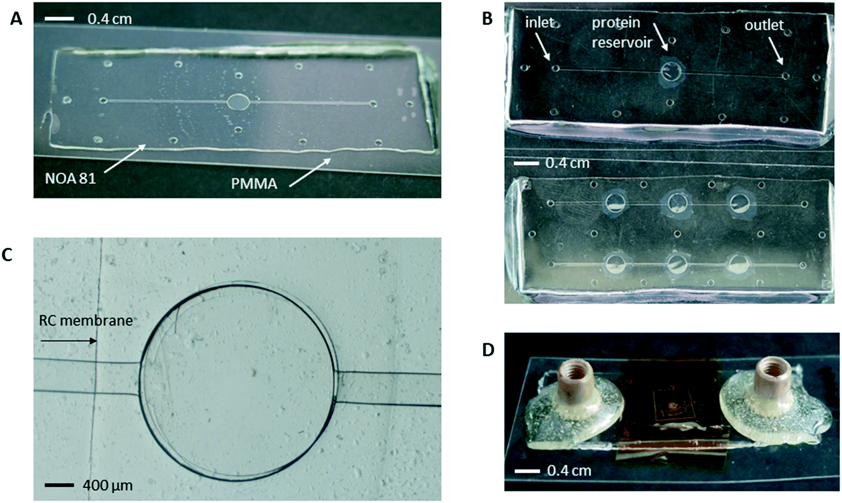 | ||
| Fig. 2 NOA 81 microfluidic chips embedding an RC dialysis membrane for the on-chip crystallization of proteins and in situ X-ray measurements. (A) NOA 81 microchip on a 175 μm thick PMMA substrate. Volume of protein reservoir: 0.7 μL. (B) Top view of the chip illustrated in (A) where the inlet/outlet for the fluidic connectors and the protein reservoir are shown (top). A microchip containing 6 protein reservoirs (0.7 μL each) for investigating phase diagrams via composition and temperature control (bottom). (C) Top view of the protein reservoir through an optical microscope. The RC dialysis membrane incorporated into the microchip can be distinguished. (D) Picture of a microchip ready-to-use for the on-chip crystallization of proteins. The protein sample is encapsulated in the central reservoir by a piece of PMMA and Kapton tape. Peek Nanoport connectors are bonded on the inlet and outlet of the device with fast epoxy glue. | ||
As described so far, the reservoir dedicated to be used for the deposition of the protein sample remains open to the atmosphere. We used the following method to encapsulate the protein sample within the dialysis reservoir. Once the droplet of protein solution is deposited inside the reservoir right upon the dialysis membrane, silicone grease is placed around the protein reservoir and a small piece of PMMA is gently placed on the top. The contact between the NOA sticker and the PMMA piece is a solid/solid interface and the presence of the silicon grease between them doesn't ensure any kind of bonding or irreversible sealing. The only way to produce irreversible sealing would be to expose again the NOA resin to UV radiation while being in contact with the PMMA piece. However, this is not feasible considering that the NOA was completely polymerized after the second exposure during the fabrication of the microchips. In order to circumvent this limitation and to ensure a good sealing of the protein reservoir, a piece of Kapton tape is set above the PMMA layer in order to improve air tight closure of the reservoir, as shown in Fig. 2D. The Kapton tape is not in contact with the protein reservoir directly but with the PMMA piece that is first set above the reservoir. The PMMA piece ensures that no contamination of the protein sample can occur and the Kapton tape will not fold or collapse into the reservoir. Another way to encapsulate the protein sample and seal the reservoir would be to directly set the Kapton tape right above the protein reservoir. However, this way of sealing would bring the sticky part of the Kapton tape in direct contact with the reservoir and would possibly have a negative influence on the crystallization process. The assembly also ensures the absence of leakages from the reservoir and the materials are bio compatible and show good transparency to X-rays for in situ measurements. The PMMA piece used for the encapsulation of the protein sample is the same as the sheet used as a substrate for the NOA stickers with a thickness of 175 μm. Moreover, the permeability of PMMA to gas is very low. PMMA has been characterized as impermeable to air.36 Peek NanoPort connectors were bonded on the inlet and outlet of the microfluidic channel using fast epoxy glue (Fig. 2D). Tubes plugged on these connectors were used to connect the microchip with the pressure driven system for fluid handling and mixing.
Once the protein is encapsulated within the dialysis reservoir, the filling of the chips is carried out by pushing the crystallization solutions into the microfluidic chip using the MFCS-EZ pressure system (Fluigent). The inlet pressure value varies depending on the solution used. Thus, for a solution with a viscosity close to that of water, the injection/inlet pressure varies between 20 and 60 mbar depending on the desired flow rate and between 50 and 150 mbar for more viscous solutions such as PEG (PEG 8000) at concentrations above 15% w/v. The solute diffusion across the membrane is imposed by a difference in concentration of the crystallizing agents (salt/PEG) between the two compartments of the microchip that are separated by the dialysis membrane. In our device, crystallization of the proteins occurs under static conditions regarding the protein solution and not under flowing conditions.40 This is a major asset as crystallizing the protein solutions under flowing conditions can be challenging and can affect the quality of the growing crystals.42,43 However, the crystallization solution can flow continuously within the microfluidic channel of our device, offering the possibility to exchange dynamically crystallization conditions while using the same protein sample, thus reducing also the consumption of the valuable protein sample.
The chips can be reused several times depending on the kind of crystallization solution used during the experiments. The Kapton tape and the PMMA piece can be easily removed from the protein reservoir. In the case of low viscosity solutions (salts), the chips can be reused several times if the dialysis membrane or the bonding of NOA on PMMA is not damaged. In the case of viscous solutions (PEG), it is better not to re-use the chip, unless the PEG solution can be removed from the channels using a water flow. Visual inspection of the dialysis membrane under a microscope after each experiment is the most direct way to observe any changes or damage to the membrane. Another way to observe changes in the membrane is by using water flow. If the membrane is damaged, the solution leaks through the protein reservoir and there is no effluent in the outlet point of the microchip. This way is more efficient to indirectly inspect the dialysis membrane because leakages occur every time, even when the membrane is not completely damaged. Both ways of inspecting the membrane are non-invasive and they don't alter the surface or the functionality of the membrane. The average lifetime of a microchip after its fabrication has been empirically estimated to be 6 months. After this time period, the chips become more fragile, especially regarding the NOA–PMMA adhesion.
SEM characterization of the microchips
Scanning electron microscopy (SEM) has been performed using a tabletop SEM microscope (TM3030, Hitachi). The SEM photographs (Fig. 3) zoom in the area where the RC dialysis membrane is embedded into the layer of the NOA resin. In Fig. 3A, a profile cross section of the microchip shows exactly the integration of the RC membrane into the layer of NOA. No traces of liquid NOA is observed to be absorbed on the membrane and this can be seen clearly in Fig. 3B. Fig. 3B is a SEM image taken after cutting the microchip near the central protein reservoir where the RC membrane is located. Specifically, in Fig. 3B we can observe a cross section of the area (after cutting the chip) where the dialysis membrane is indicated with a red arrow, the protein reservoir with a white arrow and the microfluidic channel with a green arrow. As may be seen, the membrane is not chemically bonded to the resin. Despite this fact, no leakages were observed across the membrane and between the dialysis reservoir and the fluidic channel, for our operating pressure range (20–60 mbar for aqueous solutions or 50–150 mbar for more viscous solutions) during the crystallization experiments.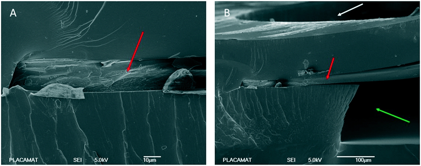 | ||
| Fig. 3 SEM images obtained from a profile cross section of the chip. (A) The dialysis membrane integrated into the NOA resin and (B) a view highlighting the protein reservoir (white arrow) and the microfluidic channel (green arrow). The red arrows in both cases indicate the RC dialysis membrane. | ||
Crystallization experiments
Chicken egg-white lysozyme was purchased from Sigma Aldrich as a lyophilized powder, dissolved in distilled water and filtered to obtain a solution with a final concentration of ∼30 mg mL−1. Insulin from porcine pancreas was also purchased from Sigma Aldrich as a lyophilized powder, dissolved in 0.5 M hydrochloric acid at pH 3 and filtered to obtain a solution with a final concentration of ∼2.5 mg mL−1. IspE, a kinase from Agrobacterium tumefaciens, was used with a final concentration of ∼10 mg mL−1 (F. Borel et al.48). All protein solutions were filtered through 0.22 μm Millipore filters prior to their use. The membranes integrated into the chip were the standard regenerated cellulose (RC) membranes Spectra/Por® (Spectrum Labs). The crystallization mixtures were all centrifuged and filtered to remove all solid particles (precipitate, dust or nuclei of crystals) prior to their use. Table 1 summarizes the experimental conditions (protein concentration, initial concentration of the crystallization solution, MWCO of the membrane, and temperature) for the on-chip crystallization of lysozyme, IspE and insulin through the dialysis method.| Protein | Protein concentration (mg mL−1) | Initial concentration of reservoir solution | Membrane MWCO (kDa) | Temperature (K) |
|---|---|---|---|---|
| Lysozyme | ∼30 | 0.75–0.85 M NaCl | 6–8 | 293–300 |
| 100 mM CH3COONa pH 4 | ||||
| IspE | ∼10 | 18% (w/v) PEG 8000 | 12–14 | 293 |
| 5 mM MgCl2 | ||||
| 5 mM ATP | ||||
| 100 mM Na3C6H5O7 pH 6 | ||||
| Insulin | ∼2.5 | 1 mM HCl | 3.5 | 293 |
| 5 mM ZnCl2 | ||||
| 50 mM Na3C6H5O7 pH 6 | ||||
| 10% (v/v) C3H6O |
Results and discussion
Crystallization experiments
The crystallization tests were carried out using three different proteins. These proteins have various molecular weights and diverse conditions to crystallize which enables the investigation of the versatility of the microfluidic chip. For example, we tested the resistance of the microchip against the different chemicals used during the crystallization experiments like sodium chloride (NaCl), sodium acetate (CH3COONa), sodium citrate (Na3C6H5O7), polyethylene glycol (PEG) of molecular weight from 1 to 8 kDa, acetone (C3H6O) and hydrochloric acid (HCl) or additives like magnesium chloride (MgCl2), zinc chloride (ZnCl2) or adenosine triphosphate (ATP).Chicken egg-white lysozyme
In this section, we describe the crystallization of lysozyme on the microchips in order to demonstrate the control over the crystallization process and verify the reversibility of the dialysis method by modifying the temperature or the concentration of the precipitant solution. The experimental conditions are summarized in Table 1. Temperature and concentration gradients were used to nucleate, grow and dissolve the crystals. Fig. 4 (top) shows the nucleation and growth of lysozyme crystals (a), the dissolution of the crystals using temperature (b), their re-nucleation (c) and finally their re-dissolution using concentration as a variable (d). The respective phase diagrams showing the kinetic pathway for each case are illustrated in Fig. 4 (bottom). The red arrows show the kinetic trajectory of the dialysis method for crystallization. During the onset of the experiment, the temperature was set at 293 K. Nucleation occurred and lysozyme crystals grew within the protein reservoir, as shown in Fig. 4a. Then, the temperature was increased gradually up to 300 K, while the concentration of the crystallization solution remained constant, in order to dissolve the crystals (Fig. 4b top). This step is consistent with the fact that lysozyme has a direct solubility, i.e. the solubility increases with temperature rise. After total dissolution of the crystals, the temperature was then rapidly decreased to the initial temperature value (293 K) and new, smaller crystals nucleated and subsequently grew (Fig. 4c). This second nucleation event appeared faster than the first one (Fig. 4a), as the protein reservoir was already at equilibrium with respect to the precipitant concentration. The last step of the experiment (Fig. 4d) was to exchange the crystallization solution circulating within the microfluidic channels with buffer solution (without salt), in order to dissolve the newly formed crystals. The second dissolution occurred due to the concentration gradient between the protein reservoir and the buffer solution, while the temperature remained constant at 293 K. The first dissolution event achieved through temperature control was completed within 15 min and the second one, achieved through control over the precipitant concentration, was completed after 60 min. This observation is not peculiar, since equilibrium concentration needs to be reached inside the protein reservoir before dissolution occurs.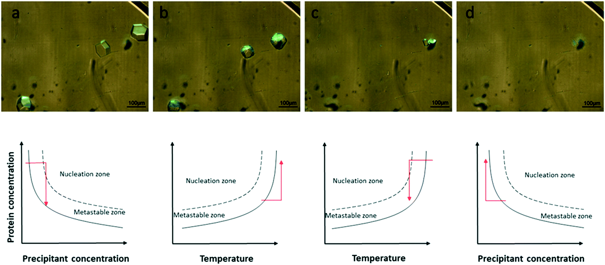 | ||
| Fig. 4 Crystallization and dissolution experiment performed on-chip via the micro-dialysis method using ∼30 mg mL−1 lysozyme. a) Nucleation and growth at 293 K, NaCl 0.75 M. b) Dissolution at 300 K, NaCl 0.75 M. c) Fast nucleation at 293 K, NaCl 0.75 M. d) Dissolution at 293 K, NaCl 0 M. The top figures show crystals of lysozyme grown inside the protein reservoir of the microfluidic chip for conditions a–d. The bottom figures are a schematic view of the respective phase diagrams as a function of the precipitant concentration (a and d) when the temperature is constant or as a function of temperature (b and c) when the precipitant concentration is constant. The red arrows illustrate the kinetic trajectory for the dialysis crystallization experiments. | ||
In Fig. 4a tetragonal lysozyme crystals can be seen. Crystals with the same morphology were also observed by Hansen et al.22 who used free interface diffusion (FID) in a microfluidic device. This crystallization method promoted the formation of large single lysozyme crystals. However, in the rest of the photos in Fig. 4 this typical morphology is changing since the lysozyme crystals undergo temperature- or concentration-based variations. Variations in the morphology of lysozyme crystals were also reported by Talreja et al.17 who developed an evaporation-based crystallization platform. In this device crystallization occurs through evaporation: protein and precipitant solutions are mixed in a droplet which gradually gets concentrated through evaporation of the solvent.
IspE from Agrobacterium tumefaciens
A crystallization experiment of IspE from Agrobacterium tumefaciens was conducted to demonstrate the compatibility of the microfluidic chips for experiments with long duration. The experimental conditions are summarized in Table 1. Fig. 5 shows the nucleation and growth of IspE crystals at different time intervals from the onset of the experiment. Specifically, IspE crystals are shown after 6 days from the beginning of the experiment (Fig. 5a), after 19 days (Fig. 5b) and after 50 days (Fig. 5c). The MWCO of the dialysis membrane used for this experiment was sufficient to allow the diffusion of PEG through the membrane and protein retention. During this experiment, the crystallization solution flows continuously within the microfluidic channel with a pressure of approximately 90 mbar. In order to ensure continuous flow within the microfluidic channel, the external reservoir containing the crystallization solution was refilled when it was necessary.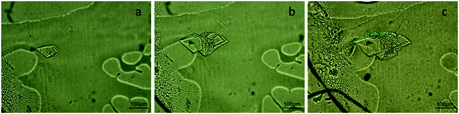 | ||
| Fig. 5 Crystals of IspE (∼10 mg mL−1) grown on-chip via the micro-dialysis method after a) 6 days, b) 19 days and c) 50 days from the onset of the experiment. Crystallization conditions: 8% w/v PEG 8000, 5 mM MgCl2, 5 mM ATP, 0.1 M sodium citrate pH 6 and T = 293 K. | ||
For experiments with long duration, dynamically monitoring the on-chip protein crystallization via the dialysis method would provide further information on the kinetics of the process and we are currently working towards this direction. For the experiments conducted in the present work, only photos of the crystallization process in specific time intervals were taken with the aid of a digital camera connected to a microscope.
IspE and insulin for serial X-ray data collection
The dialysis method allows the growth of numerous, isomorphous micro crystals required to perform serial X-ray diffraction experiments. A large number of micro crystals of IspE (Fig. 6a) and insulin (Fig. 6b) were grown. The conditions of the experiments are given in Table 1. In the microdialysis experiment in the case of IspE, the crystallization solution circulated in the microfluidic channel (Table 1) was balanced against the solution of the mixture of the protein (∼10 mg mL−1 in 50 mM Hepes pH 7, 3 mM DTT, 0.1 M NaCl, 1 mM MgCl2) with ATP (5 mM) in Na3C6H5O7 buffer pH 6, housed in the dialysis reservoir of the microchip. The main difference between the crystallization experiments illustrated in Fig. 5 and 6a is the final supersaturation obtained in the dialysis chamber (i.e. the concentration of PEG 8000). Therefore, compared to Fig. 5, which shows the low symmetry monoclinic IspE crystal in the presence of 8% PEG 8000, at 18% PEG 8000 (Fig. 6a), the number of these crystals is much larger while their size is much smaller.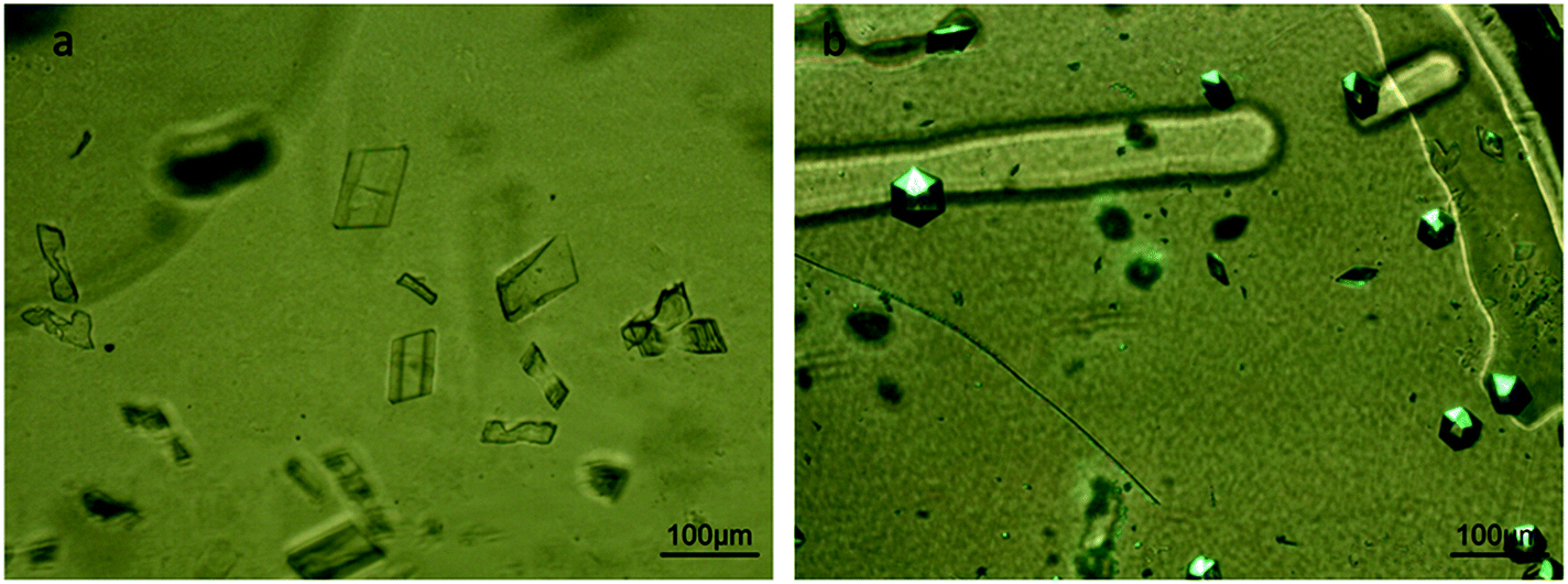 | ||
| Fig. 6 Multiple isomorphous single a) IspE and b) insulin crystals grown on-chip via the micro-dialysis method, used for collecting in situ X-ray diffraction data. Crystallization conditions: for IspE 18% w/v PEG 8000, 5 mM MgCl2, 5 mM ATP, and 0.1 M Na3C6H5O7 pH 6 and for insulin: 1 mM HCl, 5 mM ZnCl2, 50 mM Na3C6H5O7 pH 6 and 10% v/v acetone. Crystals of both proteins were grown at 293 K. | ||
For the crystallization of IspE, ATP is one of the molecules comprising the solution of the protein reservoir. Due to its molecular weight, ATP can diffuse across the dialysis membrane, thus lowering the ATP concentration in the protein reservoir and modifying crystallization conditions. Therefore, it is mandatory that ATP is also present in the composition of the crystallizing agent and has to be used as a co-factor in the crystallization process. In this case, it is better to inject the crystallizing agent sequentially instead of preserving continuous flow within the channel of the microfluidic chip. For the experiments carried out with insulin, the chosen crystallization conditions contained up to 10% v/v acetone. These conditions were first tested to grow insulin crystals by the vapor diffusion method (hanging drop). Insulin crystals were grown under the same conditions within the chip, despite the use of highly volatile acetone in the synthesis of the crystallization solution. Acetone proved to be compatible with the materials of the microfluidic device and the RC dialysis membrane. In Fig. 6b, rhombohedral insulin crystals were grown at 293 K via dialysis. There are many examples in the literature where insulin crystals are grown in various crystallization experiments and using various techniques. For example, Kwon and Kim45 grew insulin crystals using the seeding method, and Parambil et al.46 used flow in capillarities to enhance the nucleation of insulin crystals, while Borgstahl et al.47 grew large well-ordered insulin crystals in microgravity. However, the morphology of the crystals also depends on the crystallization method. Dialysis offers a different kinetic pathway compared to other crystallization methods.
Material characterization for in situ X-ray diffraction
When microfluidic devices are used for on-chip in situ X-ray diffraction experiments, the contribution of the interactions between the materials composing the chip and the X-rays must be considered. The diffraction signal from the crystals is added to the signal known as background noise. Background noise is generated by the diffusion of X-rays through the materials used to manufacture the chip and any other materials that interfere between the chip and the detector, as for example the air. This signal-to-noise ratio between the diffraction signal coming from the crystals and the background noise generated by attenuation or scattering of X-rays through matter should be maintained as high as possible during data collection. Thus, it is crucial to characterize the materials used for fabricating the microfluidic devices in order to minimize phenomena that degrade the signal-to-noise ratio of the diffracted crystals.14 The materials of such a device should generate a minimum background signal, while being biocompatible and compatible with mechanical constraints imposed by the application.Diffraction data of lysozyme, IspE and insulin crystals grown on-chip with the microdialysis method were collected at the BM30A-FIP beamline at the European Synchrotron Radiation Facility (ESRF) using an X-ray wavelength of 0.98 Å. The beamline is equipped with an ADSC Quantum 315r detector with a matrix of 3 × 3 CCD for an active surface of 315 × 315 mm and resolution of 9.4 mega pixels. The microchips were mounted in front of the X-ray beam using the robotic arm G-Rob and a sample support that we designed for these experiments (Fig. ESI 4†).
Before the data collection of protein crystals, the microchips were characterized in the same facility. The microchips were placed on the support, mounted on the beamline and exposed to the same wavelength (0.98 Å). In order to perform on-chip X-ray diffraction experiments, it is essential to select appropriate materials for the microchips.14 Thus, prior to data collection from protein crystals, the scattering background of the microfluidic chip that we developed was compared to the background noise generated by two conventional plates for crystallization screening and in situ X-ray diffraction, Greiner CrystalQuickX and Crystal Cube by Cube Biotech. The part of the microfluidic device that is exposed to the X-ray beam is only the protein reservoir composed of the Kapton tape (∼20 μm thickness), the PMMA piece below the Kapton tape and the PMMA substrate of the microchip (350 μm thickness both) and the RC dialysis membrane (∼40 μm thickness). The distance between the chip/commercial plate and the detector was 200 mm. Fig. 7a illustrates the intensity versus resolution graphs for the microchip and the two commercial plates. The intensity corresponds to the value recorded by the detector for each device, after subtracting the measurement done without any sample (chip or plate) in front of the beam, i.e. subtracting the measurement for the atmosphere surrounding the materials, which in this case is helium. It is obvious that our device generates less background noise compared to the other two crystallization plates, as indicated by the broad peak in Fig. 7a. Reducing the thickness of the device is crucial for in situ data collection.3,14 Low thickness translates to less matter interference in the path of the X-ray beam. The protein reservoir of the microfluidic chip that we designed has a total thickness of ∼410 μm which is affected by the interaction with X-rays because the layer of NOA is out of the X-ray beam path, while the respective thickness for the CrystalQuickX plate is ∼700 μm. However, a very low thickness can lead to excessive evaporation and issues associated with the rigidity of the microchip itself.8 Our microchip proposes a fair compromise between the rigidity of the device and the reduction of background noise for data collection.
 | ||
| Fig. 7 a) Background scattering intensity as a function of resolution (Å) for the microfluidic chip developed in the present work and conventional crystallization plates (CrystalQuickX and CrystalCube). b) Background scattering intensity as a function of resolution (Å) from the materials composing the microfluidic assembly (2 × 175 μm thick PMMA sheet, ∼20 μm thick Kapton tape and ∼40 μm thick RC dialysis membrane). | ||
Apart from the thickness of the microfluidic assembly, the scattering signal of each material composing the device was also measured. Using low density materials to fabricate the chip is as important as reducing the thickness, because high molecular weight materials add up matter across the way of the X-ray beam resulting in increased background noise. The materials investigated were the Kapton tape, the RC dialysis membrane and the PMMA sheet. Each material was exposed for 20 s to the X-rays (wavelength 0.98 Å) and each measurement was followed by an exposure of 20 s to the surrounding environment. For example, the exposure of the PMMA sheet was followed by an exposure to an empty space, where no material apart from air interfered between the beam and the detector, and so on. However, instead of air we used helium flux, as it is lighter than air and contributes less to scattering effects. The amplitude of X-ray scattering increases with the atomic number of each element. The distance between the sample and the detector was 200 mm. Scattering images were viewed using Adxv and radial intensity plots were designed using ROOT. In Fig. 7b, the intensity of background scattering of various materials is plotted against resolution (Å). For PMMA, a wide peak is present between 4 and 8 Å and then the intensity decreases. The broad peak corresponds to the diffusion of X-rays in the material. In the case of Kapton tape, the peak is even more diffuse. On the other hand, even if the contribution of the RC dialysis membrane to the total background noise is very small, a peak can be observed between 4 and 5 Å. The noise generated from the microchip is maximum (peak) at low resolution (6–7 Å), which is less critical for processing the data at higher resolution. Moreover, the background noise obtained from the microchip is still 15 to 27 times lower than the background noise of commercial crystallization plates (Fig. 7a). The intensity in all the curves corresponds to the value recorded by the detector for each material, after subtracting the measurement done without any sample in a helium atmosphere. Helium flux can also be used while collecting diffraction data from protein crystals. This way, the surrounding environment during X-ray diffraction measurements and the one during the experiments conducted for the characterization of the chip's materials are the same and can be used as reference and be subtracted from each measurement.
In situ X-ray diffraction measurements from protein crystals
In situ X-ray diffraction data from lysozyme, IspE and insulin crystals grown on-chip were collected at the BM30A-FIP beamline (ESRF). The wavelength of the X-ray beam was 0.98 Å and the exposure times and the oscillation angles used for all the crystals were comparable. The data collection was carried out at room temperature. The microchips containing the protein crystals were mounted on the beamline using the 3D printed support described in Fig. ESI 4.† Reflections were processed, indexed and integrated using XDS.37 Molecular replacement and refinement were performed using the CCP4 suite.38Diffraction data sets were collected from single crystals grown within the protein reservoir of the chip and data were eventually merged. Statistics for different crystals of lysozyme, IspE and insulin, as well as merged data, are shown in Table 2. The composition of the crystallization solutions is given in Table 1. However, for the in situ X-ray diffraction experiments, lysozyme crystals were grown in 0.85 M NaCl (2nd column, Table 2) or 0.75 M NaCl (3rd column, Table 2) and IspE was crystallized in 20% w/v PEG 8000 (4th and 5th column, Table 2). The mosaicity of the crystals grown on-chip and analyzed in situ by X-ray diffraction at room temperature is significantly lower compared to the respective value obtained from crystals of the same protein crystallized using another experimental set up and analyzed by X-rays at cryogenic temperature.9 Specifically, for lysozyme crystals grown on-chip in a crystallization solution with 0.75 M NaCl, the measured mosaicity at room temperature was 0.07° (Table 2). On the other hand, the observed mosaicity at cryogenic temperature of lysozyme crystals grown with the conventional vapor diffusion (hanging drop) method under the same crystallization conditions was much higher, 0.328°, and the respective value for crystals grown with the previously described dialysis method was 0.128°.9 It is noteworthy that the compared values of the mosaicity were obtained via XDS statistics, on the same ESRF beamline, with the beam of photons of equivalent intensity and on crystals comparable in size. Therefore, such an observation can be attributed to the slowly varying conditions required for early crystal nucleation and relatively undisturbed lattice formation of crystals that we are able to achieve in the chip as well as the further absence of handling the crystals. This observation is in agreement with similar results reported elsewhere.13 In addition, recently it has been demonstrated that specific and global radiation damage are much less decoupled at room temperature than they are at cryogenic temperatures.39 These observations illustrate the interest in reviving the practice of collecting X-ray diffraction data of biological macromolecules at room temperature at synchrotron sources.
| Protein | Lysozyme (1 crystal) | Lysozyme (1 crystal) | IspE (1 crystal) | IspE (6 crystals) | Insulin (1 crystal) | Insulin (6 crystals) |
|---|---|---|---|---|---|---|
| Resolution (Å) | 50–1.60 (1.70–1.60) | 50–1.45 (1.54–1.45) | 50–2.15 (2.28–2.15) | 50–2.30 (2.40–2.30) | 50–2.00 (2.12–2.00) | 40–2.10 (2.20–2.10) |
| Mosaicity (°) | 0.06 | 0.07 | 0.11 | 0.18 | ||
| Space group | P43212 | P43212 | C2 | C2 | R3 | R3 |
| Unit cell parameters | 79.23, 79.23, 37.90 | 79.27, 79.27, 37.94 | 72.48, 82.91, 51.01 | 72.73, 82.92, 51.17 | 82.58, 82.58, 34.11 | 82.58, 82.58, 34.12 |
| 90, 90, 90 | 90, 90, 90 | 90, 109.08, 90 | 90, 109.20, 90 | 90, 90, 120 | 90, 90, 120 | |
| Total reflections (observed) | 50351 |
65652 |
19362 |
91062 |
7353 | 34986 |
| Unique reflections (observed) | 14911 |
12725 |
9716 | 22461 |
4194 | 9612 |
| Redundancy | 3.38 (3.13) | 5.16 (3.83) | 1.99 (1.91) | 4.05 (2.88) | 1.75 (1.66) | 3.64 (2.77) |
| Completeness (%) | 90.5 (93.4) | 57.8 (63.0) | 62.1 (64.8) | 89.5 (74.0) | 71.5 (74.7) | 94.9 (91.1) |
| I/σ | 13.1 (2.9) | 15.3 (2.3) | 8.0 (2.0) | 5.8 (1.9) | 6.8 (2.0) | 7.0 (2.7) |
In the case of lysozyme (Table 2), complete data sets have been obtained from single crystals. Indeed, due to the high symmetry of lysozyme crystals, there was no need to use X-ray serial crystallography in order to collect data sets from various crystals and then merge these data. Despite the fact that the data collection was carried out at room temperature, no damage of the crystals was observed. In contrast, IspE symmetry and accessible angle amplitude did not allow the collection of a complete data set from one crystal. The statistics for a merged data set obtained combining the data sets from six isomorphous IspE crystals randomly oriented with various crystals qualities are shown in Table 2 (5th column). In the case of insulin, the partial data sets of six isomorphous crystals were merged in order to provide a complete data set (Table 2, 7th column). However, insulin crystals were much smaller than IspE crystals (<50 μm). Despite the presence of microcrystals, it was feasible to collect data in situ using the microfluidic device that we developed.
Electron density maps
Electron density maps from insulin and IspE (Fig. 8 a and b) have been obtained at 2.1 Å and 2.3 Å resolution, respectively. Structure refinement worked correctly as indicated by R-work factors of 0.15 and 0.16 and R-free factors of 0.20 and 0.21, respectively for insulin and IspE. The derived electron density maps, generated from the merging of various data sets obtained through in situ X-ray diffraction for both proteins, illustrate the quality of detailed structural information that can be achieved. In addition, our diffraction analyses demonstrate the compatibility of our microfluidic chips with serial X-ray crystallography.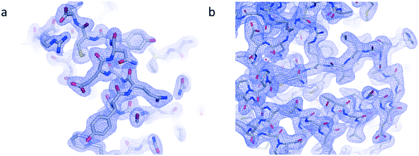 | ||
| Fig. 8 Electron density maps derived from crystallographic data collected from multiple crystals of a) insulin and b) IspE. The maps at 2.1 Å and 2.3 Å resolution, respectively, are contoured at 1σ. | ||
Conclusions
A microfluidic chip has been developed for on-chip protein crystallization using the micro-dialysis method. The device was designed in order to integrate commercially available RC dialysis membranes within the chip in a reproducible way for on-chip protein crystallization. The MWCO range of the RC membranes can vary from 3.5 to 14 kDa depending on the protein sample and the crystallization conditions. The flexibility of choosing the MWCO of the membrane, the rapid prototyping of the microfluidic chips and the relatively low cost of the materials enable the fabrication of numerous chips. The protocol presented in this work can be upgraded in order to fabricate microchips with different types and MWCOs of the embedded membranes.Once protein crystals were grown on-chip, in situ X-ray diffraction data were collected for all three proteins investigated in this work. Complete data sets were collected at room temperature from single crystals of lysozyme, whereas diffraction data from six isomorphous microcrystals of IspE and insulin were merged to yield complete data sets, demonstrating the compatibility of our microfluidic device with serial X-ray crystallography experiments. In situ data collection was rendered feasible due to the relatively high X-ray transparency of the materials chosen to produce the microchips and the low background noise of the microfluidic assembly. Indeed, diffraction data were collected from the materials composing the microfluidic chip in order to evaluate the background noise generated by the scattering and attenuation of X-rays. The low level of background scattering of the microchip, especially at high resolution values required for structure determination in protein crystallography, is evidence that high quality diffraction data can be collected. Moreover, this chip allows the in situ collection of X-ray diffraction data at room temperature, avoiding problems encountered with conventional cryoprotectants. The automation level of the whole process is enhanced by the use of a 3D printed support, adapted to mount up to 3 chips simultaneously in front of the beam at automated in situ X-ray diffraction beamlines. Therefore, there is no need to harvest crystals from the crystallization setup and transfer them to the beam, steps that can add up stress to the fragile protein crystals. We have developed a microfluidic chip that includes all the stages in the crystallization pipeline, from crystal growth using micro-dialysis to in situ data collection and does not require any handling of the protein crystals prior the X-ray diffraction experiment. In addition to using relatively inexpensive materials for fabrication, the chips can be reused several times as long as they are sufficiently washed, they don't show any mechanical damage and the dialysis membrane is not detached from the NOA sticker.
Our microchips can be used also for screening and optimizing crystallization conditions for mapping temperature–precipitant concentration phase diagrams. A large number of isomorphous crystals suitable for serial X-ray crystallography can be grown on-chip through reversible control over the concentration and temperature conditions, using a low volume (0.2–0.7 μL) of the protein sample. The combination of precise and dynamic chemical composition control, a prototype for temperature control, real time observation and in situ X-ray diffraction studies is promising for new, challenging areas of investigation such as the crystallization of membrane proteins. We expect that this inexpensive device would contribute significantly to the field of structural biology through serial X-ray crystallography studies at synchrotron and XFEL sources.
Conflicts of interest
There are no conflicts to declare.Acknowledgements
MBS thanks the CEA's International Doctoral Research Program (Irtelis) for the PhD Fellowship to NJ, and SJ acknowledges the Horizon 2020 Research and Innovation Program of the European Union under grant no. 722687 for the fellowship MARIE SKŁODOWSKA – CURIE. MBS acknowledges the support of the MI/CNRS under the contract Instrumentation at the limits 2014–2015. The authors extend their special thanks to Dr Jean-Luc Ferrer (Synchrotron Group, IBS, Grenoble), who took active interest in taking forward the protein crystallization problem for protein crystallography. JBS acknowledges CNRS and Solvay for funding. MBS, NJ and SJ thank LIPhy for the clean room to perform microfabrication. IBS acknowledges integration into the Interdisciplinary Research Institute of Grenoble (IRIG, CEA).References
- J. M. Martin-Garcia, C. E. Conrad, J. Coe, S. Roy-Chowdhury and P. Fromme, Arch. Biochem. Biophys., 2016, 602, 32–47 CrossRef CAS PubMed.
- R. L. Owen, D. Axford, D. A. Sherrell, A. Kuo, O. P. Ernst, E. C. Schulz, R. J. Dwayne Miller and H. M. Mueller-Werkmeister, Acta Crystallogr., Sect. D: Struct. Biol., 2017, 73, 373–378 CrossRef CAS PubMed.
- Y. Gicquel, R. Schubert, S. Kapis, G. Bourenkov, T. Schneider, M. Perbandt, C. Betzel, H. N. Chapman and M. Heymann, J. Visualized Exp., 2018, 134, e57133 Search PubMed.
- H. N. Chapman, et al. , Nature, 2011, 470, 73–78 CrossRef CAS PubMed.
- S. Sui and S. L. Perry, Struct. Dyn., 2017, 4, 032202 CrossRef.
- S. Guha, S. L. Perry, A. S. Pawate and P. J. A. Kenis, Sens. Actuators, B, 2012, 174, 1–9 CrossRef CAS PubMed.
- V. Miralles, A. Huerre, F. Malloggi and M.-C. Jullien, Diagnostics, 2013, 3, 33–67 CrossRef PubMed.
- S. Sui, Y. Wang, K. W. Kolewe, V. Srajer, R. Henning, J. D. Schiffman, C. Dimitrakopoulos and S. L. Perry, Lab Chip, 2016, 16, 3082–3096 RSC.
- N. Junius, E. Oksanen, M. Terrien, C. Berzin, J.-L. Ferrer and M. Budayova-Spano, J. Appl. Crystallogr., 2016, 49, 806–813 CrossRef CAS PubMed.
- Š. Selimović, F. Gobeaux and S. Fraden, Lab Chip, 2010, 10, 1696–1699 RSC.
- P. Laval, C. Giroux, J. Leng and J.-B. Salmon, J. Cryst. Growth, 2008, 310, 3121–3124 CrossRef CAS.
- J. Leng and J.-B. Salmon, Lab Chip, 2009, 9, 24–34 RSC.
- S. L. Perry, S. Guha, A. S. Pawate, A. Bhaskarla, V. Agarwal, S. K. Nair and P. J. A. Kenis, Lab Chip, 2013, 13, 3183–3187 RSC.
- K. Dhouib, et al. , Lab Chip, 2009, 9, 1412–1421 RSC.
- C. L. Hansen, E. Skordalakes, J. M. Berger and S. R. Quake, Proc. Natl. Acad. Sci. U. S. A., 2002, 99, 16531–16536 CrossRef CAS PubMed.
- B. Zheng, L. S. Roach and R. F. Ismagilov, J. Am. Chem. Soc., 2003, 125, 11170–11171 CrossRef CAS.
- S. Talreja, D. Y. Kim, A. Y. Mirarefi, C. F. Zukoski and P. J. A. Kenis, J. Appl. Crystallogr., 2005, 38, 988–995 CrossRef CAS.
- L. Li, D. Mustafi, Q. Fu, V. Tereshko, D. L. Chen, J. D. Tice and R. F. Ismagilov, Proc. Natl. Acad. Sci. U. S. A., 2006, 103, 19243–19248 CrossRef CAS PubMed.
- W. Du, L. Li, K. P. Nichols and R. F. Ismagilov, Lab Chip, 2009, 9, 2286–2292 RSC.
- C. Sauter, K. Dhouib and B. Lorber, Cryst. Growth Des., 2007, 7, 2247–2250 CrossRef CAS.
- B. Zheng, J. D. Tice, L. S. Roach and R. F. Ismagilov, Angew. Chem., Int. Ed., 2004, 43, 2508–2511 CrossRef CAS PubMed.
- C. L. Hansen, S. Classen, J. M. Berger and S. R. Quake, J. Am. Chem. Soc., 2006, 128, 3142–3143 CrossRef CAS PubMed.
- G. Kisselman, W. Qiu, V. Romanov, C. M. Thompson, R. Lam, K. P. Battaile, E. F. Pai and N. Y. Chirgadze, Acta Crystallogr., Sect. D: Biol. Crystallogr., 2011, 67, 533–539 CrossRef CAS PubMed.
- J. M. Schieferstein, A. A. Pawate, M. J. Varel, S. Guha, I. Astrauskaite, R. B. Gennis and P. J. A. Kenis, Lab Chip, 2018, 18, 944–954 RSC.
- M. Heymann, A. Opthalage, J. L. Wierman, S. Akella, D. M. E. Szebenyi, S. M. Gruner and S. Fraden, IUCrJ, 2014, 1, 349–360 CrossRef CAS PubMed.
- M. Budayova-Spano, FR10/57354, UJF, 2010, (extension: EP117730945, US13821053, JP2013528746).
- M. Spano, J.-B. Salmon and N. Junius, FR3044685A1, UJF, 2015.
- J. Shim, G. Cristobal, D. R. Link, T. Thorsen and S. Fraden, Cryst. Growth Des., 2007, 7, 2192–2194 CrossRef CAS.
- J. de Jong, R. G. H. Lammertink and M. Wessling, Lab Chip, 2006, 6, 1125–1139 RSC.
- M. Kornreich, M. Heymann, S. Fraden and R. Beck, Lab Chip, 2014, 14, 3700–3704 RSC.
- L. Li and R. F. Ismagilov, Annu. Rev. Biophys., 2010, 39, 139–158 CrossRef CAS PubMed.
- Y. Li, J. Xuan, R. Hu, P. Zhang, X. Lou and Y. Yang, Talanta, 2019, 204, 569–575 CrossRef CAS PubMed.
- B. G. Abdallah, S. Roy-Chowdhury, R. Fromme, P. Fromme and A. Ros, Cryst. Growth Des., 2016, 16, 2074–2082 CrossRef CAS PubMed.
- D. Bartolo, G. Degré, P. Nghe and V. Studer, Lab Chip, 2008, 8, 274–279 RSC.
- M. Morel, J.-C. Galas, M. Dahan and V. Studer, Lab Chip, 2012, 12, 1340–1346 RSC.
- H. Y. Tan, W. K. Loke and N.-T. Nguyen, Sens. Actuators, B, 2010, 151, 133–139 CrossRef CAS.
- W. Kabsch, Acta Crystallogr., Sect. D: Biol. Crystallogr., 2010, 66, 125–132 CrossRef CAS PubMed.
- M. D. Winn, et al. , Acta Crystallogr., Sect. D: Biol. Crystallogr., 2011, 67, 235–242 CrossRef CAS PubMed.
- G. Gotthard, S. Aumonier, D. De Sanctis, G. Leonard, D. von Stetten and A. Royant, IUCrJ, 2019, 6, 665–680 CrossRef CAS PubMed.
- M. Skou, S. Skou, T. G. Jensen, B. Vestergaard and R. E. Gillilan, J. Appl. Crystallogr., 2014, 47, 1355–1366 CrossRef CAS PubMed.
- M. I. Vaquez, P. Galan, J. Casado, M. J. Ariza and J. Benavente, Appl. Surf. Sci., 2004, 238, 415–422 CrossRef CAS.
- P. G. Vekilov and F. Rosenberger, J. Cryst. Growth, 1998, 186, 251–261 CrossRef CAS.
- A. Kadowaki, I. Yoshizaki, L. Rong, H. Komatsu, O. Odawara and S. Yoda, J. Synchrotron Radiat., 2004, 11, 38–40 CrossRef CAS PubMed.
- A. A. S. Bhagat, P. Jothimuthu and I. Papautsky, Lab Chip, 2007, 7, 1192–1197 RSC.
- J.-H. Kwon and C.-W. Kim, J. Cryst. Growth, 2004, 263, 536–543 CrossRef CAS.
- J. V. Parambil, M. Schaepertoens, D. R. Williams and J. Y. Y. Heng, Cryst. Growth Des., 2011, 11, 4353–4359 CrossRef CAS.
- G. E. O. Borgstahl, A. Vahedi-Faridi, J. Lovelace, H. D. Bellamy and E. H. Snell, Acta Crystallogr., Sect. D: Biol. Crystallogr., 2001, 57, 1204–1207 CrossRef CAS PubMed.
- F. Borel, S. Richard, F. Pojer, L. Jacquamet, T. Baiga, J. A. Ramsey, A. Iannello, M. Bowman, J. P. Noel and J.-L. Ferrer, unpublished data.
Footnotes |
| † Electronic supplementary information (ESI) available. See DOI: 10.1039/c9lc00651f |
| ‡ Current address: ELVESYS – Innovation Center, 1 rue Robert et Sonia Delaunay, 75011 Paris, France. |
| This journal is © The Royal Society of Chemistry 2020 |