 Open Access Article
 This Open Access Article is licensed under a
 Creative Commons Attribution 3.0 Unported Licence
Introductory lecture: origins and applications of efficient visible photoluminescence from silicon-based nanostructures
Leigh
Canham

School of Physics and Astronomy, University of Birmingham, Edgbaston, Birmingham, B15 2TT, UK. E-mail: l.t.canham@bham.ac.uk
First published on 1st June 2020
Abstract
A variety of silicon-based nanostructures with dimensions in the 1–5 nm range now emit tunable photoluminescence (PL) spanning the visible range. Achievement of high photoluminescence quantum efficiency (PLQY) relies critically on their surface chemistry passivation and an impressive “tool box” of options have been developed. Two distinct PL bands are dominant. The “S-Band” (red–green emission with Slow microsecond decay) has PLQY that has steadily improved from ∼3% in 1990 to 65 ± 5% by 2017. The “F-Band” (blue–yellow with Fast nanosecond decay) has reported PLQY values that have improved from ∼0.1% in 1994 to as high as ∼90% by 2016. The vast literature on both bands is surveyed and for the S-band, size-structure-PL correlations and selective photo-excitation studies are highlighted. Resonant photoexcitation and single quantum dot studies have revealed the key role of quantum confinement and the excitonic phonon-assisted nature of the radiative transitions. For the F-band, in contrast, specific phenomenological studies are highlighted that demonstrate similar emission without the presence of silicon nanostructures. Low PLQY F-band emission from pure silicon–silica core shell systems is probably associated with oxide-related defects, but ultrahigh PLQY from many lower temperature synthesis routes is likely to be from carbon-based nanostructures or chromophores, not silicon nanostructures. Potential applications for both PL bands include sensing, medical imaging, theranostics, photovoltaics, LED colour converters and nano-thermometry. Emerging “green” synthesis routes are mentioned. If scalability and cost are significantly improved then a number of other proposed uses of ultra-efficient PL from “nano-Si” could become viable in cosmetics, catalysis, security and forensics.
1. Introduction
1.1. Scope of review
Nanostructuring has introduced an exciting new capability to semiconducting silicon: the ability to emit visible light very efficiently under photoexcitation (photoluminescence (PL)). This property was quickly recognized in the early 1990s as a route to extend the functionality of an already powerful silicon technology. The topic has thus received intense study over the last 30 years, with now thousands of publications. This review focuses on the visible photoluminescence of silicon nanostructures; collating both experimental and theoretical work on most types of nanostructure; providing quantitative performance metrics, particularly on photoluminescence quantum yield (PLQY); photoluminescence wavelength tunability (PLWT) and photoluminescence decay times (PLDT).There are two dominant PL emissions in the visible (see Fig. 1): the “Slow” (S) band in the red–yellow spectral range with long microsecond decay times (see Section 2) and the “Fast” (F) band in the blue–green with faster nanosecond decay times (see Section 3). In a given nanostructure, one or the other, or both can be present. Often, as shown in Fig. 1, the intensity of the blue emission will often increase with storage time. The origins of such behaviour have received intense study.
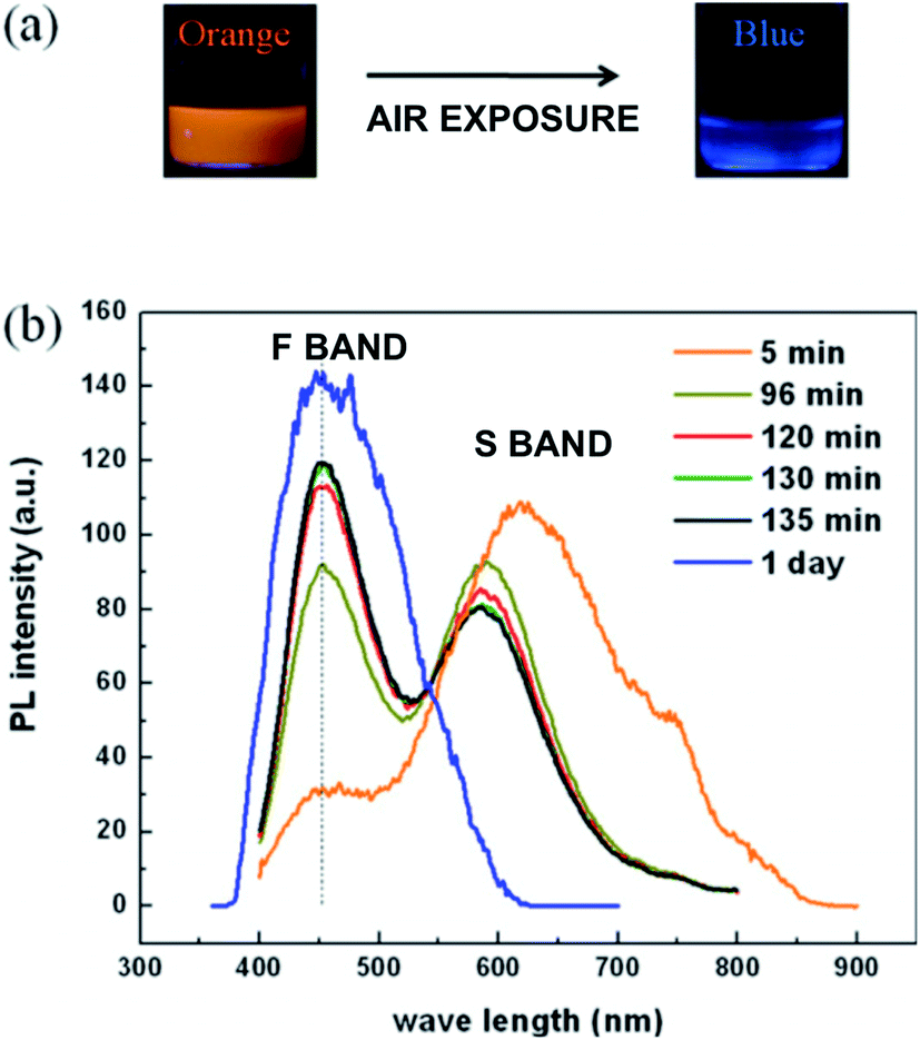 | ||
| Fig. 1 The S-band and F-band photoluminescence of silicon-based nanostructures.1 (a) Photographs of nanocrystal suspensions under UV illumination. Freshly etched nanocrystals: orange emission. After one day of air exposure: blue emission. (b) Evolution of S-band and F-band spectra with varying air exposure of the times indicated. Adapted with permission from A. Gupta and H. Wiggers, Nanotechnology, 2011, 22, 055707. Copyright IOP Publishing, 2011. All rights reserved. | ||
This review highlights many spectroscopy-based studies and selected phenomenological studies that provide insight into their likely PL mechanisms. The review also covers six application areas of efficient visible PL: sensing, photovoltaics, medical imaging, theranostics, white LEDs and nano-thermometry. It also proposes a number of ways in which the field might further progress, and other application areas that might emerge if cost and scalability issues are surmounted. There is no detailed discussion of nanostructure synthesis techniques and surface chemistry manipulation, as these have already been the focus of many prior reviews that are referenced.
Data on electrical transport, electroluminescence, optical gain, and thereby optoelectronics, are also omitted in order to entirely focus here on the potential of photoluminescent properties. Such a platform property is however often combined with other crucial ones for specific uses, such as biodegradability and biocompatibility for medical applications. These additional properties are covered briefly in the relevant application sections. In summary, this review collates and discusses some of the very large amount of data now available on many types of photoluminescent silicon nanostructures and many applications thereof. It is hoped to be of use both as a broad introduction to the vast literature of this maturing field, but should also stimulate specific areas of discussion and perhaps further research in highlighted topics.
1.2. Electron–hole recombination processes in bulk silicon
When a semiconductor such as silicon is stimulated by light (photoexcitation) it may return to equilibrium by a variety of processes.2 Some involve the re-emission of light (photoluminescence or fluorescence – these terms are used interchangeably in the literature on luminescent silicon nanostructures) and are so called radiative transitions. Others redistribute the absorbed energy amongst vibrational modes of the lattice or electronic excitations and ultimately generate heat – so-called non-radiative transitions.Radiative processes in silicon include recombination from electrons and holes3 free excitons,4 biexcitons or excitonic molecules,5–7 polyexcitons,8 electron–hole liquids,9,10 bound excitons11 and donor–acceptor pair luminescence.12–14 Free excitons will diffuse through the silicon lattice15 and can be trapped and emit light at isolated dopants,16 clusters of dopants,17 isoelectronic traps18 and sometimes near extended defects19–22 such as dislocations and precipitates. Such trapping can occur in the bulk and near surfaces. The majority of these radiative excitonic processes however are only observed at very low cryogenic temperatures, due to the small binding energy of the exciton. Not only that, but their efficiency is also normally low. The efficiency of a radiative process generally depends on the electronic bandstructure of the solid and for crystalline semiconductors the perfection of its lattice and surfaces, since most defects and surfaces promote non-radiative processes. Non-radiative processes23 in silicon are dominated by Auger recombination24 and recombination at “deep level” defects such as transition metal impurities in the bulk25 or defects at surfaces and interfaces such as that created by ambient or thermal oxidation of silicon.26
1.3. Photoluminescence of crystalline bulk silicon
It is instructive to first survey the PL of bulk Si because this reveals certain “spectroscopic fingerprints” of radiative excitonic recombination processes in this crystalline material. The fundamental indirect energy gap in crystalline bulk silicon, between the top of the valence band and lowest conduction band is 1.170 eV at 0 K, decreasing monotonically to 1.125 eV at 300 K.27 Interband near infrared photoluminescence from silicon was first observed by Haynes and co-workers in the 1950s.3 At room temperature its near bandgap emission consists of a single weak band at ∼1.09 eV (1134 nm) with a full width at half maximum (FWHM) that is about 100 meV.3,28,29 At cryogenic temperatures recombination becomes excitonic. The exciton in bulk silicon has a Bohr radius of 4.2 nm and a binding energy of only 14 meV.30Fig. 2 shows how the spectra broaden considerably above room temperature and sharpen considerably at cryogenic temperatures, with a spectral position that follows the temperature dependence of the silicon bandgap.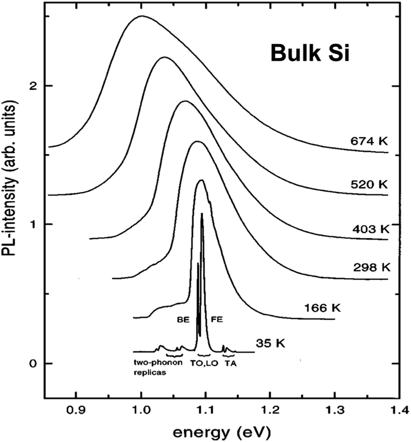 | ||
| Fig. 2 Normalized interband PL from bulk Si at 35–674 K.29 BE stands for bound exciton, FE for free exciton (see text). Reprinted with permission from V. Alex, S. Finkbeiner and J. Weber, J. Appl. Phys., 1996, 79, 6943. Copyright AIP Publishing. | ||
At low temperatures (<40 K) and in pure silicon, free exciton (FE) recombination totally dominates over bound exciton (BE) recombination (Fig. 3). Transition linewidths are now narrow enough to resolve fine structures corresponding to the TA and TO phonons as shown in Fig. 2 and 3. Two phonon replicas are very weak. Note the extremely weak “zero-phonon” peak I0 near 1.16 eV in Fig. 3 where electron and hole recombine without a momentum conserving phonon. The spacings of the features ITA and ITO from I0 in the spectrum are determined by the corresponding phonon energies. Currently accepted values for bulk silicon are: TA phonon = 18.4 ± 0.2 meV; LO phonon 56.2 ± 1 meV; TO phonon = 58.0 ± 1 meV. The relative ratios of the phonon-assisted peaks are temperature dependent but the TO mode is dominant with approximate values in Fig. 3 being 1 [TO]![[thin space (1/6-em)]](https://www.rsc.org/images/entities/char_2009.gif) :0.1 [LO]:0.03 [TA].31
:0.1 [LO]:0.03 [TA].31
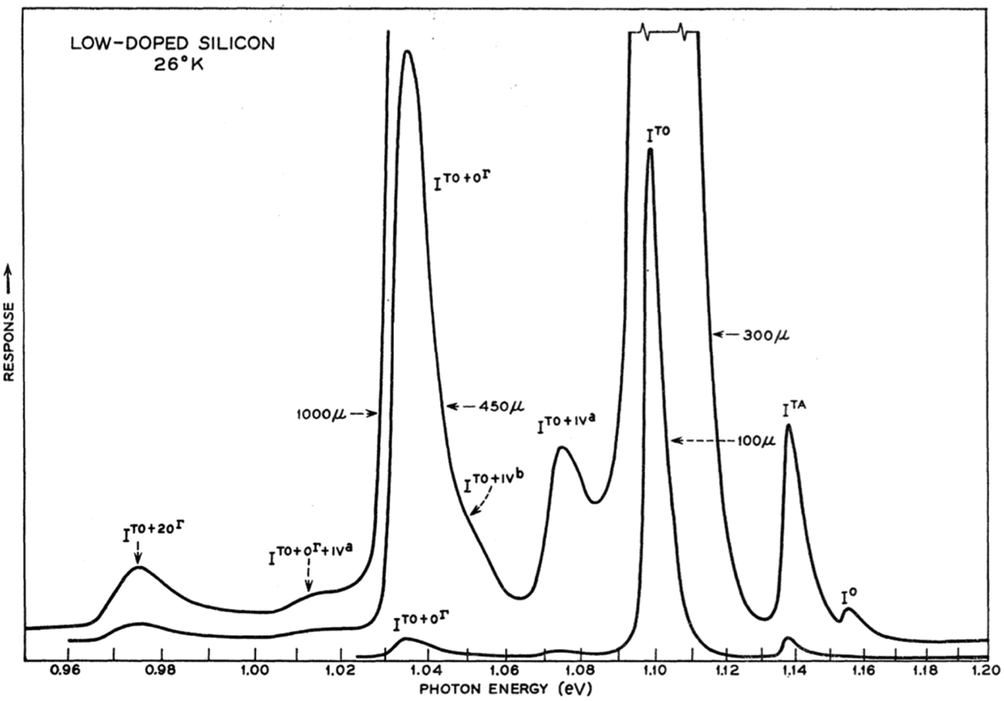 | ||
| Fig. 3 Intrinsic free exciton PL from high purity silicon at 26 K.16 The LO and TO phonon components are not resolved. Reprinted with permission from P. J. Dean, J. R. Haynes and W. F. Flood, Phys. Rev., 161, 711–729. Copyright the American Physical Society, 1967. | ||
Concerning defect-related emission let us first consider the simplest point defects: substitutional donors, like P, As and Sb; interstitial donors like Li; and substitutional acceptors like B, Al, Ga and In. Free excitons migrating through the lattice can bind to the neutral donor or acceptor and binding energies lie in the range 3–50 meV.31 When the exciton is localised on the impurity, there is a relaxation of the wave vector selection rule so the zero phonon line is thus much stronger for bound excitons (e.g. In0 in Fig. 4) than for free excitons (e.g. I0 in Fig. 3).
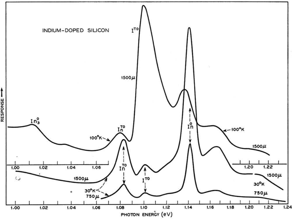 | ||
| Fig. 4 30–100 K PL due to bound exciton recombination at indium atoms.16 Reprinted with permission from P. J. Dean, J. R. Haynes and W. F. Flood, Phys. Rev., 161, 711–729, 1967. Copyright the American Physical Society, 1967. | ||
Rapid progress in identifying many radiative defects began in the late 1970s when Ge photodetectors became available and were orders of magnitude more sensitive than PbS detectors in the near infrared.31 The huge increase in resolution enabled isotope shifts in sharp zero phonon line transitions to be studied, thereby unambiguously identifying which impurities were involved in specific vibronic band emission. When combined with uniaxial stress measurements to elucidate the defect symmetry, and correlations with other spectroscopic techniques, detailed models of radiative point defects emerged.31
Unfortunately, some luminescent bulk silicon crystals also display broad featureless bands at sub-bandgap wavelengths19,21,32 providing a challenge for identification that researchers of today’s silicon nanostructures are more than well aware. Fig. 5 shows an example of a broad and featureless band at 0.94 eV attributed to extended defects (hydrogen platelets) in bulk silicon.21
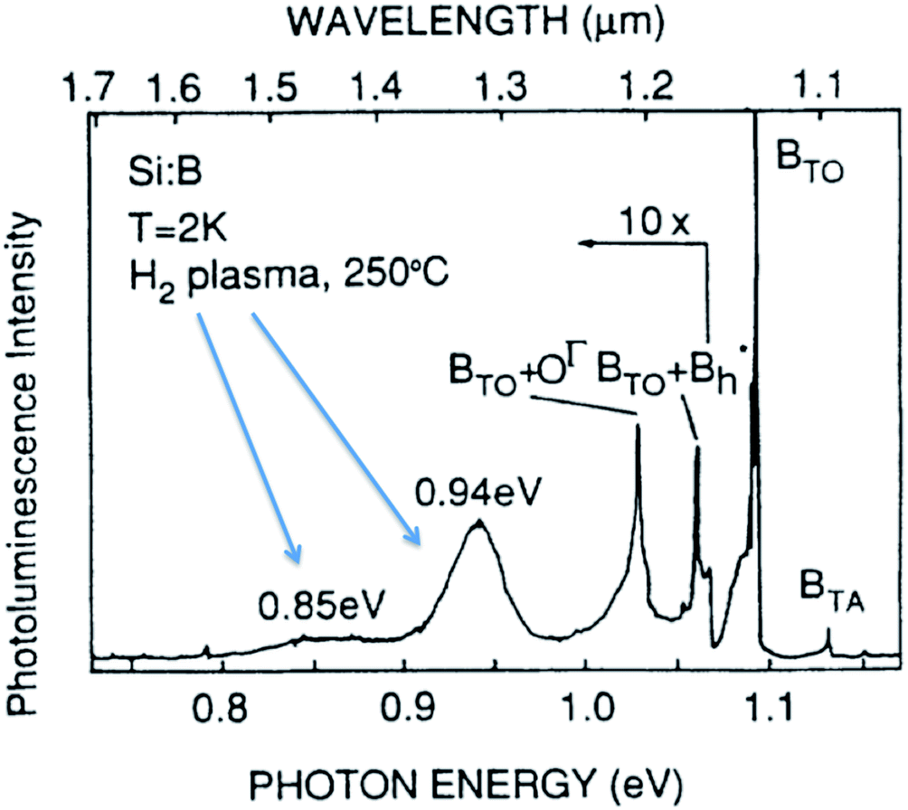 | ||
| Fig. 5 Low temperature PL from plasma etched bulk silicon with high levels of hydrogen.21 Reprinted and adapted with permission from H. Weman, B. Monemar, G. S. Oehrlein and S. J. Jeng, Phys. Rev. B, 42, 3109–3112, 1990. Copyright the American Physical Society, 1990. | ||
1.4. Surface passivation chemistries for bulk silicon
Surface or interface “passivation” refers to the removal of electrically or optically active defects and has become increasingly important in silicon solar cell technology due to the cost-driven reduction of cell thickness and corresponding increase in surface to volume ratio. There has been an associated significant effort in understanding the origin of, and minimizing, such non-radiative recombination. That literature is utilized here to identify some of the most useful passivation chemistries that could be applied to luminescent silicon nanostructures, and indeed many, but not all, have already been used. Given that nanostructures have huge surface areas, the importance of minimizing non-radiative surface recombination becomes of paramount importance if high PLQY is to be realized.Surfaces disrupt the band structure, creating energy states in the bandgap via strained or un-terminated (“dangling”) bonds. These states can capture electrons or holes with capture velocities Sn0 and Sp0 that are governed by the product of carrier diffusion, capture cross-section and defect density, Dit. A surface will have different steady-state carrier concentrations (ns, ps) of electrons and holes to those in the bulk, and different to the intrinsic carrier concentration (ni).
The total recombination at a surface can be characterized by an effective “surface recombination velocity (SRV)” that quantitatively assesses surface or interface passivation:
| Seff = (1/Δnd) × (nsps − ni2)/((ns + ni)/Sp0 + (ps + ni)/Sn0) | (1) |
| Si structure | Surface chemistry | Passivation method | SRV (cm s−1) | References |
|---|---|---|---|---|
| Bulk Si (111) | Silicon hydride | In situ in HF and other acids | <1 (0.25) | (Yablonovitch 1986)34 |
| Bulk Si | Silicon hydride | HF-based cleans | <0.05 → 0.1 | (Sun 2018)35 |
| Bulk Si (111) | Native oxide | HF and air exposure (24 days) | >1000 | (Nemanik 2006)36 |
| Bulk Si (100) | Thermal oxide | Annealed silica | <1 | (Kerr 2002)37 |
| Bulk Si | Thermal oxide | Charged annealed silica | <1 (0.44) | (Collet 2017)38 |
| Bulk Si | Silicon nitride | PECVD | <1 (0.67) | (Wan 2013)39 |
| Bulk Si | Alumina | Plasma ALD | 2–6 | (Hoex 2008)40 |
| Bulk Si | Amorphous Si | PECVD a-Si/SiOx/SiNx | <1 (0.06) | (Bonilla 2016)41 |
| Bulk Si (111) | Alkyl groups | Chloro-alkylation | <25 | (Royea 2000)42 |
| Bulk Si (111) | Methyl, ethyl, propyl, butyl, phenyl | Chloro-alkylation and 24 days in air | <100 (44–80) | (Nemanik 2006)36 |
| Bulk Si | Superacid | HF-dip coating | 3–10 | (Bullock 2016)43 |
| Bulk Si (100) | Superacid | Pre-clean/etches-SA Soln. Coating | 0.3–3 | (Grant 2017)44 |
| Bulk Si (100) | Nafion | Spin coating | 1.5 | (Chen 2018)45 |
Some observations from surveying this field and the data in Table 1:
• Hydride passivation is effective but susceptible to native oxide growth which can seriously raise non-radiative rates.36
• Organic monolayers with Si–C bonding are also effective, but passivation also deteriorates with extended air exposure.36
• SRV values below 1 cm s−1 are achievable at bulk Si interfaces with optimized a-Si, thermal oxides and nitride coatings. Alumina, titania and silicon carbide films can also passivate silicon surfaces but SRV values are generally a little higher.
• Interface densities are much lower for atomically smooth interfaces.46
• Surface/interface charging has not been explored thoroughly versus PLQY of nanostructures.
• Superacids and Nafion can provide very low SRV, at least with bulk Si of moderate surface areas.43–45 They are yet to be explored with silicon nanostructures.
• SRV values are generally much higher for nanostructured silicon (see Section 5.1).
1.5. Luminescent Si nanostructure diversification
The easily reproduced demonstration of efficient47 and wavelength-tunable47,48 visible emission from porous silicon and silicon nanocrystals around 1990 led to a wide range of silicon nanostructures being explored, together with a variety of synthesis techniques. Fig. 6 illustrates many of these schematically. Each class of nanostructure is at least mentioned in this review, but with emphasis that very much reflects their respective levels of study and development, and also their success in achieving high photoluminescence efficiency.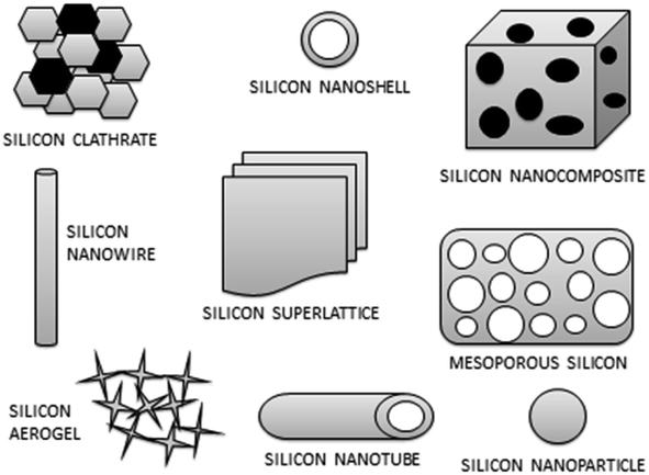 | ||
| Fig. 6 Example classes of silicon nanostructures. | ||
A variety of different terms for luminescent silicon nanostructures are used in the literature, so we will start by mentioning them here. The terms silicon “quantum” wells, wires, and dots are the smallest 1D, 2D and 3D confined crystalline silicon structures, respectively, with diameters below that of the Bohr exciton radius (∼4 nm) in bulk silicon (see Section 1.3). Such structures are expected to have bandstructures that are size-dependent due to quantum confinement effects as discussed in Section 1.6. Silicon “nanoparticles”, nanowires, nanopillars or nanorods can often, but not always, have larger diameters in the range 5–100 nm. These can exhibit carrier confinement effects on PL but their bandstructure is similar to that of bulk Si. In the literature both terms are used interchangeably. “Nanoclusters”, for example, often denote the tiniest structures consisting of under 50 atoms. Likewise, “nanosheets” usually refer to free-standing layers of, at most, a few atoms thickness.
The experimental literature is currently dominated by luminescent silicon nanocrystals, porous silicon, silicon nanowires and silicon superlattices, in that order. The theoretical literature is dominated by calculations of silicon quantum wires and silicon quantum dots. Other silicon nanostructures have received some, but not substantial development. Examples of silicon nanostructures where efficient visible luminescence at 300 K is either not reported or not quantified to date include silicon nanoribbons,49 nanoshells and nanotubes,50 nanosheets,51–54 molecular clusters,55 allotropes56 and metastable polymorphs.57
1.6. Theory of quantum confinement effects in Si nanostructures
Theoretical studies of how the silicon bandstructure evolves with size and shape in the critical 1–10 nm size range began in the early 1990s and there is now a substantial body of work. I am not aware of a prior review that tries to comprehensively analyze the considerable theoretical literature on silicon nanostructures and will not attempt to here. Numerous publications are provided here and a few concepts and trends are selected where there is a consensus with respect to issues that affect PLQY, PLWT and PLDT of silicon nanostructures.Starting with the earliest calculations in 1992–1993 (ref. 58–60) and many others, theoretical work has continuously grown over the last 30 years, due to a myriad of potential applications for nano-Si, many of which do not utilize photoluminescence. Studies are grouped in Table 2, not by calculation technique, but by nanostructure morphology and surface/interface chemistry. The aim is to help readers access the available theory most relevant to their specific luminescent nanostructures. A large number of theoretical studies have focused on silicon quantum wires, but the literature on quantum dots is growing. Luminescent porous silicon has been modelled as idealized quantum wires and quantum dots or by introducing an artificial periodicity of holes via supercell techniques.109 In reality, morphology is variable but often of mixed 2–3D confinement due to undulating wire thickness (see Section 2.1) combined with other geometrical shape variations.110
| Model nanostructure morphology | Surface chemistry | Size range studied | References |
|---|---|---|---|
| Quantum slabs (free-standing) | Si–Hx | 0.3–6.0 nm | 61–64 |
| Quantum wells (embedded) | Si–SiOx, Si–CaF2 | 0.3–6.0 nm | 65–69 |
| Quantum wires (free-standing) | Si–Hx | 0.8–3.0 nm | 70–85 |
| Quantum wires (core–shell) | Si–SiOx | 1.0–3.0 nm core | 86–88 |
| Quantum wires | Si–CH3 | 1.0–3.0 nm | 89 |
| Quantum dots | Si–Hx | 1.0–5.0 nm | 74 and 90–94 |
| Quantum dots | Si–SiOx | 1.0–5.0 nm | 95–99 |
| Quantum dots | Si–organic ligands | 1.0–5.0 nm | 100–106 |
| Ultrasmall Si clusters | Si–Hx | 1–50 atoms | 107 and 108 |
Surveying the theoretical data of Table 2 there would appear to be a consensus that:
• The silicon bandgap starts to widen significantly for quantum wells (slabs/nanosheets) with widths under 2 nm, quantum wires with diameters under 3 nm and quantum dots with diameters under 5 nm.
• In principle the entire visible range is accessible for quantum dots and wires, with bandgap tunability extending from 1 eV to 3 eV.
• Exciton binding energy is significantly enhanced due to quantum confinement reaching values as high as a few hundred meV for 1.5–3 nm diameter quantum dots or 1–2 nm diameter quantum wires.
• Surface chemistry significantly affects the bandstructure of smaller nanostructures, e.g. oxidation narrows the bandgap of hydride passivated nanostructures.
Table 3 provides some theoretical data for hydride passivated silicon quantum dots, quantifying how the bandgap and strength of exciton binding increase dramatically with decreasing size for 1–5 nm nanocrystals. Note how the predicted radiative recombination rates however, only become comparable with those of direct bandgap semiconductors for the smallest silicon nanocrystals around 1 nm diameter.
| Size | 1 nm | 1.5 nm | 2.0 nm | 2.5 nm | 3.0 nm | 3.5 nm | 4.0 nm | 5.0 nm | References |
|---|---|---|---|---|---|---|---|---|---|
| Number of silicon atoms | 29 | 87 | 191 | 389 | 705 | 1087 | >1500 | >3000 | 111 |
| Number of hydrogen surface atoms | 36 | 76 | 148 | 254 | 300 | 436 | >500 | >750 | 112 |
| Excitonic bandgap (eV) (nm) associated spectral range | >3.5, <354, UV | >2.5, <496, blue | 2.2, 563, green | 1.9, 653, red | 1.7, 729, red | 1.6, 775, near IR | 1.5, 827, near IR | 1.35, 918, near IR | 112 |
| Exciton binding energy (meV) | ∼400 | ∼300 | 200 | 160 | 125 | 95 | 113 and 114 | ||
| Radiative recombination rate (s−1) | >107 | ∼106 | ∼105 | ∼104 | <104 | 115 |
Aside from size, shape and surface chemistry, there are other factors that affect bandstructure and therefore PL. There have, for example, been a series of theoretical effects investigating the roles of strain.116–119 For quantum wires, crystallographic orientation also has a significant effect on bandstructure.75,77,83,120
1.7. PL quantum yield (PLQY)
For any photoluminescent material or molecular species the efficiency of its radiative processes or “photoluminescence quantum yield” (PLQY) of its luminescence is an important quantitative property that will impact on its likely use. The PLQY depends on direct competition between the specific radiative process and all non-radiative processes:| PLQY (%) = photons emitted/photons absorbed = kr/(kr + Σknr) | (2) |
Measurement of both PLQY η and luminescence decay time τPL enables one to separate the radiative and non-radiative lifetimes of excited states using the simple relation
| PLQY = η = τPL/τr = 1/τr/(1/τr + 1/τnr) | (3) |
The intrinsic radiative recombination coefficient kr of bulk c-Si has been estimated to be 2 × 10⁻¹⁵ cm3 s−1 which is about 100000 times lower than direct bandgap semiconductors like GaAs. Absolute quantum efficiency estimates of interband recombination (see Fig. 2) in standard silicon crystals (wafers) with native oxide surfaces (see Table 1) typically range from 10−6 to 10−4. However, eqn (3) emphasizes that if all non-radiative processes can be virtually removed, then PLQY can be quite high. This has been elegantly demonstrated by solar cell specialists (Green and co-workers). In 2003 they showed that in the highest purity float zone silicon with optimized surface passivation, PLQY of near infrared emission could be as high as 6.1 ± 0.9% at 300 K.121
Accurate measurement of PLQY is not as straightforward as measuring PL decay times and a number of different protocols exist, but they can be divided into comparative ones that utilize photoluminescence standards of known PLQY and absolute ones that directly measure the fraction of absorbed photons that are emitted as photoluminescence or the fraction of photons lost by non-radiative recombination. The latter use integrating spheres to collect all emitted light, or use photoacoustic/calorimetric methods to quantify heat production. Methodology can depend on the physical form of the photoluminescent material (e.g., film versus dry powder versus colloidal solution) and the spectral positions of both excitation and emission. A number of important reviews are available that detail the theory, methodologies, standards, and sources of error involved.122–127 Of particular relevance here is the review by Valenta on PLQY measurements of nanomaterials.127
For comparative methods, the most established standards are quinine sulphate in 0.5 M sulphuric acid, fluorescein in 0.1 M NaOH and rhodamine 6G in ethanol with peak emissions at 451, 515 and 552 nm, respectively. Their PLQY accuracy is better than 4% under well-defined conditions.124 These standards are well suited to the spectral positions of the F-band (see Section 3).
The physical form of silicon nanostructures can have a pronounced effect on PLQY. For example, for thin solid films light entrapment effects due to total internal reflections and Fresnel transmission at the film–air interface can dramatically lower PLQY, even if the internal quantum efficiency (IQE) is very high. A light extraction efficiency ExPL for a thin film on an absorbing substrate has been estimated.128 The escape probability of emitted light is strongly dependent on refractive index:
| ExPL = 1/[nc(nc + 1)2] | (4) |
So, for example, with a solid silicon film of refractive index 3.5 only 1.4% of light escapes directly from the top surface. For silicon nanocrystals embedded in silica films with a refractive index of 1.64, only 8.7% escapes internal reflections. For porous silicon nanostructures, PLQY and IQE values start to get closer as refractive index is lowered. High PLQY pSi structures have porosities in the range 70–90% with refractive indices as low as 1.1. Now more than 20% of light emitted internally can directly escape, lowering its self-absorption. Forming luminescent nanocomposites will often normally lower the perceived brightness due to refractive indices then being higher again.
Table 4 collates the highest PLQY values reported to date for all types of silicon nanostructure. It is clear that the highest PLQY values have been obtained in colloidal quantum dots, quantum dot-based superlattices and porous silicon and so these materials are given more consideration in this review. Amorphous nanoparticles have much lower PLQY than crystalline ones and are therefore not discussed. Molecular size clusters and size-dependent PL from ultrathin quantum wells have not had PLQY quantified to date. Nanotube studies have not reported visible PL.
| Class of nanostructure | Structure details | PL peak position | PL efficiency (PLQY at 300 K) and PL band (F or S) | References |
|---|---|---|---|---|
| Si QDs (?) | 4 nm NPs and fluorescein ligands in colloidal solution | 522 nm, 2.38 eV | 90% (F) | (Zhong 2019)129 |
| Si QDs (?) | 5 nm NPs and arylamine ligands in colloidal solution | 555 nm, 2.23 eV | 90% (F) | (Li 2016)130 |
| Porous silicon nanoparticles | 3 nm alkyl-Si NCs in colloidal solution | 740 nm, 1.87 eV | 68 ± 5% (S) | (Yuan 2017)131 |
| Si QDs | 3 nm alkyl–Si NCs in colloidal solution | 638 nm, 1.94 eV | 66 ± 8% (S) | (Yang 2015)132 |
| Si QD-based nanocomposites | 4.5 nm alkyl–Si NC in polymer matrix | 775 nm, 1.6 eV | 65 ± 5% (S) | (Marinins 2017)133 |
| Si QDs | 5 nm methyl–Si NC colloidal solution | 775 nm, 1.6 eV | 65 ± 6% (S) | (Sangghaleh 2015)134 |
| Si QDs | 4 nm octadecyne–Si NC colloidal solution | 789 nm, 1.57 eV | 62 ± 11% (S) | (Jurbergs 2006)135 |
| Si-QD based superlattices | Embedded 4.5 nm NC with 3 nm silica barriers | 992 nm, 1.25 eV | 50% (S) | (Valenta 2019)136 |
| Porous Si microparticles | SCD pSi with <3 nm interlinked NCs and 1150 m2 g−1 | 685 nm, 1.81 eV | 32% (S) | (Joo 2016)137 |
| Si nanorods (?) | ∼20 nm wide NWs | 500 nm, 2.48 eV | 15% (F) | (Song 2016)138 |
| Si nanosheets (?) | Buckled silicon monolayers | 500 nm, 2.48 eV | 9% (F) | (Ryan 2019)139 |
| Porous Si nanowires | 20–200 nm wide NWs with interlinked 3 nm NCs | 740 nm, 1.68 eV | 5% (S) | (Gonchar 2012)140 |
| Solid Si quantum wires | 3–4 nm wide NWs | 730 nm, 1.70 eV | 4.3% (S) | (Lu 2013)141 |
| a-Si:Ox QDs | Embedded 2 nm NPs in oxide | 600 nm, 2.07 eV | 1–4% (S) | (Goni 2014)142 |
| a-Si:H QDs | Embedded 3–5 nm NPs | 850 nm, 1.46 eV | <2% (S) | (Anthony 2009)143 |
| Solid Si quantum wires | 5 nm Si NWs | 750 nm, 1.65 eV | 0.5% (S) | (Irrera 2012)144 |
| Si quantum wells | 1.1–2.7 nm layers with silica barriers | 700 nm, 1.77 eV, 912 nm, 1.36 eV | — | (Cho 2007)145 |
| Si molecular clusters | Octasilacubane (Si8)–butyldimethylsilyl crystal | 751 nm, 1.65 eV | — | (Kanemitsu 1995)55 |
| Si nanosheet nanocomposite | Si6 H6 sheets in polystyrene | 510 nm, 2.43 eV | — | (Helbich 2016)146 |
| Solid Si nanotubes | 3–7 nm c-Si tubular walls | — | — | (Tang 2005)50 |
2. S-Band photoluminescence
2.1. Porous Si (2D to 3D confinement)
Historically, relatively efficient (∼3%) S-band emission at room temperature was first observed in high porosity silicon47 which is why we first consider this nanostructure, despite its complex range of morphologies which make theoretical modelling a challenge. Freshly etched red-emitting high porosity silicon was found to contain “undulating” quantum wires147 of below 3 nm average width (Fig. 7b). | ||
| Fig. 7 (a) S-band PL tuning via porosity of hydride passivated porous silicon.148 Reprinted and adapted with permission from M. V. Wolkin, J. Jorne, P. M. Fauchet, G. Allan and C. Delerue, Phys. Rev. Lett., 82(1), 197–200, 1999. Copyright 1999, the American Physical Society. (b) Complex morphology of photoluminescent porous silicon of 78% porosity.147 Adapted with permission from A. G. Cullis and L. T. Canham, Nature, 353, 335–337, 1991. Copyright 1991, Nature Publishing Group | ||
Efficient S-band emissions are also evident in material where hydride passivation is replaced by native oxides,137,149 anodic oxides,150 high temperature oxides30 and organic monolayers.151 All these surface chemistries, with the notable exception of native oxides in some cases (see Table 1) produce low levels of non-radiative surface recombination in bulk Si. In oxide-free material tuning from the near infrared to the blue spectral region (1300 to 400 nm) has been achieved, as shown in Fig. 7a.148,152 In oxidized material, from the near infrared to the yellow (1300 to 590 nm).148 Typical PL lifetimes (see Table 5) are in the microsecond range but depend on wavelength and surface passivation quality (SRV) (see eqn (3)).
| Wavelength (nm) | Energy (eV) | Decay time (μs) | Decay time (μs) | Decay time (μs) | Decay time (μs) | Decay time (μs) | Decay time (μs) |
|---|---|---|---|---|---|---|---|
| Surface passivation | Native oxide | Native oxide | Hydride | Native oxide | SCD native oxide | HP wet oxide | |
| References | 153 | 154 | 152 | 155 | 137 | 156 | |
| 800 | 1.55 | 10 | 20 | 50 | 65 | 100 | |
| 700 | 1.77 | 9 | 10 | 12 | 30 | 42 | 50 |
| 600 | 2.07 | 2.5 | 5 | 9 | 12 | 20 | 20 |
| 550 | 2.25 | 1.5 | 1 | 3 | 10 | ||
| 500 | 2.48 | 0.7 | 2.5 | ||||
| 450 | 2.76 | 0.1 | 0.2 | ||||
| 400 | 3.10 | 0.02 |
The data in Table 5 shows variability in PLDT at given wavelengths, due to differing silicon skeleton morphology and interconnectivity, levels of polycrystallinity and surface passivation. Nonetheless, the longest PLDT values of Gelloz 2005 probably reflect primarily the lowest SRV values obtained to date by their wet oxide passivation technique.
2.2. Single quantum wells and nanosheets (1D confinement)
Takahashi et al.157 and Saeta et al.158 were the first to report visible emission from single 2D crystalline silicon structures. Both groups used SIMOX wafers, thinning the silicon layer with high precision via thermal oxidation. A red and near infrared emission band (1.65 eV) was observed with an intensity dependent on the well thickness but spectral position varying little. No luminescence was observed unless the quantum well thickness was less than 5–8 nm. PLQY peaked at ∼2 nm thickness but was very low at 10−4.158,159 Okamoto et al.160 reported 2 K PL from SIMOX-derived quantum wells of only 0.6 and 1.6 nm. Emission was again at 1.66 eV. Pauc et al.161 studied PL at 6 K from SIMOX derived wells of 3.9 down to 0.6 nm. A 1.6 eV band appeared for the narrowest wells with an estimated PLQY of only 0.1% at 6 K.The first really size-tunable emission was achieved by Green and co-workers.162 They used ELTRAN structures with superior defect densities (<50 cm−2), atomically flat interfaces and lower SRVs. Fig. 8 shows TEM data and the 650–950 nm PL spectra as a function of well thickness over the range 1.1–2.7 nm. Their data on processed SIMOX wafers also reported an emission whose peak wavelength was insensitive to QW thickness but correlated instead with oxide thickness. Zhu et al.163 studied (110) SIMOX wafers with ∼1–4.4 nm thick wells. Both QC and interface effects were discussed in relation to their 750–800 nm emission. Wagner et al.68 also achieved size dependent 75 K emissions over 1.6 to 1.2 eV for 1–4 nm well widths.
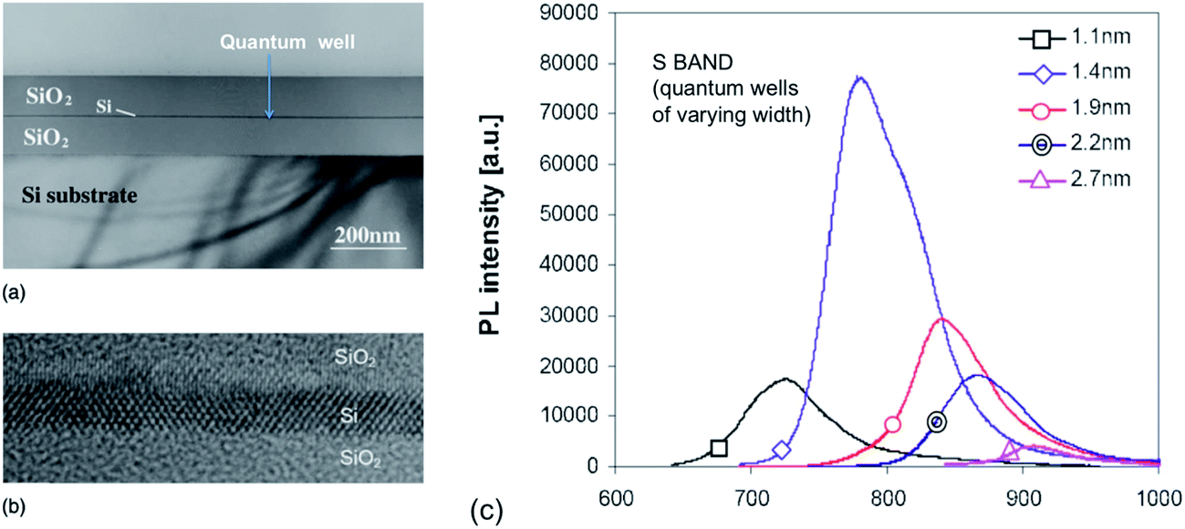 | ||
| Fig. 8 Single silicon quantum well and associated S-band PL for varying well thickness.162 Reprinted and adapted with permission from E. C. Cho, M. A. Green, J. Xia, R. Corkish, P. Reece, M. Gal and S. H. Lee. J. Appl. Phys., 2007, 101, 024321. Copyright AIP Publishing. | ||
2.3. Superlattices and multilayers (1D to 3D confinement)
Multilayer and superlattice structures have primarily been based on silica passivation,164–171 but photoluminescent lattice matched Si/CaF2 superlattices172–174 have also been achieved. Lockwood and co-workers164,165 first reported a photoluminescent MBE grown Si/SiO2 superlattice. The 6 period structure had 1.0–5.4 nm thick Si quantum wells with 1 nm thick oxide barriers. Visible emission was only observed for wells below 3 nm. PL peak energies were tunable over the 1.7–2.3 eV range but PLQY values were not given. A major advance was made by the Zacharias group in a series of papers171,175,176 using superlattices to exploit 3D rather than 1D confinement. They also dramatically raised PLQY via improved interface passivation, size control and nanocrystal density. Fig. 9 shows a typical structure and the tunability of the PL.171 Valenta et al.176 provided detailed information on PLQY values, lying in the range 10–20% and doubling when the silica barrier layer thickness was increased from 1 to 3 nm. PLQY variation with temperature was also studied, peaking at 30% at 100 K. Very recently,136 PLQY values reported for near infrared emission (1.35 eV/0.97 micron) corresponding to 4.5 nm nanocrystals were as high as 50%.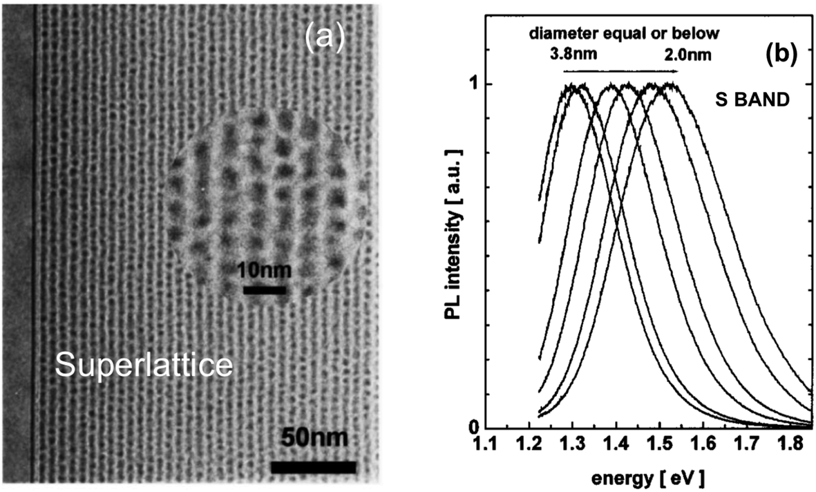 | ||
| Fig. 9 Superlattice-based nanocrystals and their S-band photoluminescence.171 Reprinted and adapted with permission from M. Zacharias, J. Heitmann, R. Scholz, U. Kahler, M. Schmidt and J. Blasing, Appl. Phys. Lett., 2002, 80(4), 661–663. Copyright AIP Publishing. | ||
2.4. Nanowires and quantum wires (2D confinement)
The first free-standing isolated NWs of widths under 10 nm realized by lithographic etching techniques showed very weak photoluminescence177–179 or no visible luminescence at all, ascribed to insufficient surface passivation.180 Using laser ablation to create 13 nm wide ultralong nanowires, and then oxidation to thin the silicon core to 3.5 nm, Feng and co-workers reported red emission of unknown PLQY.181 Complete oxidation of the wires removed the red emission but a distinct green emission band persisted (see Section 3.2). Brongersma and co-workers used catalysed CVD growth to create 20 nm wide nanowires and then oxidation to decrease core widths to below 5 nm. Tunable 800 to 720 nm emission with microsecond decay times was achieved.182Examination of Table 4 reveals that nanowire fabrication, excluding porous silicon, has been less successful to date with regards to achieving the highest PLQY values for S-band emission. Korgel’s group reported a PLQY of 4.3% for 3–4 nm wide solid quantum wires.141 For nanowires we need to distinguish those that are solid silicon from those that have larger diameters but are themselves porous. The latter “porous silicon nanowire arrays” will behave in a similar manner to porous silicon films but with lowered nanocrystal densities and, to date, lower PLQY (see Table 4). Some much larger solid nanowires also have oxidized rough sidewalls containing nanocrystals that generate the visible photoluminescence.183
Fig. 10 shows an energy filtered TEM image of ultrathin luminescent solid quantum wires reported recently.184 These were extracted by-products of a plasma torch spherodization of micro-particulate powder. Once extracted via centrifugation, the various fractions showed PL that shifted from 950 to 680 nm as the average Si core diameter evolved from ∼5 to ∼3 nm.
 | ||
| Fig. 10 Luminescent ultrathin silicon nanowires from plasma synthesis and their S-band 300 K PL at varying levels of surface passivation.184 Adapted with permission from V. Le Borgne, M. Agati, S. Boninelli, P. Castrucci, M. de Crescenzi, R. Dolbec and M. A. E. Khakani, Nanotechnology, 2017, 28, 285702. Copyright IOP Publishing. All rights reserved. | ||
2.5. Nanoparticles and quantum dots (3D confinement)
S-band PL from visibly luminescent silicon nanocrystals (nanoparticles) synthesized by a broad range of techniques have now received a vast amount of study. Fabrication techniques include plasma-assisted decomposition of silane or silicon tetrachloride; laser pyrolysis of silane; liquid phase synthesis; laser ablation; high energy milling and microemulsion growth. The reviews of Mangolini,185 Huan et al.186 and Cheng et al.187 provide details on the majority of these synthesis techniques. Highlighted here is the recent study of the Ceroni and Korgel Groups using dodecene passivated nanocrystals in colloidal suspension.188Fig. 11 illustrates the excellent control over size. Fig. 12 shows how spectral position smoothly “blueshifts” with decreasing nanocrystal size right from the 1.1 eV bandgap of bulk silicon (for 9.1 nm average size) to 2.1 eV (1.8 nm average size).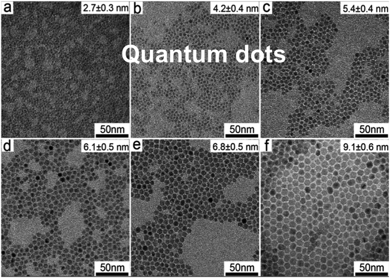 | ||
| Fig. 11 S-band photoluminescent silicon nanocrystals of controllable size.188 Adapted with permission from Y. Yu, G. Fan, A. Fermi, R. Mazzaro, V. Morandi, P. Ceroni, D. M. Smilgies and B. A. Korgel, J. Phys. Chem. C, 2017, 121, 23240–23248. Copyright 2007 American Chemical Society. | ||
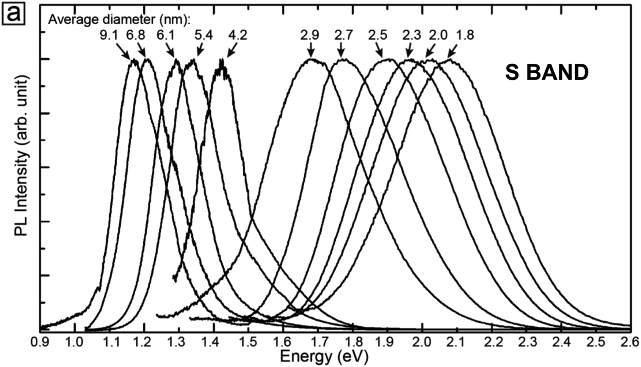 | ||
| Fig. 12 S-band 300 K PL from the various-sized nanocrystals of Fig. 11.188 Adapted with permission from Y. Yu, G. Fan, A. Fermi, R. Mazzaro, V. Morandi, P. Ceroni, D. M. Smilgies and B. A. Korgel, J. Phys. Chem. C, 2017, 121, 23240–23248. Copyright 2007 American Chemical Society. | ||
Table 6 shows the decay times from a number of nanocrystal studies and it is informative to compare values therein with Table 5 (data from porous silicon). For example, at 800 nm, pSi decay times (Table 5) lie in the range 10–100 microseconds; isolated nanocrystals emitting at 800 nm (Table 6) have much longer decay times in the range 80–247 microseconds. It is likely that the internal surfaces of porous silicon nanostructures are more challenging to passivate than isolated or embedded nanocrystals.
2.6. PLQY of S-band
Table 7 summarizes the remarkable improvements made in raising the PLQY of S-band luminescence alone since 1990. Early values in the range 3–5% probably reflected the lower levels of size control, combined with higher SRV levels. The highly interconnected silicon skeleton of porous silicon facilitates rapid exciton migration to lower bandgap parts of the network that have slower radiative rates.137,193 Size control is thus key. This, in combination with differing light extraction efficiencies, explains why colloidal pSi nanoparticles typically have higher PLQY than microparticles and films (see Table 7).| Maximum PLQY (%) | Nanostructure | Peak PL wavelength (nm) | Mean size/size range (nm) | Surface chemistry | Fabrication technique | References |
|---|---|---|---|---|---|---|
| 68 | pSi NPs | 740 | 3 | Dodecyl | pSi ablation | (Yuan 2017)131 |
| 66 | NP | 700 | 3 | Dodecyl | HSQ decomposition | (Yang 2015)132 |
| 65 | NP | 690 | 4 | Native oxide | Silane pyrolysis | (Potrick 2011)194 |
| 62 | NP | 789 | 4 | Octadecene | Plasma synthesis | (Jurbergs 2006)135 |
| 62 | NP | 825 | 4 | High pressure wet oxide | Plasma synthesis | (Gelloz 2019)192 |
| 50 | SL | 954 | 4.5 | Thermal oxide | PECVD | (Valenta 2019)136 |
| 60 | NP | 775 | 3 | Dodecyl | HSQ decomposition | (Sanggahelah 2015)134 |
| 59 | NP | 750 | 2 to 3 | Thermal oxide | Ion implantation and anneal | (Walters 2006)195 |
| 45 | NP | 827 | 3.5 | Dodecene | HSQ decomposition | (Yu 2017)188 |
| 43 | NP | 760 | 1.9 to 2.5 | Allylbenzene | HSQ decomposition | (Mastronardi 2011)196 |
| 32 | pSi particles | 685 | <2.5 | Native oxide | Anodisation and supercritical drying | (Joo 2016)137 |
| 31 | pSi films | 735 | <2.7 | High pressure wet oxide | Anodisation | (Gelloz 2019)192 |
| 30 | NP | 600–850 | 2 to 7 | Native oxide | Laser pyrolysis | (Ledoux 2002)200 |
| 25 | NP | 650 | 1.6 | Allylbenzene | HSQ decomposition | (Mastronardi 2011)196 |
| 19 | SL | 950 | 4.5 | Thermal oxide | PECVD | (Valenta 2014)176 |
| 0.3 | SL | 1170 | 12 | Thermal oxide | Sputtering | (Zacharias 1998)197 |
| 5 | NP | 600–800 | 1 to 2 | Thermal oxide | Disilane pyrolysis | (Brus 1995)198 |
| 3 | pSi films | 700–850 | 2 to 10 | Anodic oxide | Electrochemical etch and oxidation | (Vial 1992)150 |
| 3 | pSi films | 750–850 | 2 to 10 | Hydride | Electrochemical etching | (Canham 1990–1991)47 |
2.7. Wavelength tuning of S-band via nanostructure size and shape
A wealth of data now exists confirming that S-band spectral position depends on size distribution for a variety of nanostructures: 1.1–2.7 nm quantum wells within oxide;162 3–5 nm quantum wires from plasma synthesis;184 3–8 nm nanocrystals from disilane pyrolysis;199 3.4–4.8 nm nanocrystals from silane pyrolysis;200 3–8 nm and 4–9 nm nanocrystals embedded in silica via sputtering;200–202 2–5 nm nanocrystals embedded in silica via ion implantation;203 1.5–4 nm nanocrystals embedded in silica via PECVD;204 and hydride passivated porous silicon of varying porosity.47,148,152,205–207Fig. 13 presents a published and very useful compilation of PL data from 17 studies on nanocrystals made by a variety of techniques208 and effective mass approximation (EMA) fitting of nanocrystal bandgap versus size. There is clearly considerable scatter of quantitative data, partly because both S-band (this section) and F-band (see Section 3) data were used. For the S-band data, another complicating factor are the size-dependent optical absorption coefficients: smaller silicon nanocrystals have lower optical absorption which biases the PL spectra towards larger nanocrystals.188Fig. 14 illustrates how one parameter (nanocrystal size dispersion) can therefore strongly influence the theoretical EMA modelling of PL tunability versus average size. Good agreement between such theory and experimental data is achieved once this is taken into account.
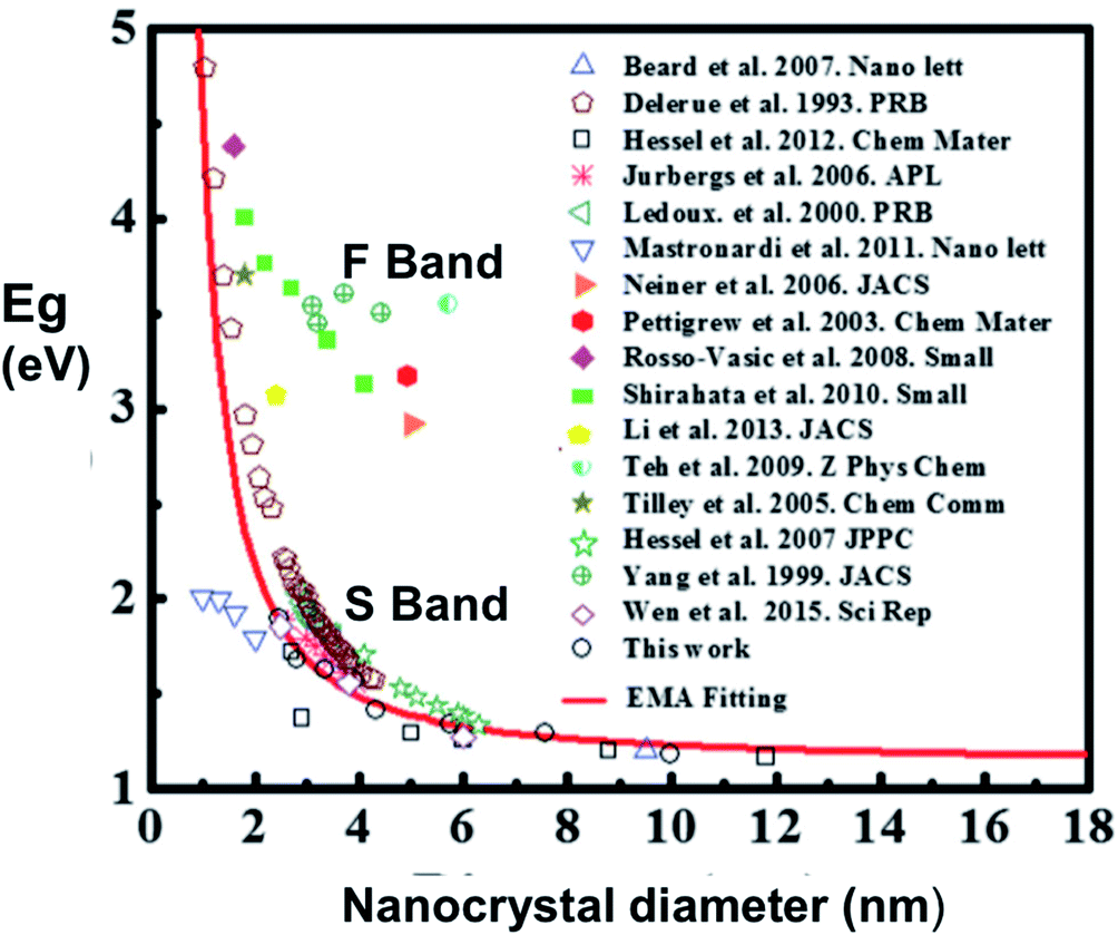 | ||
| Fig. 13 Size dependence of photoluminescence for silicon quantum dots.208 Reprinted with permission from X. Liu, Y. Zhang, T. Yu, X. Qiao, R. Gresback, X. Pi and D. Yang. Part. Part. Syst. Charact., 33(1), 44–52, 2016. Copyright 2015, WILEY-VCH Verlag GmbH & Co. KGaA, Weinheim. Some of the featured studies reported F-band data rather than S-band data, as highlighted here. | ||
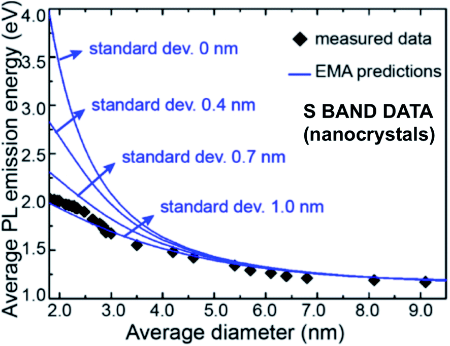 | ||
| Fig. 14 Effective mass approximation (EMA) modeling of S-band spectral position versus nanocrystal size for various levels of size polydispersity (standard deviations).188 Adapted with permission from Y. Yu, G. Fan, A. Fermi, R. Mazzaro, V. Morandi, P. Ceroni, D. M. Smilgies and B. A. Korgel, J. Phys. Chem. C, 2017, 121, 23240–23248. Copyright 2007, American Chemical Society. | ||
2.8. Wavelength tuning of S-band via surface chemistry
The ability to tune PL emissions by surface chemistry passivation, as well as by nanostructure size, would be desirable, particularly for fabrication techniques which offered high volume throughput, but lacked fine tunability of size. Theoretical calculations have shown that the bandstructure of ultrasmall nanostructures such as 1–1.5 nm diameter quantum dots and quantum wires are strongly affected by surface chemistry.86,95,96 Spectral position of the S-band might then also be tunable by surface chemistry. However direct experimental evidence for extensive S-band tuning is sparse. One study reported that for larger nanocrystals (1.64 eV PL corresponding to ∼3.5 nm nanocrystals) changing from hydride to alkyl (dodecene) passivation had little effect on spectral position.209 Not surprisingly however, PLQY and PLDT were affected, as the SRV will differ. In contrast, a study of amide and alkoxy functionalization relative to alkyl did find a small but measurable effect on spectral position for 3.5–6.4 nm nanocrystals.210 In addition, another study using alkynyl(aryl) groups also observed PL shifts (in the range 685–800 nm). They attributed the effect to “surface-state induced bandgap changes”.211 In instances where chemical tuning “right across the visible range” is claimed for silicon nanocrystals,212,213 it would be important to investigate whether the blue emission is in fact F-band emission by measuring PLDT as a function of tuning (see Section 3) and therefore of quite different origin to the yellow or red S-band emission. The extent to which the S-band can be tuned over a broad wavelength range via surface chemistry alone needs further investigation.2.9. Selective photoexcitation of S-band emission
As we saw with many radiative transitions in bulk silicon (Section 1.3), sharp features in PL spectra can allow the determination of precise energies of electronic states, the symmetry of luminescent defects and the phonon energies involved. The large linewidth of the S-band PL obscures the spectroscopic information it contains. Photoexcitation at resonant wavelengths via tunable lasers can selectively excite subsets of the nanocrystal ensemble and lower the effects of inhomogeneous broadening, thereby revealing otherwise hidden spectral features. Starting with the studies of Calcott, Nash and co-workers it has now been investigated extensively with luminescent porous silicon198,214–222 but also with silicon superlattice nanocrystals,223,224 large silicon nanowires,225 quantum wells226 and nanocrystals made by various other techniques.198,227–230 Initial concerns raised about its applicability to high PLQY porous silicon emission at room temperature and the precise number of phonon features were resolved by 1997.30 Highlighted here in Fig. 15 are S-band resonant photoexcitation data from a range of different silicon nanostructures. All show the TO and TA phonon-related features so characteristic of exciton recombination in crystalline silicon. For the S-band PL from a given nanostructure, at increasing levels of confinement (shorter wavelength emission), the exciton binding energy increases (Table 3) and the no-phonon (NP) to phonon (TO, TA) intensity ratio increases, just as for localized bound excitons in bulk silicon (Fig. 3 and 4).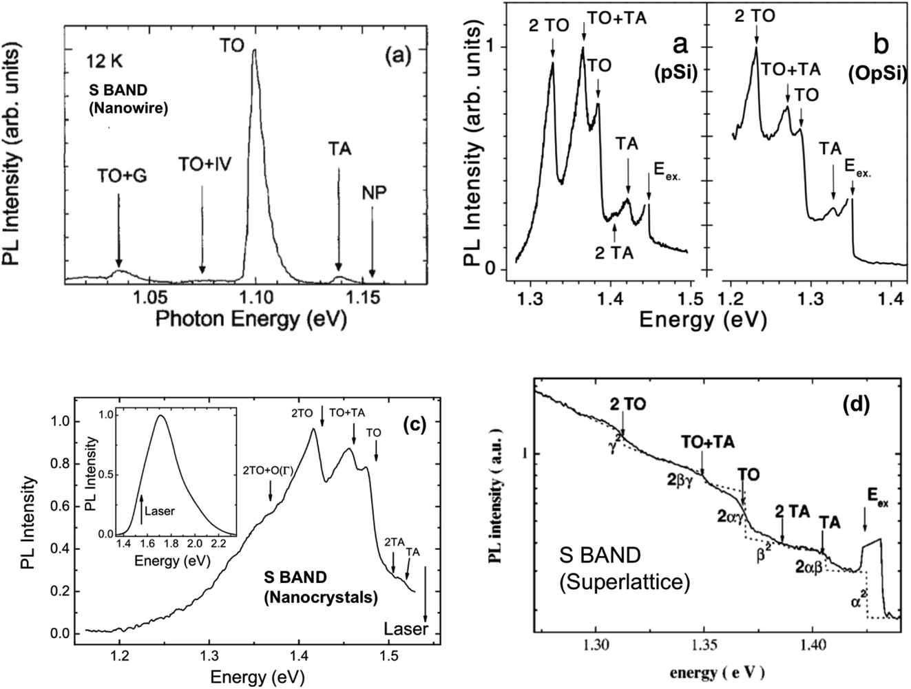 | ||
| Fig. 15 Resonant photoexcitation of silicon nanostructures. (a) Large silicon nanowires,225 (b) freshly etched porous silicon (pSi) and oxidized porous silicon (OpSi),228 (c) free standing silicon nanocrystals,230 (d) silicon nanocrystals embedded in oxide-based superlattice.224 Adapted with permission from Y. Kanemitsu, H. Sato, S. Nihonyanagi and Y. Hirai, Phys. Stat. Solidi, 190, 755–758, 2002; D. Kovalev, H. Heckler, M. Ben-Chorin, G. Polisski, M. Schwartzkopf and F. Koch, Phys. Rev. Lett., 1998, 81(13), 2803–2806; B. Goller, S. Polisski, H. Wiggers and D. Kovalev, Appl. Phys. Lett., 2010, 97, 041110 and J. Heitman, F. Muller, L. Yi, M. Zacharias, D. Kovalev and F. Eichhorn, Phys. Rev. B, 2004, 69, 195309, respectively. | ||
Even more revealing than resonant photoexcitation can be the photoexcitation of isolated individual nanostructures. Single nanostructure spectroscopy can reveal homogeneous linewidths and most previously hidden spectral features, but is experimentally challenging. The first such spectroscopy studies were performed on porous silicon particles in 1998 by Buratto and co-workers.231 Progress has been recently thoroughly reviewed by the Linnros group232 so only a few comments will be made here that relate to PLQY of nanostructure ensembles and the origin of S-band PL:
• Individual nanocrystals “blink” (periods of no emission under constant photoexcitation) and some are completely “dark”; others are “bright” with near unity IQE. The ensemble PLQY can thus be raised significantly by lowering the density of dark silicon nanocrystals that have a very efficient non-radiative channel(s), by decreasing blinking rates, or by both routes.
• PL linewidths for single nanocrystals are substantially narrower than for the ensemble (typically 100–160 meV at 300 K but values as low as 17 meV are now being reported233). Both temperature and the medium surrounding the core have a strong influence.
• Substantial TO phonon involvement was again invoked to explain the emission spectral data.
2.10. Origin of S-band PL
The wavelength tuning via size (Section 2.7), right from the bulk silicon bandgap201,205 to at least the yellow spectral region, convinced many that quantum confinement was indeed responsible for S-band emission. Resonant photoexcitation experiments (Fig. 15), providing a spectroscopic signature of established silicon phonon-assisted transitions (Section 1.3), convinced many more. Single nanocrystal spectroscopy (Section 2.9) holds the most potential for unravelling the complexity of ensemble nanosystems where size and shape control is still improving, but not yet sufficient to avoid significant inhomogeneous broadening and rapid carrier migration effects.234 Nonetheless, after many hundreds of studies, there is now substantial evidence, both experimental and theoretical, supporting a quantum confinement model for S-band emission, at least for near infrared to green emission. Agreement between theory and experiment exists for PL position (excitonic bandgap) versus size and shape (Fig. 14), together with strongly wavelength-dependent measured decay times (Tables 5 and 6) and extracted radiative decay times. The reasons for rapid decline in PLQY for yellow to blue S-band emission; the ultimate PL linewidths achievable; the avoidance of “blinking”; improvements in SRV for smaller nanostructures – these are all topics requiring further study.3. F-band photoluminescence
3.1. Porous Si
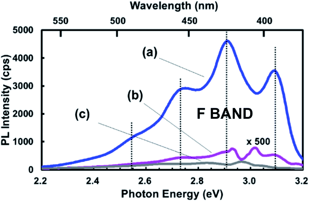
Reports of blue–green emission (“fast”-nanosecond decay time and hence “F-band emission”) from porous silicon started to appear235,236 in 1992. Kovalev and co-workers237 showed that its intensity could be significantly raised by rapid thermal oxidation and since then it has received a series of studies. It is noteworthy that even moderate PLQY requires oxidation238 and/or heat treatment of the porous silicon. Freshly oxidized porous silicon often does not display F-band emission and it only emerges after storage in ambient air.2393.2. Nanowires
Growth of nanowires via catalyzed laser ablation VLS growth or thermal evaporation often results in short wavelength emission alone.240–244 A silicon oxide phase is invariably present and often silicon core width greatly exceeds that required for silicon bandgap enlargement (<3 nm). Sometimes there is no silicon phase at all.240 PLQY values have not generally been provided.3.3. Nanoparticles and quantum dots
For silicon quantum dots prepared by high temperature synthesis, such as silane decomposition, F-band emission also appears after air storage (see Fig. 1).A very large number of reports of F-band emission of high PLQY (only some are in Table 8) have appeared since the 2013 report of “one-pot aqueous synthesis”245 by He and co-workers. Here, efficient blue–green emission is achieved immediately after reduction synthesis using inexpensive precursors, low temperatures (e.g. <200 °C) and short reaction times. Highlighted here though instead, is the recent reappraisal study of Oliinyk and co-workers.246 They cast doubt on the likelihood of such conditions generating crystalline silicon nanostructures. Importantly, they also report that repeating the synthesis with a control (reducing agent and a silicon-free organic amine) produced remarkably similar photoluminescence. The de Cola group have also repeated such a synthesis under both short (15 minute) microwave irradiation and lengthy (300 minute) hydrothermal conditions.247 After thorough characterization of repeat and control formulations (lacking reducing agent or silicon source) they attribute the blue-emitting product to the formation of silica and carbon dots rather than silicon nanocrystals.
| Maximum PLQY (%) | Peak PL wavelength (nm) | Mean decay time (ns) | Mean size of NP component (nm) | Fabrication technique | References |
|---|---|---|---|---|---|
| 90 | 522 | — | 4 | Solution synthesis | (Zhong 2019)129 |
| 85 | 425 | — | 3.5 | Solution synthesis | (Zheng 2019)249 |
| 76 | 440 | 7 | 2.8 | Laser ablation in organic solvents | (Wang 2019)250 |
| 62 | 440 | 8.3 | 2 | Solution synthesis | (Geng 2018)251 |
| 90 | 550 | 3 | 5.2 | Solution synthesis | (Li 2016)130 |
| 50 | 600 | 1.0 | 3 | Solution synthesis | (Zhong 2016)252 |
| 82 | 450 | 14.3 | 3 | Solution synthesis | (Wu 2015)253 |
| 75 | 480 | 31 | 2.5 | Solution synthesis | (Wang 2015)254 |
| 85 | 520 | 3.9 | 3.5 | Solution synthesis | (Cho 2014)255 |
| 25 | 375 | — | 3 | Solution synthesis | (Wang 2011)256 |
| 23 | 425 | — | 3.4 | Solution synthesis | (Atkins 2011)257 |
| 60 | 425 | — | <4 | Ball milling in organic solvents | (Heintz 2009)258 |
| 44 | 450 | — | 3 | Electrochemical etching and sonication in organic solvents | (Portoles 2009)259 |
| 18 | 480 | <100 | 1.5 | Silane decomposition and etching | (Fojtik 2006)260 |
| <1 | 500 | — | 3.7 | Gas evaporation or vacuum sublimation | (Kimura 1999)261 |
| 0.1 | 470 | 1 | <5 | Electrochemical etching and oxidation | (Tsybeskov 1994)238 |
A further reappraisal study248 has now also been conducted on a different wet chemical synthesis route that uses a magnesium silicide precursor developed by the Kauzlarich group. Once again the key control run, where the source of silicon was omitted, led to similar F-band emission to where the silicon precursor was included. These three studies246–248 highlight the current uncertainty that surrounds the true origin(s) of F-band emission (see Section 3.5).
3.4. PLQY of F-band
Table 7 illustrates the dramatic rise in PLQY for the F-band over the last 5 years. In the first reports of emission from oxidized porous silicon films and microparticles, quantum yield was probably at best 0.1%.238 Colloidal NP emission prior to 2010 was much better, but in the range 1–60%. Since 2015 however there have been a number of reports of PLQY above 75%, even as high as 90%. The table also emphasizes the dominance of bottom-up solution synthesis techniques in achieving the highest PLQY values. The question is, as discussed in the previous section, to what extent does such high PLQY have anything to do with silicon nanocrystals?3.5. Selective photoexcitation and “fine structure” of F-band
As with the S-band, selective photoexcitation studies of F-band PL might provide some insight by revealing hidden spectral features. Currently, very few studies have been conducted262,263 but these did reveal potentially useful fine structures that need further study. However, even under non-resonant excitation, some interesting structures of the emission band have been reported in some instances,264 especially for NPs made by laser ablation in solvents.265–267 By conducting control experiments where the solvent (e.g. toluene or octene) alone was UV irradiated, there appeared to be a good match of F-band spectra with those where silicon nanoparticles were created. Fluorescent solvent by-products need to be considered in such laser ablation studies.The study of Kobayashi and co-workers268 is also particularly insightful with regards to the potential influence of nanostructure-adsorbed impurities at low concentrations. They utilized high energy milling to generate 5 nm NPs that were then suspended in hexane and generated a blue–green PL band with numerous sub-peaks. Control spectra of hexane alone, without NPs, yielded very much weaker spectra in the same location (Fig. 16). They attributed the PL to adsorbed dimethylanthracene (DMA), a highly fluorescent impurity in hexane. DMA has been used as a standard to estimate comparative PLQY for blue-emitting silicon nanoparticles.258 Importantly, intentional addition of only a 20 nM solution of DMA in hexane to another DMA-free solvent containing silicon NPs was sufficient for the vibronic structure to appear in spectra. Exciting light absorption via energy transfer from the silicon NP was estimated to raise PL output of DMA in hexane by a factor of about 3000. This study highlights the need for extensive characterization of the purity of potentially luminescent silicon nanostructures.
 | ||
| Fig. 16 Photoluminescence of adsorbed fluorescent organic contaminants on silicon nanoparticles.268 Adapted with permission from T. Matsumoto, M. Maeda and H. Kobayashi, Nanoscale Res. Lett., 2016, 11(7), available via an open access CC-BY license. | ||
3.6. Origin(s) of F-band PL
Studies focused on elucidating the origin of the F-band emission have broadly drawn four proposals to date: that the emission is connected to the core of small silicon NPs;269–273 radiative silicon–oxide interface states;1,274,275 defect states in pure oxide;1,276,277 or contamination of that oxide.239,278,279Valenta et al.270, for example, studied F-band emissions from small nanoparticles obtained by electrochemical etching, hydrogen peroxide treatment and filtration. They interpreted the very large spectral shifts of the band under varying photoexcitation wavelengths (270–420 nm) to the behaviour of Si QD core emission, rather than defective oxide states. Data was fitted to theoretical predictions of bandgap for small hydride-terminated nanoparticles. No FTIR data or chemical composition data was presented however, so the level of hydride remaining vs. oxide passivation (known to generate different bandgaps) is unknown.
F-band emission assignment to the oxide phase of oxidized silicon nanostructures is based on a number of observations, not least that it bears similarities to emissions from pure defective silica structures280 and can still be observed when the nanocrystalline silicon phase has been removed.240 It is interesting that high surface area silica, for example, shows similar “aging” and “regeneration” effects for its blue photoluminescence to oxidized porous silicon and nanocrystals from high temperature synthesis, attributed to interactions with water vapour and organic molecules in ambient air.281–283
Are there specific contaminants that might be responsible? A very recent study284 used pulverized pSi particles to investigate the effects of nitrogen contamination on F-band emission, following the work of Dasog et al.285 reporting significant influence of nitrogen incorporation in nanocrystals made by other routes. The porous Si structures were heavily oxidized (FTIR spectra) and intentionally subjected to environments rich in nitrate and nitrates. They found increased nitrogen levels diminished, rather than induced, blue emission.
The study of Chen et al.286 in 2013 instead provides strong support for a link to carbon contamination as one potential origin of the F-band in silicon nanostructures containing organic molecules that are subjected to oxidation, heat treatments, microwave treatments or UV laser treatments. They calcined mesoporous silica NPs containing organic molecules at 400 °C and observed a 450–475 nm emission band. The fluorescent particles had retained an ordered silica framework with 3 nm pores. When these ∼80 nm mesoporous silica spheres were subsequently soaked in 37% HF to dissolve the silica phase, the blue output was however completely preserved. Under subsequent TEM examination, the residue (see Fig. 17) was found to contain a high density of carbon nanoparticles (∼3 nm diameter). The presence of carbon dots does not show that they are necessarily the origin of the luminescence.287,288 It could be from molecular-sized organic chromophore by-products.
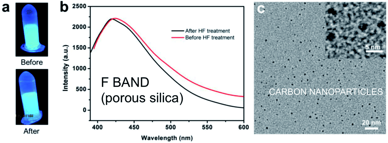 | ||
| Fig. 17 F-band like photoluminescence and carbon dot contamination of porous silica.286 Adapted with permission from H. Chen, Z. Zhen, W. Tang, T. Todd, Y. Chuang, L. Wang, Z. Pan and J. Xie, Theranostics, 2013, 3(9), 650–657. Copyright IvySpring. | ||
What this does demonstrate however, is that porous silica and oxidized porous silicon nanostructures can act as unintentional “nanoreactors” for carbon dot synthesis. Careful experimentation is required to check that F-band-like emission is not a result of carbon contamination of an initially hydrophobic and organophilic nanostructure. As pointed out many years ago, there is direct evidence of carbon contamination of hydride-terminated porous silicon from a variety of sources: extensive water rinsing used to remove HF residues;289 atmospheric and vacuum storage;149 plastic wafer and sample container outgassing.279 Low levels of carbon contamination are likely to generate F-band emission that is detectable, but of low PLQY. Intentional carbon impregnation of mesoporous silica (e.g. by glycerol) is now used by the carbon dot scientific community to generate high PLQY290 in the blue–green spectral range. It would be informative to search for carbon dots as well as silicon quantum dots in the now varied protocols for realizing ultrahigh F-band PLQY (see Table 7). It is also noteworthy that the carbon dot research community has similar issues with regards to unintentional fluorescent impurities.287,288 Without sufficient purification steps, molecular carbon-based chromophores can contribute the majority of the emission from bottom-up carbon dot formulations. Intentional introduction of both silicon and carbon dots into silica has led to white light emission (see Section 4.5), so optimizing PLQY for both S and F-bands can be of use, even if their origins are completely different.
4. PL applications
4.1. Sensing
Very soon after the demonstration of efficient visible photoluminescence from porous silicon47 it became apparent that PL output could be sensitive to a range of adsorbates.291 This has been the basis of many studies exploiting the photochemical properties of nanoscale silicon to attain sensors for gas and liquid analytes. Prior reviews include those of Sailor et al.,292 Gonzalez et al.293 and Ji et al.294 Chemical toxicants, pollutants and biomedical analytes have been the primary targets. Both PL quenching295–299 and enhancements (“photobrightening”) have been reported.300,301 The vast majority of sensors have utilized PL quenching, which in many cases is reversible, but irreversible quenching has also been considered for single-use sensors.Fig. 18 illustrates S-band sensing of various explosives with silicon nanocrystals embedded within a convenient paper substrate.
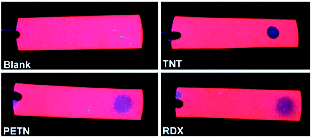 | ||
| Fig. 18 S-band sensing of explosives.314 Reproduced with permission from C. M. Gonzalez, M. Iqbal, M. Dasog, D. G. Piercey, R. Lockwood, T. M. Kiapotke and J. G. C. Veinot, Nanoscale, 2014. Copyright Royal Society of Chemistry. | ||
Quenching can be static (binding), dynamic (collisional), oxidation-induced or deposition-induced.302,303Table 9 and 10 collate the majority of sensing studies performed together with Limit of Detection (LOD) values and separate them into those that use the S-band (red–yellow PL) from the many recent studies exploiting the F-band (blue–green PL).
| Analyte class | Analyte | Sensing mode | LOD | Silicon nanostructure | References |
|---|---|---|---|---|---|
| Environmental contaminants and toxins | Aromatic hydrocarbons | PL quenching | 0.5 mM | pSi-hydride | (Fisher 1995)295 |
| Sulphur dioxide | PL quenching | 440 ppb | pSi-oxide | (Kelly 1996)304 | |
| Nitrogen dioxide | PL quenching and conductance | 5 ppm | pSi multilayer | (Baratto 2002)305 | |
| Alcohols | PL quenching | 40 ppm | pSi-undecanoate | (Holec 2002)306 | |
| Ethanol | PL quenching and PL decay rates | <620 ppm (vapour) | pSi- native oxide | (Dian 2007)307 | |
| Alcohols | PL quenching | 0.2 μM (vapour) | pSi-undecanoate | (Dian 2010)308 | |
| Ethanol | PL quenching | 380 ppm (vapour) | NP-hydride | (Zhang 2013)309 | |
| Heavy metals | Immunoassay | 10 nM | pSi-enzyme | (Syshchyk 2014)310 | |
| Copper | PL quenching | 1 μM | pSi-alkyl | (Hwang 2016)311 | |
| Aflatoxin | PL quenching | 2.5 pg mL−1 | pSi-Au-protein | (Myndrul 2017)312 | |
| Metal ion discrimination | PL quenching and peak shift | 10 μM | pSi-native oxide | (Jin 2019)303 | |
| Explosives | TNT, DNT | PL quenching | 1–2 ppb | pSi-hydride | (Content 2000)313 |
| DNB, DNT | PL quenching and PL decay rates | <50 μM | NP-oxide | (Germanenko 2001)314 | |
| DNT | PL quenching | 18.2 ng (solid) | NP-alkyl | (Gonzalez 2014)315 | |
| DNT | PL quenching | 6 ppb (vapour) | NP-alkyl | (Nguyen 2016)316 | |
| Medical analytes | Nitric oxide | PL quenching | 2 ppb | pSi-hydride | (Harper 1996)296 |
| Viral DNA | PL shift | 194 fM | pSi multilayer | (Chan 2000)317 | |
| Gram negative bacteria | PL shift | 1.7 μg | pSi multilayer | (Chan 2001)318 | |
| Urea | PL quenching | 30 μM | pSi and enzyme | (Chaudhari 2005)319 | |
| Ascorbic acid | PL quenching | 2 mM | pSi-oxide | (La Ferrara 2012)320 | |
| Intracellular Cu | PL quenching | 2.5 μM | pSi-carboxyl | (Xia 2013)321 | |
| AChE inhibitor | PL enhancement | 1.25 μg mL−1 | pSi-enzyme | (Saleem 2014)322 | |
| Human IgG | PL quenching | 500 fM | pSi-protein | (Cho 2015)323 | |
| Dopamine | Ratiometric PL quenching | 4 μM | pSi-silica | (Hollett 2019)302 |
| Analyte class | Analyte | Sensing mode | LOD | Silicon nanostructure | References |
|---|---|---|---|---|---|
| Environmental contaminants and toxins | Pesticides | PL enhancement | 7–200 ng L−1 | NP-enzyme | (Yi 2013)325 |
| Mercury | PL quenching | 50 nM | NP-amine | (Zhang 2014)326 | |
| Copper | PL quenching | 8 nM | NP-hydride | (Zhao 2014)327 | |
| Tetracyclines | 20–28 nM | NP-amine | (Lin 2015)328 | ||
| Chromium | PL quenching | 2.7 μM | NP-dendrimer | (Campos 2015)329 | |
| Copper | 0.5 μM | NP-oxide | (Liao 2016)330 | ||
| Sudan I | PL quenching | 39 nM | NP-hexadecylamine | (Jose 2016)331 | |
| Hypochlorite | PL quenching | 10 nM | NP-amine | (Guo 2016)332 | |
| Chromium, hydrogen, sulphide | PL quenching and restoration | 28 nM, 22 nM | NP-amine | (Zhu 2017)333 | |
| Crystal violet | PL quenching | 25 ng mL−1 | NP-amine | (Han 2018)334 | |
| Ethyl carbamate | RF-ELISA | 2.6 μg L−1 | NP-enzyme | (Luo 2018)335 | |
| Nitrophenol | PL quenching | 29 nM | NP-amine | (Han 2019)336 | |
| Explosives | TNT | PL quenching | 1 nM | NP-amine | (Ban 2015)337 |
| Medical analytes | Extracellular pH | PL quenching | pH 4–10 | NP-amine | (Feng 2014)338 |
| Dopamine | PL quenching | 0.3 nM | NP-amine | (Zhang 2015)339 | |
| Intracellular pH | Ratiometric | pH 4–10 | NP-amine | (Chu 2016)340 | |
| ALP | PL quenching | 1 U L−1 | NP-carboxyl | (Li 2018)341 | |
| Creatinine | PL quenching | 0.14 μM | NP-amine | (Meng 2019)342 | |
| Hemoglobin | PL quenching | 40 nM | NP-amine | (Li 2019)343 |
General advantages of fluorimetric (PL) sensing include low background signals and thereby high sensitivity, fast data acquisition and low cost. General challenges include sensor stability, specificity, repeatability, linearity, response and recovery times, and calibration. For Si-based sensors (Tables 9 and 10), approaches to improve specificity have included the immobilization of enzymes;319 ratiometric PL spectroscopy;302 combining PL quenching at a single wavelength with peak shifts;303 or decay time changes.307 With porous Si, multilayer microcavities offer multiparametric sensing.317 Recently, pSi-based biosensors have focussed on reflectance-based interferometry rather than photoluminescence-based analysis324 but as PLQY and more importantly, its stability, continues to improve, there could be a resurgence of interest in exploiting the S-band.
4.2. In vitro and in vivo imaging
Cellular and biomolecular imaging in vitro enables contactless studies of numerous physiological processes. Medical imaging facilitates noninvasive imaging of disease progression in vivo. These are critical tools in clinical diagnostics, physiology and cell biology.A significant volume of literature now exists on using photoluminescent silicon nanostructures for both in vitro and in vivo imaging. It has been the focus of a few prior reviews344–348 including a very recent one,349 so only a short overview will be given here.
The S-band emission has been used extensively in vitro as a “fluorescent label” in cell cultures.349–355 It is also increasingly being evaluated for in vivo use.357–366
The facile synthesis for achieving very high PLQY of F-band emission has led to a recent surge in its use as a label in vitro and there is now also a significant body of work on this.367–380 In contrast, in vivo usage of F-band emission is very rare.381
S-band emission can be used in vitro and in vivo, whereas F-band emission is generally restricted to in vitro use, because of high tissue absorption of both UV excitation wavelengths and blue–green emission wavelengths. Tissue has two “transmission windows” in the near infrared – 700–900 nm (“NIR 1”) and 1000–1700 nm (“NIR II”), where scattering and absorption of light is lower than adjacent wavelengths.382 The S-band emission of Si nanostructures normally falls within the NIR1 window. Interestingly, with degenerate doping of nanocrystals to shrink their bandgap, room temperature PL output in NIR II has also been achieved, but the PLQY was relatively low at about 2%.383 An ideal luminescent in vivo probe would have high PLQY with both excitation and emission occurring within these windows. Unfortunately, efficient PLQY of S-band emission necessitates short wavelength 300–450 nm excitation which limits the depth that can be imaged in vivo. For this reason there have been recent studies exploring two-photon excitation of the S-band384,385 where both excitation and emission target the NIR I window. Sailor and co-workers have recently shown the feasibility of this with 850 nm excitation under two photon microscopy (TPM) and 560–740 nm emission. Although the efficiency of this process with 60 nm pSiNPs was significantly lower than an established TPM molecular probe like rhodamine 6G, the porous silicon probe showed much better photostability, the ability to target tumours and carry drug payloads.366
Gooding and co-workers have also utilized two-photon excitation, in combination with in vitro fluorescence lifetime imaging, to excite F-band emission.386
A wide range of luminescent nanostructured materials are being assessed for in vivo medical imaging387 so I will summarize the perceived merits and challenges of using either the S-band or the F-band PL for biomedical imaging. There are 3 primary drivers for using S-band luminescence in Si nanostructures for in vivo imaging:
(a) Wavelength tunable and now very efficient luminescence output (see Table 7) within tissue window(s);
(b) Time-gated imaging that exploits the microsecond decay times to improve contrast;357,388,389
(c) Biodegradability356,390 combined with good in vivo biocompatibility in different body sites.391–393
Challenges for in vivo use of the S-band include low optical absorption coefficients, the relatively broad FWHM of PL, colloidal stability of the PL in body fluids, and one-photon excitation wavelengths lying outside the tissue windows.
When using the S-band for in vitro cell imaging the primary advantages are tunable emission, the low cytotoxicity of silicon nanoparticles394–400 and the flexible surface chemistry “toolbox” that has been realized (see Section 5.3).
For in vitro imaging exploiting the F-band emission, the primary advantages are very high PLQY (see Table 8), PL stability (less photobleaching and stable over a large pH range401) and narrower FWHM of PL than the S-band. Challenges for the F-band include the short excitation and emission wavelengths which overlap with tissue scattering and biological autofluorescence, and current uncertainties with regards to the origin of PL.
It should also be noted that whereas fluorescence labelling is a core technique used in in vitro cell biology, using luminescent agents in vivo is currently very much a developing research tool, rather than a mainstream clinical imaging modality. The latter point has relevance with regards to the likelihood of fast clinical translation of Si NP-based luminescence imaging and hence short-term impact. In this regard, the development of biomodal imaging probes, where photoluminescence imaging is combined with a more clinically established technique, has more potential for clinical translation. Unfortunately, silicon nanoparticles have low X-ray contrast compared to metals. Therefore more complex “nanoconstructs” are needed. There could be, for example, an opportunity for developing porous silicon with entrapped gas for a photoluminescent and biodegradable ultrasonic contrast agent. Table 11 provides examples from the literature – attention to date has been on accessing MRI rather than ultrasonic imaging.
| Photoluminescence emission | 2nd imaging mode | Silicon nanostructure | References |
|---|---|---|---|
| F-band (540 nm) | MRI | 3 nm NPs with iron oxides | (Sato 2011)402 |
| F-band (430 nm) | MRI | 3 nm NPs doped with iron | (Singh 2012)405 |
| S-band (750 nm) | MRI | 170 nm complex with 3 nm NPs and chelated Gd3+ | (Erogbogbo 2012)361 |
| S-band (500–800 nm) | MRI | pSi and iron oxide NPs | (Xia 2017)403 |
| F-band (460 nm) | MRI | 3.85 nm NPs with 19F ligands | (Li 2018)404 |
| F-band (400–510 nm) | MRI | 6.6 nm NPs doped with gadolinium | (Li 2018)381 |
| F-band | PET | 2.4 nm NPs with NIR dye and 64Cu radiolabel | (Singh 2020)406 |
4.3. Theranostics
Theranostic nanomedicine, where nanostructures simultaneously facilitate disease therapy and diagnosis, is currently dominated by drug delivery based therapies.407 In particular, the pre-clinical evaluation of pharmacokinetics and the target site and healthy organ accumulation of drugs.408 The potential of theranostics with nano-Si was initiated by the pioneering studies of Sailor and co-workers 357 who demonstrated in vivo imaging of S-band and organ targeting. The field has been very recently reviewed349 so only a short perspective is given here.Whilst for many therapies the luminescence provides only a means to track the nanostructures, the photosensitization of oxygen scales with PLQY.409 In contrast to photodynamic therapy, for photothermal therapy one wants to maximize non-radiative processes, so PL is unwanted. Thus luminescent Si nanostructures can themselves provide therapy (photosensitization409,410) or carry payloads that perform therapy (drugs, radioisotopes, metals349). Luminescent pSi is ideally suited to theranostics411,412 because of the much higher drug payloads achievable via filling the pore volume, compared to solid nanoparticles where the drug is attached only to the outer surfaces. At 80% porosity for example, drug payloads in pSi can exceed 50 wt% by melt loading techniques and the drug is itself nanostructured by entrapment within 5–50 nm mesopores. Control over pharmacokinetics is achieved via a combination of restricted diffusion and carrier biodegradability. Fig. 19 illustrates the multifunctionality of porous silicon nanoparticles (pSiNP).412
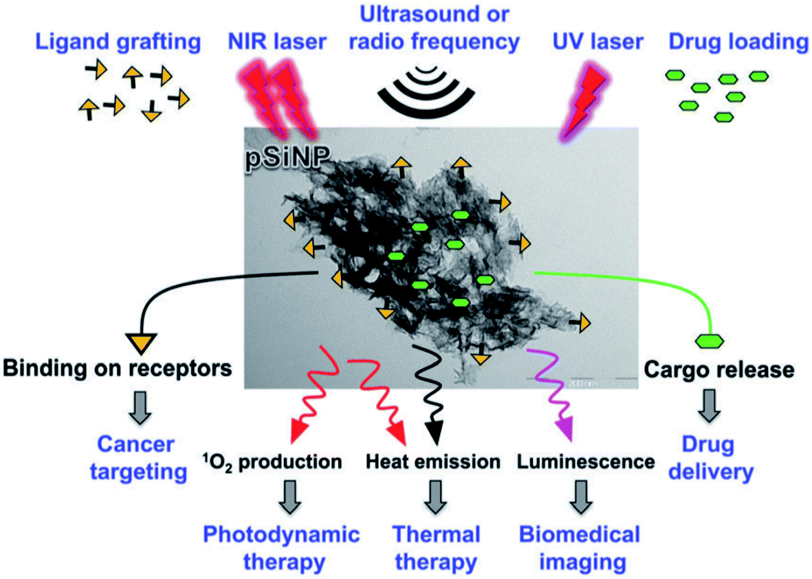 | ||
| Fig. 19 Theranostics with porous silicon nanoparticles.412 Reproduced with permission from V. Stojanovic, F. Cunin, J. O. Durand, M. Garcia and M. Gary-Bobo, J. Mater. Chem. B, 2016, 4, 7050–7059. Copyright Royal Society of Chemistry. | ||
4.4. Photovoltaics
A major limiting factor in the ultimate efficiency of silicon solar cells is the spectral mismatch between the energy distribution of the incident solar spectrum and the bandgap. An efficient photoluminescent material can act as a spectral converter to raise the efficiency of a solar cell by down-shifting (DS), quantum cutting (QC) or “upconversion” (UC) as shown schematically in Fig. 20.413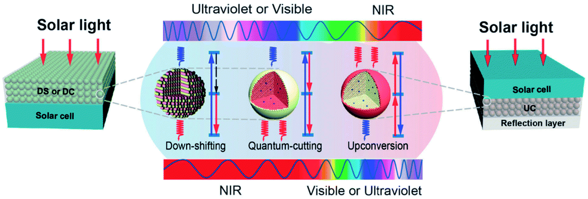 | ||
| Fig. 20 Classes of spectral converters.413 Reproduced with permission from C. X. Huang, S. Han, W. Huang and X. Liu, Chem. Soc. Rev., 2013, 42, 173–201. Copyright Royal Society of Chemistry. | ||
Visibly photoluminescent silicon can provide “down-shifters”414–420 or quantum cutters421–425 for traditional solar cells.
A second, recently emerged potential use is in “luminescent solar concentrators” (LSCs) for building integrated photovoltaics.426–428 Here, the large Stokes shift between strong UV absorption and S-band emission is of great benefit in minimizing light re-absorption over long distances. Solar concentrators are large plastic plates filled with photoluminescent material (commonly organic dyes) that redirect and concentrate solar energy to small photolvoltaic cells at their perimeter (see Fig. 21). A large fraction of the light can be effectively waveguided in the plastic sheet due to total internal reflections. The tunable bandgaps of silicon nanostructures offer design freedom with regards to aesthetics and optical performance. Challenges for silicon solar concentrator use include low absorptivity, scattering due to nanocrystal agglomeration, scalability of production and above all, cost.
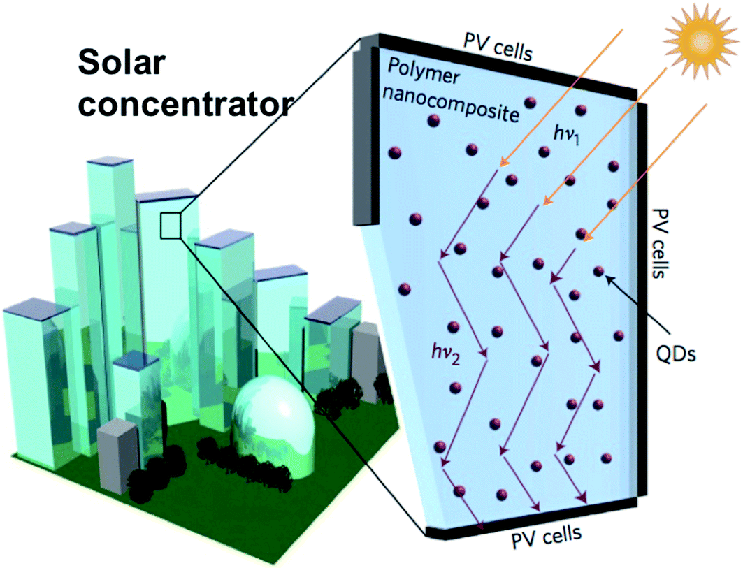 | ||
| Fig. 21 Luminescent solar concentrator using photoluminescent silicon nanocrystals.426 Reprinted with permission from F. Meinardi, S. Ehrenberg, L. Dhamo, F. Carulli, M. Mauri, F. Bruni, R. Simonutti, U. Kortshagen and S. Brovelli, Nature Photonics., 2017, 11, 177–186. Copyright 2017, Springer Nature. | ||
4.5. Colour converters for white LEDs
White light emitting LEDs of 5 lm W−1 brightness first became commercially available in 1996, and by 2010, brightness had already improved to the 150–250 lm W−1 range. The performance and cost of white LEDs are now competitive for general lighting, automotive, communication and medical uses.429 There are 3 methods for generating white light via an LED: (a) combining blue, green and red LEDs; (b) combing a UV LED with blue, green and red phosphors; and (c) using a blue LED to excite green or yellow and red phosphors. Fig. 22 illustrates methods (b) and (c). The latter approach (c) has received increasing use following the development of ultra-bright blue GaN LEDs in the 1990s.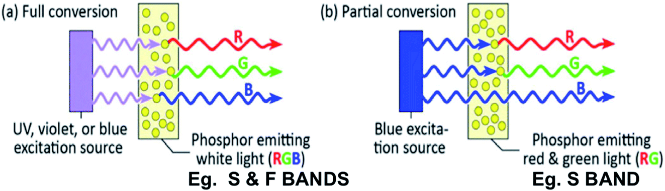 | ||
| Fig. 22 White light generation using red, green or blue photoluminescent materials.429 Adapted with permission from J. Cho, J. H. Park, J. K. Kim and E. F. Schubert, Laser Photonics. Rev., 2017, 11(2), 1600147. Copyright John Wiley & Sons. | ||
For general lighting the total power emitted, power efficiency and “whiteness” (colour temperature and rendering) are critical technical parameters. A 60 W incandescent tungsten light bulb, for example, currently has a luminous flux of 1000 lumins (lm) and a luminous efficiency of 17 lm W−1. The colour rendering index (CRI) is a quantitative measure of a light source’s ability to reproduce the colours of objects against natural or reference colours. Perfect performance is 100. Fluorescent lights typically have values in the range 50–98. LEDs are typically around 80. Colour correlated temperature (CCT) quantifies the temperature of an ideal blackbody radiating light of a colour comparable to the light source. Daylight (“cool”) white has a CCT values above 5000 K, neutral white 3000–5000 K, whilst incandescent (“warm”) white corresponds to a CCT value in the range 2500–3000 K.
In 2014 the start-up company Lumisands Inc, USA, reported the first use of visibly photoluminescent Si to generate “warm” white LEDs by method (b), and combined the use with other green and blue phosphors.430 The Si NPs were derived from porous silicon. Surprisingly high PLQY values for the S-band were estimated under blue (405 nm) excitation, especially since the authors reported their particles had “micron-size silicon cores with nanosize Si QD attached”. One would expect significant scattering and re-absorption of red emission with this type of structure. Colour rendering close to incandescent bulbs with a CCT ∼2800 K and CRI ∼95 were reported, without a value for luminous efficiency.
Broad band white PL has been reported from a number of silicon-containing nanostructures: heavily oxidized porous silicon,431 oxidized and carbon containing porous silicon,432,433 carbon doped silicon-rich silicon oxide434 and silicon and carbon co-implanted silica films.435 Ghosh et al.436 have also used method (b) but with white-light emitting Si nanocrystals containing material derived from rice husks (see Section 5.4) whose broad PL (230 nm FWHM) was possibly a combination of the S-band and F-band. In this regard, of particular relevance is the study where laser ablation of organosilica also produced white-emitting nanoparticles.437 Both silicon and carbon nanoparticles were discovered by TEM and are jointly attributed with white light generation. The carbon dots were revealed after HF removal of the silica phase, as used by Chen et al.286 and discussed in Section 3.6.
A study with commercial blue LEDs and porous silicon NPs embedded in an overlying polymer film demonstrated the flexibility of colour tuning by varying Si NP concentrations.438 Luminous efficiency was again not reported. For maximizing brightness, thin down-converting films should have low refractive indices to maximize light extraction efficiencies.128
The F-band has also been investigated for this application.439–441 Solution synthesis of nanoparticles was adapted to achieve broad yellow-green emissions centred at 540 nm under 410 nm excitation from a blue LED.439 The 43.5% EQE of the blue LED was reported to be lowered to 8% for the resulting white LED. A luminance efficiency value of 13 lm W−1 was provided together with CCT of 7982 K and a CRI of 82. In a second study by He’s group, luminescent nanorods achieved a similar luminance efficiency.440 In a third study, green emitting NPs with PLQY of 60%, derived from rice husks, were combined with blue and red emitting materials. Under 3 W UV LED excitation the composite film generated white light with a luminance efficiency of 75 lm W−1. Photostability of the green-emitting material was monitored over 1 month (720 hours) and PLQY dropped by 12%.
However, high reliability and a very long operating lifetime (50000–100000 hours) is one of the key features of LEDs that have led to their remarkable uptake in recent years. Successful inorganic color-converting phosphors like YAG:Ce have ultrahigh chemical stability that can withstand continuous ∼100 mW mm−2 radiance from a blue LED. Long-term photostability testing under intense blue/UV excitation is needed for Si nanostructures, as this might be a daunting challenge for this application area.
4.6. Nanothermometry
Measuring temperature with nanometer scale spatial resolution has potential widespread use in electronics, photonics and biomedicine but also a range of other niche areas.442 There are diverse methods but using luminescent probes of temperature are one of the most attractive, as they are non-invasive, contactless and easy to use.443 Most PL parameters are dependent to some extent on temperature: intensity (efficiency), spectral position, spectral shape, bandwidth, polarization and decay time. Which PL parameter(s) and which applications have the most potential for Si nanostructures? This topic is only starting to receive attention so it is difficult to gauge. Suggested specific applications to date range from tribology446 to cryosurgery.444Researchers at INSA, Lyon, were the first to realize the potential of S-band PL in this regard and they chose tribological studies of mechanical contacts as the target application area.445–450 Functionalized 4–8 nm porous Si NPs with S-band emission were studied in alkanes and alkenes from 293–393 K. As expected, with increasing temperature, red shifts of PL peak position were universally observed but data analysis revealed that shift magnitude also depended on solvent viscosity. They attributed this to Brownian motion causing energy transfer between nanoparticles of different size.450 A consequence is that temperature sensitivity will have a complex dependence on liquid viscosity, NP concentration, NP size distribution and NP passivation. A significant advance was therefore shown by Ferreira and Kortshagen’s groups451 who demonstrated that with better size control (2.0 ± 0.2 nm) of surface oxidized NPs, exciton migration effects were greatly reduced and the emission thermal dependence mainly follows the shrinkage of the bandgap. A single calibration then suffices for different media.
Use of the blue–green F-band in thermometry has also been reported.448,452 The low temperature solution synthesis route452 yielded very stable 480 nm emission with also very high 75% PLQY and monoexponential decay, but the PL origin is not established, and hence neither is the biodegradability of the luminescent entity (see Section 3.6). They chose to utilize decay times which linearly decreased from 23 ns at 0.5 °C to 8 ns at 60 °C, yielding a sensitivity of 0.24 ns °C−1 with a thermal resolution under 1 °C. Interestingly, when Ryabchikov and co-workers448 compared the thermal sensitivity of Si NCs with carbon NPs (produced by anodization of Si and SiC wafers, respectively) they found spectral shifts to be 3–4 times higher for the Si nanomaterial and of opposite sign to those of carbon dots (−0.18 vs. +0.05 meV K−1, respectively). Future comparative studies of the temperature responses of high PLQY F-band emissions from Si-based formulations and those of established “carbon dots” may thus provide further insight into the origin of the former.
The quantitative thermal sensitivity values reported to date for both S and F-bands are shown in Table 12. It is clear that, at least for the S-band for biomedical uses, the standard figures of merit are currently significantly lower than the highest values (1–5%/K) of other material systems.442 Nonetheless, with further improvements of surface passivation, size control and PLQY, the thermal sensitivity should improve, and this combined with having a thermometer system of tunable biodegradability, makes this an interesting area for further development.
| PL band and peak emission (nm) | PL parameter | Temperature range (K) | Thermal sensitivity | References |
|---|---|---|---|---|
| S (1.65 eV) | Decay time, peak position, intensity | 293–393, 293–373 | 0.1–0.3 μs K−1 (<0.75%/K), 0.18 meV K−1, −0.8%/K | (Ryabchikov 2012, 2013)445–447 |
| F (480) | Decay time | 273–333 | −0.24 ns K−1 | (Li 2013)452 |
| F (2.35 eV) | Peak position, bandwidth | 293–393 | +0.97 meV K−1, +1.2 meV K−1 | (Ryabchikov 2014)448 |
| S (630) | Peak position | 303–383 | −0.9 meV K−1 | (Hajjaji 2014)449 |
| S (1.7 eV) | Peak position | 303–390 | <0.052%/K | (Hamza 2015)450 |
| S (650) | Peak position | 13–480 | −0.04%/K | (Botas 2016)451 |
5. Summary and future perspectives
5.1. PL efficiency and passivation (stability)
Progress in improving PLQY of both the S-band (Table 7) and F-band (Table 8) over the last 30 years has been spectacular. Photostability of the S-band from derivatized silicon quantum dots is now competitive against many organic dyes with regards to biotagging. For applications like LED’s and photovoltaics where very long term stability is essential, further improvements in passivation seem mandatory. How do the effectiveness of surface passivation chemistries developed by the PV community for bulk Si compare with those used on silicon nanostructures? There are only a few studies that have estimated SRV values for 1 and 2D confinement in relatively large nanostructures that hence showed no S-band emission, as shown in Table 13.| Silicon nanostructure | Surface chemistry | Technique | SRV (cm s−1) | References |
|---|---|---|---|---|
| 2D Si nanolayer (90–200 nm) | Hydride | 1% HF treatment | 22.5 → 399 (10 K) air storage | (Coustel 2011)453 |
| 2D Si nanolayer (90–200 nm) | Alkyl groups | Hydrosilylation | 62 → 209 (10 K) air storage | (Coustel 2011)453 |
| Si nanowire (114, 224 nm diameter) | Thermal oxide (7–21 nm thick) | Diluted oxygen and forming gas at 960 °C | 20 | (Demichel 2010)454 |
| Si nanowire (25–125 nm diameter) | Thermal oxide (5–10 nm thick) | Diluted oxygen at 1000 °C | 10000–30000 |
(Grumstrup 2014)455 |
| Si nanowire (50–90 nm diameter) | a-Si (10 nm thick) | VLS deposition | 4500 | (Dan 2011)456 |
As for bulk silicon, hydride and organic monolayer passivation is metastable with SRV values rising with air storage. SRV values for nanowires can be remarkably high, reflecting perhaps challenges in avoiding defects along elongated nanostructures with highly curved interfaces.
5.2. Size control and wavelength tunability
If properties are size-dependent then size control and also metrology of nano-size distribution becomes critical.457,458 Control over size can be strived for during synthesis, or after synthesis, or a combination of the two. Some of the narrowest size distributions for as-synthesized silicon nanocrystals have been demonstrated with superlattice manipulation,459 gas phase laser ablation,460 plasma synthesis461 and micro-emulsion techniques.462,463 Some data are shown in Table 14. Various methods have also been applied to narrow size distributions of already fabricated luminescent silicon nanostructures (see Table 15). These include gas phase selection techniques,460–462,465,466 size selective precipitation,463 size exclusion chromatography199 and density gradient ultracentrifugation.196,468,469| References | (Tilley 2005)462, (Rosso-Vassic 2008)463 | (Patrone 2000)460 | (Tan 2011)265 | (Zacharias 2002171) | (Kothermann 2019)458 | (Gresback 2011)461 |
| Method | Reverse micelles | Laser ablation (gas phase) | Laser ablation (liquid phase) | Superlattice (reactive evaporation) | Superlattice (PECVD) | Plasma synthesis |
| Mean nanocrystal size (nm) | 1.6–1.8 | 1.8 | 2.37 | 3.4 | 3.7 | 5.0 |
| Size variation (SD nm) | 0.2 | 0.2 | 0.56 | 0.5 | 0.7 | 1.0 |
| PL emission band | F | S | F | S | S | S |
| References | (Littau 1993)199 | (Camata 1996)464 | (Mastronardi 2011)467 | (Miller 2012)468 | (Liu 2016)208 |
| Method | Size exclusion chromatography | Gas phase differential mobility | Size selective precipitation | Density gradient ultracentrifugation | Density gradient ultracentrifugation |
| Mean size (nm) | 7.5 | 2.8 | 1.61 | 3.60 | 2.81 |
| Size variation (SD nm) | 2.5 | 0.6 | 0.26 | 0.35 | 0.25 |
| PL emission band | S | — | S | S | S |
The S-band has been tuned over a wide spectral range but currently very high PLQY (>50%) is restricted to the 700–1000 nm red-near infrared region (see Table 7). The F-band has been tuned over a complementary spectral region with very high PLQY (>50%) in the 440–600 nm blue to yellow region (see Table 8).
5.3. Surface chemistry toolbox
The well-developed surface chemistry of bulk silicon470 was the platform from which many functionalization routes have been successfully applied to luminescent silicon nanostructures.471 The availability of metastable hydride surfaces has been both a help and a hindrance in this regard: it has facilitated the grafting of a wide range of organic capping ligands but 100% substitution seems virtually impossible due to steric hindrance issues. The resulting derivatized surfaces then have a mixed chemical nature with the desired Si–C bonding plus residual Si–H bonding. Oxidation is suppressed but not eliminated. Complex surface chemistries are more exploitable in ex vivo uses like sensing than in vivo imaging where clinical translation is needed for success. For applications where long term PL stability is of paramount importance, attention should focus on inorganic coatings that have a proven track record with regards to surface passivation of silicon (cf.Table 1). The challenge is to find scalable techniques that realize full surface coverage of nanostructures with low SRV values (cf.Table 13).5.4. Scalability and cost of luminescent silicon
Nanostructures are typically more much expensive than bulk materials and more difficult to manufacture at scale. Table 16 summarizes some reported throughputs for silicon nanocrystals. It is evident that the majority of these for luminescent nanocrystals lie in the range 0.1–10 g h−1 (i.e. less than 0.01 kg h−1). Whilst pilot plant production rates of about 1 kg h−1 have been reported, the nanocrystals were not small enough to be photoluminescent.| Silicon nanostructure | Luminescent? | Fabrication technique | Stated throughput (g h−1) | References |
|---|---|---|---|---|
| Nanocrystals, <5 nm | Yes (S-band) | Silane pyrolysis and stain etching | 0.02–0.2 | (Li 2003)472 |
| Nanocrystals, 4–9 nm | Yes (S-band) | Silane reduction | 0.1–1 | (Lacour 2007)473 |
| Nanocrystals, 100–500 nm | No | Silane reduction in pilot plant | 750 | (Hulser 2011)474 |
| Nanocrystals, (?) 2 nm | Yes (F-band) | Microwave assisted chemical synthesis | 0.6 | (Zhong 2013)245 |
| Nanocrystals, 2–10 and 50–120 nm | Yes (S-band) | Plasma decomposition of silane | 6 | (Dogan 2013)475 |
| Nanocrystals, (?) 4–9 nm | Yes (F-band) | Triethoxysilane reduction | 4–12 | (Pujari 2018)476 |
| Nanocrystals, 10–40 nm | No | Silane reduction | 22–200 | (Kunze 2019)477 |
Exciting progress has been made with silicon nanostructure synthesis by bottom-up high temperature techniques with molecular precursors and conversion synthesis with biogenic silica structures. Continuous belt-furnace production using “silicon accumulator plant” nanostructures478 is one very scalable technique for producing kilogrammes of biodegradable porous silicon. However, no efficient S-band emission has been reported to date from biogenic porous silicon. Where luminescent nanostructures have been achieved from plant material it has primarily been restricted to F-band emission441,479,480 and thus might be from carbonaceous material rather than any silicon nanoparticles also present. A significant goal is thus to achieve tunable S-band output of high PLQY from, for example, bamboo-derived silicon nanostructures. This would open a suite of new high volume and low cost uses (see next section). Dasog’s group have recently demonstrated that high S-band PLQY (∼50%) can be achieved via magnesiothermic reduction techniques.481 Synthetic sol–gel silica precursors were used. If this can be replicated with inexpensive biogenic silica feedstocks then the cost of visibly luminescent silicon should be significantly lowered in the future.
5.5. Novel applications
If the cost and scalability of luminescent nanosilicon can be lowered substantially then a range of further applications could emerge as commercially viable. In most cases, ultrahigh PLQY and much lower cost would need to be supplemented with another key attribute for that application. I mention a few examples here from the diverse fields of dentistry, cosmetics, environmental remediation, forensics and security:• Sunlight-driven photocatalyst (e.g. adsorbed toxicant degradation).
• Anti-ageing sunscreens (blue emitters and UV blockers).
• Dental “optical brightener” (tooth whitening formulations use blue emitters).
• Cosmetic skin hue converter (green-emitters used to mask red blemishes).
• Luminescent inks for banknotes (security features).
• Contrast agent in forensics (e.g. luminescent dusting powder).
6. Concluding comments
Remarkable progress has been made in raising the efficiency of visible emission from silicon-based quantum dots, superlattices and porous silicon over the last 30 years, with efficiencies of S-band red emission around 60–70% and green to blue F-band emission around 80–90% being the highest reported values. Surface chemistry plays a pivotal role in determining the efficiency and stability of emission. The widely tunable S-band arises from phonon-assisted exciton recombination within the silicon nanostructure. Emission in the F-band spectral range can have more than one origin, but carbon-based nanostructures and molecular chromophores are looking like the most likely origin of very efficient output. Some low temperature synthesis routes need to be revisited in this regard with more attention given to luminescent nanoparticle characterization and purification. Given the abundance of silica, low toxicity and biodegradability of luminescent silicon nanostructures compared to many other luminescent material nanosystems, their further development for a myriad of applications looks inevitable.Conflicts of interest
There are no conflicts of interest to declare.References
- A. Gupta and H. Wiggers, Free-standing silicon quantum dots: origin of red and blue emission, Nanotechnology, 2011, 22, 055707 CrossRef PubMed.
- J. I. Pankove, Optical processes in semiconductors, Dover Press, 1975 Search PubMed.
- J. R. Haynes and W. C. Westphal, Radiation resulting from recombination of holes and electrons in silicon, Phys. Rev., 1956, 101, 1676–1678 CrossRef CAS.
- J. D. Cuthbert, Recombination kinetics of excitonic molecules and free excitons in intrinsic silicon, Phys. Rev. B: Solid State, 1970, 1, 1552–1557 CrossRef.
- J. R. Haynes, Experimental observation of the excitonic molecule, Phys. Rev. Lett., 1966, 17(16), 860–862 CrossRef CAS.
- P. L. Gourley and J. P. Wolfe, Thermodynamics of excitonic molecules in silicon, Phys. Rev. B: Condens. Matter Mater. Phys., 1979, 20(8), 3319–3327 CrossRef CAS.
- M. L. W. Thewalt and W. G. McMullen, Green and near-infrared luminescence due to the biexcitons in unperturbed silicon, Phys. Rev. B: Condens. Matter Mater. Phys., 1984, 30(10), 6232–6234 CrossRef CAS.
- A. G. Steele, W. G. McMullan and M. L. W. Thewalt, Discovery of polyexcitons, Phys. Rev. Lett., 1987, 59(25), 2899–2902 CrossRef CAS PubMed.
- R. B. Hammond, T. C. McGill and J. W. Mayer, Temperature dependence of the electron-hole liquid luminescence in silicon, Phys. Rev. B: Solid State, 1976, 13(8), 3566–3575 CrossRef CAS.
- P. L. Gourley and J. P. Wolfe, Spatial condensation of strained confined excitons and excitonic molecules into an electron-hole liquid in silicon, Phys. Rev. Lett., 1978, 40(8), 526–530 CrossRef CAS.
- J. R. Haynes, Experimental proof of a new electronic complex in silicon, Phys. Rev. Lett., 1960, 4(7), 361–363 CrossRef CAS.
- R. C. Enck and A. Honig, Radiative spectra from shallow donor-acceptor electron transfer in silicon, Phys. Rev., 1969, 177(3), 1182–1193 CrossRef CAS.
- M. Tajima, T. Iwai, H. Toyota, S. Binetti and D. Macdonald, Fine structure due to donor-acceptor pair luminescence in compensated Si, Appl. Phys. Express, 2010, 3, 071301 CrossRef.
- M. Tajima, T. Iwai, H. Toyota, S. Binetti and D. Macdonald, Donor-acceptor pair luminescence in compensated Si for solar cells, J. Appl. Phys., 2011, 110, 043506 CrossRef.
- M. A. Tamor and J. P. Wolfe, Drift and diffusion of free excitons in Si, Phys. Rev. Lett., 1980, 44(25), 1703–1706 CrossRef CAS.
- P. J. Dean, J. R. Haynes and W. F. Flood, New radiative recombination processes involving neutral donors and acceptors in silicon and germanium, Phys. Rev., 1967, 161, 711–729 CrossRef CAS.
- M. Tajima, K. Tanaka, S. Dubois, J. Veirman, K. Nakagawa and A. Ogura, Photoluminescence due to impurity cluster bound exciton in highly doped and highly compensated silicon, Jpn. J. Appl. Phys., 2015, 54, 111304 CrossRef.
- J. Weber, W. Schmidt and R. Sauer, Localized exciton bound to an isoelectronic trap in silicon, Phys. Rev. B: Condens. Matter Mater. Phys., 1980, 21(6), 2401–2414 CrossRef CAS.
- N. A. Drozdov, A. A. Patrin and V. D. Tkatchev, Recombination radiation on dislocations in silicon, JETP Lett., 1976, 23(11), 597–599 Search PubMed.
- R. Sauer, J. Weber and J. Stolz, Dislocation-related photoluminescence in silicon, Appl. Phys. A: Solids Surf., 1985, 36, 1–13 CrossRef.
- H. Weman, B. Monemar, G. S. Oehrlein and S. J. Jeng, Strain-induced quantum confinement of carriers due to extended defects in silicon, Phys. Rev. B: Condens. Matter Mater. Phys., 1990, 42(5), 3109–3112 CrossRef CAS PubMed.
- K. Bothe, R. J. Falster and J. D. Murphy, Room temperature sub-bandgap photoluminescence from silicon containing oxide precipitates, Appl. Phys. Lett., 2012, 101, 032107 CrossRef.
- A. M. Stoneham, Non radiative transitions in semiconductors, Rep. Prog. Phys., 1981, 44, 1251–1295 CrossRef.
- A. Richter, S. W. Glunz, F. Werner, J. Schmidt and A. Cuevas, Improved quantitative description of Auger recombination in crystalline silicon, Phys. Rev. B: Condens. Matter Mater. Phys., 2012, 86, 165202 CrossRef.
- A. Hangleiter, Nonradiative recombination at deep defect levels in silicon: experiment, Phys. Rev. B: Condens. Matter Mater. Phys., 1987, 35(17), 9149–9161 CrossRef CAS PubMed.
- C. R. Helms and E. H. Poindexter, The silicon- silicon dioxide system: its microstructure and imperfections, Rep. Prog. Phys., 1994, 57(8), 791 CrossRef CAS.
- W. Bludau, A. Onton and W. Heinke, Temperature dependence of the bandgap of silicon, J. Appl. Phys., 1974, 45(4), 1846 CrossRef CAS.
- L. T. Canham, Room temperature photoluminescence from etched silicon surfaces: the effects of chemical pretreatments and gaseous ambients, J. Phys. Chem. Solids, 1986, 47(4), 363–373 CrossRef CAS.
- V. Alex, S. Finkbeiner and J. Weber, Temperature dependence of the indirect energy gap in crystalline silicon, J. Appl. Phys., 1996, 79, 6943 CrossRef CAS.
- A. G. Cullis, L. T. Canham and P. D. J. Calcott, The structural and luminescence properties of porous silicon, J. Appl. Phys., 1997, 82(3), 909–956 CrossRef CAS.
- G. Davies, The optical properties of luminescent centres in silicon, Phys. Rep., 1989, 176(3–4), 83–188 CrossRef CAS.
- L. T. Canham, M. R. Dyball, W. Y. Leong, M. R. Houlton, A. G. Cullis and P. W. Smith, Radiative recombination channels due to hydrogen in crystalline silicon, Mater. Sci. Eng., 1989, B4, 41–45 CrossRef CAS.
- R. S. Bonilla, B. Hoex, P. Hamer and P. R. Wilshaw, Dielectric surface passivation for silicon solar cells: a review, Phys. Status Solidi A, 2017, 214(7), 1700293 CrossRef.
- E. Yablonovitch, D. L. Allara, C. C. Chang, T. Gmitter and T. B. Bright, Unusually low surface recombination velocity on silicon and germanium surfaces, Phys. Rev. Lett., 1986, 57(2), 249–252 CrossRef CAS PubMed.
- Q. Sun, L. Melnikov, A. Mandelis and R. H. Pagliaro, Surface recombination velocity imaging of wet-cleaned silicon wafers using quantitative heterodyne lock-in carrierography, Appl. Phys. Lett., 2018, 112, 012105 CrossRef.
- E. J. Nemanik, P. T. Hurley, B. S. Brunschwig and N. S. Lewis, Chemical and electrical passivation of silicon (111) surfaces through functionalization with sterically hindered alkyl groups, J. Phys. Chem. B, 2006, 110, 41800–14808 Search PubMed.
- M. J. Kerr and A. Cuevas, Very low bulk and surface recombination in oxidiized silicon wafers, Semicond. Sci. Technol., 2002, 17, 35–38 CrossRef CAS.
- K. A. Collett, R. S. Bonilla, P. Hamer, G. Bourret-Sicotte, R. Lobo, T. Kho and P. R. Wilshaw, An enhanced alneal process to produce SRV <1 cm s−1 in 1 ohm cm n-type Si, Sol. Energy Mater. Sol. Cells, 2017, 173, 50–58 CrossRef CAS.
- Y. Wan, K. R. McIntosh, A. F. Thomson and A. Cuevas, Low surface recombination velocity by low absorption silicon nitride on c-Si, IEEE J. Photovolt., 2013, 3, 554–559 Search PubMed.
- B. Hoex, J. Schmidt, P. Pohl, M. C. M. van de Sanden and W. M. Kessels, Silicon surface passivation by atomic layer deposited Al2O3, J. Appl. Phys., 2008, 104, 044903 CrossRef.
- R. S. Bonilla, C. Reichel, M. Hermle and P. R. Wilshaw, Extremely low surface recombination in 1 ohm cm n-type monocrystalline silicon, Phys. Status Solidi RRL, 2017, 11, 1600307 CrossRef.
- W. J. Royea, A. Juang and N. S. Lewis, Preparation of air-stable low recombination velocity Si (111) surfaces through alkyl termination, Appl. Phys. Lett., 2000, 77(13), 1988–1990 CrossRef CAS.
- J. Bullock, D. Kiriya, N. Grant, A. Azcati, M. Hettick, T. Kho, P. Phang, H. C. Sio, D. Yan, D. Macdonald, M. A. Quevedo-Lopez, R. M. Wallace, A. Cuevas and A. Javey, Superacid passivation of crystalline Si surfaces, ACS Appl. Mater. Interfaces, 2016, 8, 24205–24211 CrossRef CAS PubMed.
- N. E. Grant, T. Niewelt, N. R. Wilson, E. C. Wheeler-Jones, J. Bullock, M. Al-Amin, M. C. Schubert, A. C. van Veen, A. Javey and A. D. Murphy, Superacid treated Si surfaces: extending the limit of carrier lifetime for photovoltaic applications, IEEE J. Photovolt. Appl., 2017, 7(6), 1574–1583 Search PubMed.
- J. Chen, K. Ge, C. Zhang, J. Guo, L. Wang, D. Song, F. Li, Z. Xu, Y. Xu and Y. Mai, Vacuum-free room temperature organic passivation of silicon: towards very low recombination of micro/nanotextured surface structures, ACS Appl. Mater. Interfaces, 2018, 10, 44890–44896 CrossRef CAS PubMed.
- Y. Yamashita, A. Asano, Y. Nishioka and H. Kobayashi, Dependence of interface states in the Si band gap on oxide atomic density and interfacial roughness, Phys. Rev. B: Condens. Matter Mater. Phys., 1999, 59(24), 15872–15881 CrossRef CAS.
- L. T. Canham, Silicon quantum wire array fabrication by electrochemical and chemical dissolution of wafers, Appl. Phys. Lett., 1990, 57(10), 1046–1048 CrossRef CAS.
- H. Takagi, H. Ogawa, Y. Yamazaki, A. Ishikazi and T. Nakagiri, Quantum size effects on photoluminescence in ultrafine Si particles, Appl. Phys. Lett., 1990, 56, 2379 CrossRef CAS.
- Y. Ding and J. Ni, Electronic structures of silicon nanoribbons, Appl. Phys. Lett., 2009, 95, 083115 CrossRef.
- Y. H. Tang, L. Z. Pei, Y. W. Chen and C. Guo, Self-assembled silicon nanotubes under supercritically hydrothermal conditions, Phys. Rev. Lett., 2005, 95, 116102 CrossRef CAS PubMed.
- H. Nakano, T. Mitsuoka, M. Harada, K. Horibuchi, H. Nozaki, N. Takahashi, T. Nonaka, Y. Seno and H. Nakamura, Soft synthesis of single-crystal silicon monolayer sheets, Angew. Chem., Int. Ed., 2006, 45, 6303–6306 CrossRef CAS PubMed.
- U. Kim, I. Kim, Y. Park, K. Y. Lee, S. Y. Yim, J. G. Park, H. G. Ahn, S. H. Park and H. J. Choi, Synthesis of Si Nanosheets by a Chemical Vapor Deposition Process and Their Blue Emissions, ACS Nano, 2011, 5(3), 2176–2181 CrossRef CAS PubMed.
- S. W. Kim, J. Lee, J. H. Sung, D. Seo, I. Kim, M. H. Jo, B. W. Kwon, W. K. Choi and H. J. Choi, Two-Dimensionally Grown Single-Crystal Silicon Nanosheets with Tunable Visible-Light Emissions, ACS Nano, 2014, 8(7), 6556–6562 CrossRef CAS PubMed.
- D. Karar, N. R. Banddyopadhyay, A. K. Pramanick, D. Achharya, G. Conibeer, N. Banerjee, O. E. Kusmartseva and M. Ray, Quasi-two-dimensional luminescent silicon nanosheets, J. Phys. Chem. C, 2018, 122, 18912–18921 CrossRef CAS.
- Y. Kanemitsu, K. Suzuki, M. Kondo and S. Kyushin, Luminescence properties of a cubic silicon cluster: octacubasilane, Phys. Rev. B: Condens. Matter Mater. Phys., 1995, 51, 10666 CrossRef CAS PubMed.
- Q. Wang, B. Xu, J. Sun, H. Liu, Z. Zhao, D. Yu, C. Fan and J. He, Direct band gap silicon allotropes, J. Am. Chem. Soc., 2014, 136, 9826–9829 CrossRef CAS PubMed.
- A. Kailer, Y. G. Gogotsi and K. G. Nickel, Phase transformations of silicon caused by contact loading, J. Appl. Phys., 1997, 81(7), 3057–3063 CrossRef CAS.
- A. J. Read, R. J. Needs, K. J. Nash, L. T. Canham, P. D. J. Calcott and A. Qteish, First priniciples calculations of the electronic properties of silicon quantum wires, Phys. Rev. Lett., 1992, 69(8), 1232–1235 CrossRef CAS PubMed.
- C. Delerue, G. Allan and M. Lannoo, Theoretical aspects of the luminescence of porous silicon, Phys. Rev. B: Condens. Matter Mater. Phys., 1993, 48(15), 11024 CrossRef CAS PubMed.
- M. S. Hybertsen and M. Needels, First-principles analysis of electronic states in silicon nanoscale quantum wires, Phys. Rev. B: Condens. Matter Mater. Phys., 1993, 48(7), 4608–4611 CrossRef CAS PubMed.
- B. Delley and E. F. Steigmeier, Size dependence of band gaps in silicon nanostructures, Appl. Phys. Lett., 1995, 67(16), 2370–2372 CrossRef CAS.
- S. Ke, K. Zhang and X. Xie, Electronic structures and optical absorption spectra of hydrogen-terminated Si quantum slabs, Phys. Rev. B: Condens. Matter Mater. Phys., 1997, 55(8), 5124–5128 CrossRef CAS.
- B. K. Agrawal and S. Agrawal, First principles study of one-dimensional quantum confined H-passivated ultrathin Si films, Appl. Phys. Lett., 2000, 77(19), 3039–3041 CrossRef CAS.
- L. Lin, Z. Li, J. Feng and Z. Zhang, Indirect to direct band gap transition in ultra-thin silicon films, Phys. Chem. Chem. Phys., 2013, 15, 6063–6067 RSC.
- J. B. Xia and K. W. Cheah, Quantum confinement effect in silicon quantum well layers, Phys. Rev. B: Condens. Matter Mater. Phys., 1997, 56(23), 14925–14928 CrossRef CAS.
- M. Nishida, Theoretical study of luminescence enhancement in oxidized Si (001) ultrathin films, Phys. Rev. B: Condens. Matter Mater. Phys., 1998, 58(11), 7103–7112 CrossRef CAS.
- M. Nishida, Theoretical study of luminescence degradation by oxidation in Si (001) and Si (111) ultrathin films: gap states induced by oxidation, Phys. Rev. B: Condens. Matter Mater. Phys., 1999, 66(12), 8902–8908 CrossRef.
- J. M. Wagner, K. Seino, F. Bechstedt, A. Dymiati, J. Mayer, R. Rolver, M. Forst, B. Berghoff, B. Spangenberg and H. Kurz, Electronic band gap of Si/SiO2 quantum wells: comparison of ab initio calculations and photoluminescence measurements, J. Vac. Sci. Technol., A, 2007, 25(6), 1500–1504 CrossRef CAS.
- S. Ossicini, A. Fasolino and F. Bernardini, Gap opening in ultrathin Si layers: role of confined and interface states, Phys. Rev. Lett., 1994, 72(7), 1044–1047 CrossRef CAS PubMed.
- A. J. Read, R. J. Needs, K. J. Nash, L. T. Canham, P. D. J. Calcott and A. Qteish, First priniciples calculations of the electronic properties of silicon quantum wires, Phys. Rev. Lett., 1992, 69(8), 1232–1235 CrossRef CAS PubMed.
- F. Buda, J. Kohanoff and M. Parrinello, Optical properties of porous silicon: a first principles study, Phys. Rev. Lett., 1992, 69(8), 1272–1275 CrossRef CAS PubMed.
- G. D. Sanders and Y. C. Chang, Optical properties of free-standing silicon quantum wires, Appl. Phys. Lett., 1992, 60(20), 2525–2527 CrossRef CAS.
- C. Y. Yeh, S. B. Zhang and A. Zunger, Identity of the light emitting states in porous silicon wires, Appl. Phys. Lett., 1993, 63(25), 3455–3457 CrossRef CAS.
- B. Delley and E. F. Steigmeier, Quantum confinement in Si nanocrystals, Phys. Rev. B: Condens. Matter Mater. Phys., 1993, 47(3), 1397–1400 CrossRef CAS PubMed.
- A. B. FilonovG, V. Petrov, V. A. Novikov and V. E. Borisenko, Orientation effect in electronic properties of silicon wires, Appl. Phys. Lett., 1995, 67(8), 1090–1091 CrossRef.
- S. Ossicini, C. M. Bertoni, M. Biagini, A. Lugli, G. Roma and O. Bisi, Optical properties of isolated and interacting silicon quantum wires, Thin Solid Films, 1997, 297, 154–162 CrossRef CAS.
- A. M. Saitta, F. Buda, G. Fiumara and P. V. Giaquinta, Ab initio molecular dynamics studies of electronic and optical properties of silicon quantum wires: orientational effects, Phys. Rev. B: Condens. Matter Mater. Phys., 1996, 53(3), 1446–1451 CrossRef CAS PubMed.
- X. Zianni and A. G. Nassiopoulu, Photoluminescence lifetimes of Si quantum wires, Phys. Rev. B: Condens. Matter Mater. Phys., 2002, 66, 205323 CrossRef.
- R. Q. Zhang, Y. Lifshitz, D. D. D. Ma, Y. L. Zhao, T. Frauenheim, S. T. Lee and S. Y. Tong, Structures and energetics of hydrogen terminated Si nanowire surfaces, J. Chem. Phys., 2005, 123, 144703 CrossRef CAS PubMed.
- T. Vo, A. J. Williamson and G. Galli, First principles simulations of the structural and electronic properties of silicon nanowires, Phys. Rev. B: Condens. Matter Mater. Phys., 2006, 74, 045116 CrossRef.
- D. Yao, G. Zhang and B. Li, A universal expression of band gap for silicon nanowires of different cross-section geometries, Nano Lett., 2008, 8(12), 4557–4561 CrossRef CAS PubMed.
- Z. Wu, J. B. Neaton and J. C. Grossman, Quantum confinement and electronic properties of tapered silicon nanowires, Phys. Rev. Lett., 2008, 100, 246804 CrossRef PubMed.
- K. Zhuo and M. Y. Chou, Surface passivation and orientation dependence in the electronic properties of silicon nanowires, J. Phys.: Condens. Matter, 2013, 25, 145501 CrossRef PubMed.
- N. Zonias, P. Lagoudakis and C. K. Skylaris, Large scale first principles and tight binding density functional calcuations on hydrogen passivated silicon nanorods, J. Phys.: Condens. Matter, 2013, 22, 025303 CrossRef PubMed.
- I. J. T. Jensen, A. G. Ulyashin and O. M. Lovvik, Direct to indirect bandgap transitions in 〈110〉 silicon nanowires, J. Appl. Phys., 2016, 119, 015702 CrossRef.
- M. Nolan, S. O. Callaghan, G. Fagas, J. C. Greer and T. Frauenheim, Silicon nanowire bandgap modification, Nano Lett., 2007, 7(1), 34–38 CrossRef CAS PubMed.
- M. Gao, S. You and Y. Wang, First principles study of silicon nanowires with different surfaces, Jpn. J. Appl. Phys., 2008, 47(4S), 3303–3309 CrossRef CAS.
- D. B. Migas and V. E. Borisenko, Effects of oxygen, fluorine and hydroxyl passivation on electronic properties of (001) oriented silicon nanowires, J. Appl. Phys., 2008, 104, 024314 CrossRef.
- K. Zhuo and M. Y. Chu, Surface passivation and orientation dependence in the electronic properties of silicon nanowires, J. Phys.: Condens. Matter, 2013, 25, 145501 CrossRef PubMed.
- I. Vasiliev, J. R. Chelikowsky and R. M. Martin, Surface oxidation effects on the optical properties of silicon nanocrystals, Phys. Rev. B: Condens. Matter Mater. Phys., 2002, 65, 121302 CrossRef.
- C. S. Garoufalis, A. D. Zdetsis and S. Grimme, High Level Ab Initio Calculations of the Optical Gap of Small Silicon Quantum Dots, Phys. Rev. Lett., 2001, 87(27), 276402 CrossRef CAS PubMed.
- J. See, P. Dolfus and S. Galdin, Comparison between a sp3d5 tight binding and an effective mass description of Si quantum dots, Phys. Rev. B: Condens. Matter Mater. Phys., 2002, 66, 193307 CrossRef.
- N. Tit, Z. H. Yamani, J. Graham and A. Ayesh, Effects of the passivating coating on the properties of silicon nanocrystals, Mater. Chem. Phys., 2010, 124, 927–935 CrossRef CAS.
- P. Hapala, K. Kusova, I. Pelant and P. Jelinek, Theoretical analysis of electronic band structure of 2–3 nm Si nanocrystals, Phys. Rev. B: Condens. Matter Mater. Phys., 2013, 87, 195420 CrossRef.
- A. Puzder, A. J. Williamson, J. C. Grossman and G. Galli, Surface control of optical properties in silicon nanoclusters, J. Chem. Phys., 2002, 117(14), 6721–6729 CrossRef CAS.
- Z. Zhou, L. Brus and R. Friesner, Electronic Structure and Luminescence of 1.1 and 1.4 nm Silicon Nanocrystals: Oxide Shell versus hydrogen Passivation, Nano Lett., 2003, 3(2), 163–167 CrossRef CAS.
- M. Luppi and S. Ossicini, Multiple Si
![[double bond, length as m-dash]](https://www.rsc.org/images/entities/char_e001.gif) O bonds at the silicon cluster surface, J. Appl. Phys., 2003, 94, 2130 CrossRef CAS.
O bonds at the silicon cluster surface, J. Appl. Phys., 2003, 94, 2130 CrossRef CAS. - G. Hadjisavvas and P. C. Kelires, Structure and energetics of Si nanocrystals embedded in a-SiO2, Phys. Rev. Lett., 2004, 93, 226104 CrossRef CAS PubMed.
- X. Chen, X. Pi and D. Yang, Bonding of Oxygen at the Oxide/Nanocrystal Interface of Oxidized Silicon Nanocrystals: An Ab Initio Study, J. Phys. Chem. C, 2010, 114, 8774–8781 CrossRef CAS.
- R. Wang, X. Pi and D. Yang, First-Principles Study on the Surface Chemistry of 1.4 nm Silicon Nanocrystals: Case of Hydrosilylation, J. Phys. Chem. C, 2012, 116, 19434–19443 CrossRef CAS.
- Z. Ni, X. Pi and D. Yang, Density functional theory study on a 1.4 nm silicon nanocrystal coated with carbon, RSC Adv., 2012, 2, 11227–11230 RSC.
- V. Kocevski, O. Eriksson and J. Rusz, Transition between direct and indirect band gap in silicon nanocrystals, Phys. Rev. B: Condens. Matter Mater. Phys., 2013, 87, 245401 CrossRef.
- P. Hapala, K. Kusova, I. Pelant and P. Jelinek, Theoretical analysis of electronic band structure of 2–3 nm Si nanocrystals, Phys. Rev. B: Condens. Matter Mater. Phys., 2013, 87, 195420 CrossRef.
- H. Li, Z. Wu, T. Zhou, A. Sellinger and M. T. Lusk, Tailoring the optical gap of silicon quantum dots without changing their size, Phys. Chem. Chem. Phys., 2014, 16, 19275–19281 RSC.
- T. Zhou, R. T. Anderson, H. Li, J. Bell, Y. Yang, B. P. Gorman, S. Pylypenko, M. T. Lusk and A. Sellinger, Bandgap Tuning of Silicon Quantum Dots by Surface Functionalization with Conjugated Organic Groups, Nano Lett., 2015, 15(6), 3657–3663 CrossRef CAS PubMed.
- V. Kocevski, Temperature dependence of radiative lifetime, optical and electronic properties of silicon nanocrystals capped with various organic ligands, J. Chem. Phys., 2018, 149, 054301 CrossRef CAS PubMed.
- M. Rohlfing and S. G. Loiue, Excitonic effects and the optical absorption spectrum of hydrogenated Si clusters, Phys. Rev. Lett., 1998, 80(15), 3320–3323 CrossRef CAS.
- O. Lehtonen and D. Sundholm, Density functional studies of excited states of silicon nanoclusters, Phys. Rev. B: Condens. Matter Mater. Phys., 2005, 72, 085424 CrossRef.
- M. Cruz, M. R. Beltran, C. Wang, J. Taguena-Martinez and Y. G. Rubo, Supercell approach to the properties of porous silicon, Phys. Rev. B: Condens. Matter Mater. Phys., 1999, 59(23), 15381–15387 CrossRef CAS.
- B. Sapoval, S. Russ and J. N. Chazalviel, Eigenstates in irregular quantum wells: application to porous silicon, J. Phys.: Condens. Matter, 1996, 8, 6235–6249 CrossRef CAS.
- F. A. Reboredo, A. Franceschetti and A. Zunger, Dark excitons due to direct Coulomb interactions in silicon quantum dots, Phys. Rev. B: Condens. Matter Mater. Phys., 2000, 61(19), 13073–13087 CrossRef CAS.
- D. Gabay, X. Wang, V. Lomakin, A. Boag, M. Jain and A. Natan, Size dependent electronic properties of silicon quantum dots – an analysis with hybrid, screened hybrid and local density functional theory, Comput. Phys. Commun., 2017, 221, 95–10 CrossRef CAS.
- T. Takagahara and T. Takeda, Theory of the quantum confinement effect on excitons in quantum dots of indirect gap materials, Phys. Rev. B: Condens. Matter Mater. Phys., 1992, 46(23), 15578–15581 CrossRef CAS PubMed.
- D. H. Feng, Z. Z. Xu, T. Q. Jia, X. X. Li and S. Q. Gong, Quantum size effects on exciton states in indirect gap quantum dots, Phys. Rev. B: Condens. Matter Mater. Phys., 2003, 68, 035334 CrossRef.
- C. Delerue, G. Allan and M. Lannoo, Electron-phonon coupling and optical transitions for indirect semiconductor nanocrystals, Phys. Rev. B: Condens. Matter Mater. Phys., 2001, 64, 193402 CrossRef.
- X. H. Peng, S. Ganti, A. Alizadeh, N. Bhate, K. K. Varanasi, S. K. Kumar and S. K. Nayak, Strain-engineered photoluminescence of silicon nanoclusters, Phys. Rev. B: Condens. Matter Mater. Phys., 2006, 74, 035339 CrossRef.
- X. H. Peng, A. Alizadeh, P. Sharma, S. K. Kumar and S. K. Nayak, First principles investigation of strain effects on the energy gaps in silicon nanoclusters, J. Phys.: Condens. Matter, 2007, 19, 266212 CrossRef PubMed.
- S. Z. Karazhanov, A. Davletova and A. Ulyashin, Strain induced modulation of band structure of silicon, J. Appl. Phys., 2008, 104, 024501 CrossRef.
- K. Kusova, P. Hapala, J. Valenta, P. Jelinek, O. Cibulka, L. Ondic and I. Pelant, Direct bandgap silicon: tensile strained silicon, Adv. Mater. Interfaces, 2014, 1, 1300042 CrossRef.
- S. Horiguchi, Conditions for a direct band gap in Si quantum wires, Superlattices Microstruct., 1998, 23(2), 355–364 CrossRef.
- T. Trupke, J. Zhao, A. Wang, R. Corkish and M. A. Green, Very efficient light emission from bulk crystalline silicon, Appl. Phys. Lett., 2003, 82(18), 2996–2998 CrossRef CAS.
- G. A. Crosby and J. N. Denas, Measurement of photoluminescence quantum yields. Review, J. Phys. Chem., 1971, 75(8), 991–1024 CrossRef CAS.
- T. S. Ahn, R. O. Al-Kasyi, A. M. Muller, K. M. Wentz and C. J. Bardeen, Self-absorption correction for solid-state photoluminescence quantum yields obtained from integrating sphere measurements, Rev. Sci. Instrum., 2007, 78, 086105 CrossRef.
- A. M. Brouwer, Standards for photoluminescence quantum yield measurements in solution (IUPAC Technical Report), Pure Appl. Chem., 2011, 83(12), 2213–2228 CAS.
- C. Wurth, M. Grabolle, J. Pauli, M. Spieles and U. Resh-Genger, Comparison of methods and achievable uncertainties for the relative and absolute measurements of photoluminescence quantum yields, Anal.Chem., 2011, 83(9), 3431–3439 CrossRef CAS PubMed.
- S. Leyre, E. Coutino-Gonzalez, J. J. Joos, J. Ryckaert, Y. Meuret, D. Poelman, P. F. Smet, G. Durinck, J. Hofkens, G. Deconinck and P. Hanselaer, Absolute determination of photoluminescence quantum efficiency using an integrating sphere setup, Rev. Sci. Instrum., 2014, 85, 123115 CrossRef CAS PubMed.
- J. Valenta, Determination of absolute quantum yields of luminescing nanomaterials over a broad spectral range: from the integrating sphere theory to the correct methodology, Nanosci. Methods, 2014, 3(1), 11–27 CrossRef CAS.
- Z. T. Kang, B. Arnold, C. J. Summers and B. K. Wagner, Synthesis of silicon quantum dot buried SiOx films with controlled luminescent properties for solid state lighting, Nanotechnology, 2006, 17, 4477–4482 CrossRef CAS.
- Y. Zhong, B. Song, X. Shen, D. Guo and Y. He, Fluorescein sodium ligand modified silicon nanoparticles produce ultrahigh fluorescence with robust pH- and photo-stability, Chem. Commun., 2019, 55, 365–368 RSC.
- Q. Li, T. Y. Luo, M. Zhou, H. Abroshan, J. Huang, H. J. Kim, N. L. Rosi, Z. Shao and R. Jin, Silicon nanoparticles with surface nitrogen: 90% quantum yield with narrow luminescence bandwidth and the ligand structure based energy law, ACS Nano, 2016, 10, 8385–8393 CrossRef CAS PubMed.
- Z. Yuan, T. Nakamura, S. Adachi and K. Matsuishi, Improvement of laser processing for colloidal silicon nanocrystal formation in a reactive solvent, J. Phys. Chem. C, 2017, 121, 8623–8629 CrossRef CAS.
- Z. Yang, G. B. de los Reyes, L. V. Titova, I. Sychugov, M. Dasog, J. Linnros, F. A. Hegmann and J. G. C. Veinot, Evolution of the Ultrafast Photoluminescence of Colloidal Silicon Nanocrystals with Changing Surface Chemistry, ACS Photonics, 2015, 2(5), 595–604 CrossRef CAS.
- A. Marinins, R. Z. Shafagh, W. van der Wijngaart, T. Haraldsson, J. Linnros and J. G. C. Veinot, Light-converting polymer/Si nanocrystal composites with stable 60–70% quantum efficiency and their glass laminates, ACS Appl. Mater. Interfaces, 2017, 9, 30267–30272 CrossRef CAS PubMed.
- F. Sangghaleh, I. Sychugov, Z. Yang, J. G. C. Veinot and J. Linnros, Near-Unity Internal Quantum Efficiency of Luminescent Silicon Nanocrystals with Ligand Passivation, ACS Nano, 2015, 9(7), 7097–7104 CrossRef CAS PubMed.
- D. Jurbergs, E. Rogojina, L. Mangoloni and U. Kortshagen, Silicon nanocrystals with ensemble quantum yields exceeding 60%, Appl. Phys. Lett., 2006, 88, 233116 CrossRef.
- J. Valenta, M. Greben, S. A. Dyakov, N. A. Gippius, D. Hiller, S. Gutsch and M. Zacharias, Nearly perfect near infrared luminescence efficiency of Si nanocrystals: a comprehensive quantum yield study employing the Purcell effect, Sci. Rep., 2019, 9, 11214 CrossRef CAS PubMed.
- J. Joo, T. Defforge, A. Loni, D. Kim, Z. Y. Li, M. J. Sailor, G. Gautier and L. T. Canham, Enhanced quantum yield of photoluminescent porous silicon prepared by supercritical drying, Appl. Phys. Lett., 2016, 108, 153111 CrossRef.
- B. Song, Y. Zhong, S. Wu, B. Chu, Y. Su and Y. He, One dimensional fluorescent silicon nanorods featuring ultrahigh photostability, favourable biocompatibility and excitation wavelength dependent emission spectra, J. Am. Chem. Soc., 2016, 138, 4824–4831 CrossRef CAS.
- B. J. Ryan, M. P. Hanrahan, Y. Wang, U. Ramesh, C. K. A. Nyamekye, R. D. Nelson, Z. Liu, C. Huang, B. Whitehead, J. Wang, L. T. Roling, E. A. Smith, A. J. Rosini and M. G. Panthani, Silicene, siloxene or silicane? Revealing the structural and optical properties of silicon nanosheets derived from calcium disilicide, Chem. Mater., 2020, 32(2), 795–804 CrossRef CAS.
- K. A. Gonchar, L. A. Osminkina, R. A. Galkin, M. B. Gongalsky, V. S. Marshov, V. Yu. Timoshenko, M. N. Kulmas, V. V. Solovyev, A. A. Kudryavtsev and V. A. Sivakov, Growth, Structure and Optical properties of Silicon Nanowires formed by Metal-Assisted Chemical Etching, J. Nanoelectron. Optoelectron., 2012, 7(6), 602–606 CrossRef CAS.
- X. Lu, C. M. Hessel, Y. Yu, T. D. Bogart and B. A. Korgel, Colloidal Luminescent Silicon Nanorods, Nano Lett., 2013, 13, 3101–3105 CrossRef CAS.
- A. R. Goni, L. R. Muniz, J. S. Reparaz, M. I. Alonso, M. Garriga, A. F. Lopeandia, J. Rodriguez-Viejo, J. Arbitol and R. Rurali, Using high pressure to unravel the mechanism of visible emission in amorphous Si/SiOx nanoparticles, Phys. Rev. B: Condens. Matter Mater. Phys., 2014, 89, 045428 CrossRef.
- R. Anthony and U. Kortshagen, Photoluminescence quantum yields of amorphous and crystalline silicon nanoparticles, Phys. Rev. B: Condens. Matter Mater. Phys., 2009, 80, 115407 CrossRef.
- A. Irrera, M. J. L. Faro, C. D’Andrea, A. A. Leonardi, P. Artoni, B. Fazio, R. A. Picca, N. Cioffi, S. Trusso, G. Franzo, P. Musumeci, F. Priolo and F. Iacona, Light emitting silicon nanowires obtained by metal-assisted chemical etching, Semicond. Sci. Technol., 2017, 32, 043004 CrossRef.
- E. C. Cho, M. A. Green, J. Xia, R. Corkish, P. Reece and M. Gal, Clear quantum-confined luminescence from crystalline silicon/SiO2 single quantum wells, Appl. Phys. Lett., 2004, 84(13), 2286–2288 CrossRef CAS.
- T. Helbich, A. Lyuleeva, T. Ludwig, L. M. Schwerf, T. F. Fassier, P. Lugli and B. Rieger, One-step synthesis of photoluminescent covalent polymeric nanocomposites from 2D silicon nanosheets, Adv.Funct.Mater., 2006, 26, 6711–6718 CrossRef.
- A. G. Cullis and L. T. Canham, Visible light emission due to quantum size effects in highly porous silicon, Nature, 1991, 353, 335–337 CrossRef CAS.
- M. V. Wolkin, J. Jorne, P. M. Fauchet, G. Allan and C. Delerue, Electronic States and Luminescence in Porous Silicon Quantum Dots: The Role of Oxygen, Phys. Rev. Lett., 1999, 82(1), 197–200 CrossRef CAS.
- L. T. Canham, M. R. Houlton, W. Y. Leong, C. Pickering and J. M. Keen, Atmospheric impregnation of porous silicon at room temperature, J. Appl. Phys., 1991, 70, 422–431 CrossRef CAS.
- J. C. Vial, A. Bsiesy, F. Gaspard, R. Herino, M. Ligeon, F. Muller, R. Romestain and R. F. Macfarlane, Mechanisms of visible-light emission from electro-oxidized porous silicon, Phys. Rev. B: Condens. Matter Mater. Phys., 1992, 45(24), 14171–14176 CrossRef CAS PubMed.
- R. Boukeherroub, D. D. M. Wayner, D. J. Lockwood and L. T. Canham, Passivated luminescent porous silicon, J. Electrochem. Soc., 2001, 148(9), H91–H97 CrossRef.
- H. Mizuno, H. Koyama and N. Koshida, Oxide-free blue photoluminescence form photochemically etched porous silicon, Appl. Phys. Lett., 1996, 69(25), 3779–3781 CrossRef CAS.
- Y. H. Xie, W. L. Wilson, F. M. Ross, J. A. Mucha, E. A. Fitzgerald, J. M. Macauley and T. D. Harris, Luminescence and structural study of porous silicon films, J. Appl. Phys., 1992, 71, 2403 CrossRef CAS.
- J. Linnros, N. Lalic, A. Galeckas and V. Grivackas, Analysis of the stretched exponential photoluminescence decay from nanometer-sized silicon crystals in SiO2, J. Appl. Phys., 1999, 86(11), 6128–6134 CrossRef CAS.
- L. Pavesi and M. Ceschini, Stretched exponential decay of the luminescence in porous silicon, Phys. Rev. B: Condens. Matter Mater. Phys., 1993, 48(23), 17625–17628 CrossRef CAS PubMed.
- B. Gelloz and N. Koshida, Mechanism of a remarkable enhancement in the light emission from nanocrystalline porous silicon annealed in high pressure water vapor, J. Appl. Phys., 2005, 98, 123509 CrossRef.
- Y. Takahashi, T. Furuta, Y. Ono, T. Ishiyama and M. Tabe, Photoluminescence from a silicon quantum well formed on separation by implanted oxygen substrate, Jpn. J. Appl. Phys., 1995, 34, 950–954 CrossRef CAS.
- P. N. Saeta and A. C. Gallagher, Visible luminescence from single crystal silicon quantum wells, Appl. Phys. Lett., 1995, 77(9), 4639–4641 CAS.
- P. N. Saeta and A. C. Gallagher, Photoluminescence properties of silicon quantum well layers, Phys. Rev. B: Condens. Matter Mater. Phys., 1997, 55(7), 4563–4574 CrossRef CAS.
- S. Okamoto and Y. Kanemitsu, Quantum confinement and interface effects on photoluminescence from silicon quantum wells, Solid State Commun., 1997, 103(10), 573–576 CrossRef CAS.
- N. Pauc, V. Calvo, J. Eymery, F. Fournel and N. Magnea, Photoluminescence of nanometric single silicon quantum wells, Opt. Mater., 2005, 27, 1000–1003 CrossRef CAS.
- E. C. Cho, M. A. Green, J. Xia, R. Corkish, P. Reece, M. Gal and S. H. Lee, Photoluminescence in crystalline silicon quantum wells, J. Appl. Phys., 2007, 101, 024321 CrossRef.
- X. Zhu, J. Lu, Y. Gao, S. Yuan, N. Zhou, M. Xie, Z. Zheng and Y. Zhao, Strong photoluminescence from ultrathin silicon (110) quantum wells at room temperature, Jpn. J. Appl. Phys., 2017, 56, 020305 CrossRef.
- Z. H. Lu, D. J. Lockwood and J. M. Baribeau, Quantum confinement and light emission in SiO2/Si superlattices, Nature, 1995, 378, 258–260 CrossRef CAS.
- D. J. Lockwood, Z. H. Lu and J. M. Baribeau, Quantum confined luminescence in Si/SiO2 superlattices, Phys. Rev. Lett., 1996, 76(3), 539–541 CrossRef CAS PubMed.
- S. V. Novikov, J. Sinnkonen, O. Kilpela and S. V. Gastev, Visible luminescence from Si/SiO2 superlattices, J. Vac. Sci. Technol., B: Microelectron. Nanometer Struct.--Process., Meas., Phenom., 1997, 15(4), 1471–1473 CrossRef CAS.
- P. Photopoulos, A. G. Nassiopoulou, D. N. Kouvatsos and A. Travios, Photoluminescence from nanocrystalline silicon in Si/SiO2 superlattices, Appl. Phys. Lett., 2000, 76(24), 3588–3590 CrossRef CAS.
- V. Vinciguerra, G. Franzo, F. Priolo, F. Iacona and C. Spinella, Quantum confinement and recombination dynamics in silicon nanocrystals embedded in Si/SiO2 superlattices, J. Appl. Phys., 2000, 87(11), 8165–8173 CrossRef CAS.
- Y. Kanemitsu, Y. Fukenishi, M. Iiboshi and S. Okamoto, Visible luminescence from Si/SiO2 quantum wells and dots: confinement and localization of excitons, Physica E: Low-dimensional Systems and Nanostructures, 2000, 7, 456–460 CrossRef CAS.
- F. Gourbilleau, X. Portier, C. Ternon, P. Voivenei, R. Madelon and R. Rizk, Si-rich/SiO2 nanostructured multilayer’s by reactive magnetron sputtering, Appl. Phys. Lett., 2001, 78(20), 3058–3060 CrossRef CAS.
- M. Zacharias, J. Heitmann, R. Scholz, U. Kahler, M. Schmidt and J. Blasing, Size-controlled highly luminescent silicon nanocrystals: A SiO/SiO2 Superlattice approach, Appl. Phys. Lett., 2002, 80(4), 661–663 CrossRef CAS.
- F. A. D’Avitaya, L. Vervoort, F. Bassani, S. Ossicini, A. Fasolino and F. Bernardini, Light emission at room temperature from Si/CaF2 multilayers, Europhys. Lett., 1995, 31(1), 25–30 CrossRef.
- L. Vervoort, F. Bassani, I. Mihalcescu, J. C. Vial and F. Arnaud D’Avitaya, Efficient visible light emission from Si/CaF2(111) heterostructures grown by molecular beam epitaxy, Phys. Status Solidi B, 1995, 190, 123–127 CrossRef CAS.
- M. Watanabe, F. IIzuka and M. Asada, Visible light emission from nanocrystalline silicon embedded in CaF2 layers on Si (111), IEEE Trans. Electron Devices, 1996, E79-C, 1562–1567 Search PubMed.
- J. Heitmann, F. Muller, L. Yi, M. Zacharias, D. Kovalev and F. Eichhorn, Excitons in Si nanocrystals: Confinement and migration effects, Phys. Rev. B: Condens. Matter Mater. Phys., 2004, 69, 195309 CrossRef.
- J. Valenta, M. Greben, S. A. Dyakov, N. A. Gippius, S. Gutsch, D. Hiller and M. Zacharias, Effects of Inter-nanocrystal distance on luminescence quantum yield in ensembles of Si nanocrystals, Appl. Phys. Lett., 2014, 105, 243107 CrossRef.
- H. Namatsu, M. Nagasse, K. Kurihara, K. Iwadate, T. Furuta and K. Murase, Fabrication of sub-10 nm silicon lines with minimum fluctuation, J. Vac. Sci. Technol., B: Microelectron. Nanometer Struct.--Process., Meas., Phenom., 1995, 13(4), 1473–1476 CrossRef CAS.
- A. G. Nassiopoulos, S. Grigoropoulos and E. Gogolides, Visible luminescence from 1-dimensional and 2-dimensional silicon structures produced by conventional lithographic and reactive ion etching techniques, Appl. Phys. Lett., 1995, 66, 1114 CrossRef CAS.
- S. H. Zaidi and S. R. J. Brueck, Optical properties of nanoscale, one-dimensional silicon grating structures, J. Appl. Phys., 1996, 80(12), 6997–7007 CrossRef CAS.
- M. Gotza, M. Dutoit and M. Ilegems, Fabrication and photoluminescence investigation of silicon nanowires on silicon-on-insulator material, J. Vac. Sci. Technol., B: Microelectron. Nanometer Struct.--Process., Meas., Phenom., 1998, 16(2), 582 CrossRef CAS.
- D. P. Yu, Z. G. Bai, J. J. Wang, Y. H. Zou, W. Qian, J. S. Fu, H. Z. Zhang, Y. Ding, G. C. Xiong, L. P. You, J. Xu and S. Q. Feng, Direct evidence of quantum confinement from the size dependence of the photoluminescence of silicon quantum wires, Phys. Rev. B: Condens. Matter Mater. Phys., 1999, 59(4), R2898–R2501 CrossRef.
- A. R. Guichard, D. N. Barsic, S. Sharma, T. I. Kamins and M. L. Brongersma, Tunable light emission from quantum-confined excitons in TiSi2- catalyzed silicon nanowires, Nano Lett., 2006, 6(9), 2140–2144 CrossRef CAS PubMed.
- V. A. Sivakov, F. Voigt, A. Berger, G. Bauer and S. H. Christiansen, Roughness of silicon nanowire sidewalls and room temperature photoluminescence, Phys. Rev. B: Condens. Matter Mater. Phys., 2010, 82, 125446 CrossRef.
- V. Le Borgne, M. Agati, S. Boninelli, P. Castrucci, M. de Crescenzi, R. Dolbec and M. Y. A. E. Khakani, Structural and photoluminescence properties of silicon nanowires extracted by means of a centrifugation process from plasma torch synthesized silicon nanopowder, Nanotechnology, 2017, 28, 285702 CrossRef PubMed.
- L. Mangolini, Synthesis, properties and applications of silicon nanocrystals, J. Vac. Sci. Technol., B: Nanotechnol. Microelectron.: Mater., Process., Meas., Phenom., 2013, 31(2), 020801 Search PubMed.
- C. Huan and S. S. Qing, Silicon nanoparticles: Preparation, properties, and applications, Chin. Phys. B, 2014, 23(8), 088102 CrossRef.
- X. Cheng, S. B. Lowe, P. J. Reece and J. J. Gooding, Colloidal silicon quantum dots: from preparation to the modification of self-assembled monolayers (SAMs) for bio-applications, Chem. Soc. Rev., 2014, 43, 2680–2700 RSC.
- Y. Yu, G. Fan, A. Fermi, R. Mazzaro, V. Morandi, P. Ceroni, D. M. Smilgies and B. A. Korgel, Size-dependent photoluminescence efficiency of silicon nanocrystal quantum dots, J. Phys. Chem. C, 2017, 121, 23240–23248 CrossRef CAS.
- C. Garcia, B. Garrido, P. Pellegrino, R. Ferre, J. A. Moreno, L. Pavesi, M. Cazanelli and J. R. Morante, Size dependence of lifetime and absorption cross section of Si nanocrystals embedded in SiO2, Appl. Phys. Lett., 2003, 82, 1595 CrossRef CAS.
- C. Delerue, G. Allan, C. Reynaud, O. Guillard, G. Ledoux and F. Huisken, Multiexponential photoluminescence decay in indirect gap semiconductor nanocrystals, Phys. Rev. B: Condens. Matter Mater. Phys., 2006, 73, 235318 CrossRef.
- M. Greben, P. Khoroshyy, X. Liu, X. Pi and J. Valenta, Fully radiative relaxation of silicon nanocrystals in colloidal ensemble revealed by advance treatment of decay kinetics, J. Appl. Phys., 2017, 122, 034304 CrossRef.
- B. Gelloz, F. B. Juangsa, T. Nozaki, K. Asaka, N. Koshida and L. Jin, Si/SiO2 core/shell photoluminescent silicon nanocrystals and porous silicon powders with high quantum yield, long lifetime and good stability, Front. Phys., 2019, 7, 47 CrossRef.
- K. Furuta, M. Fujii, H. Sugimoto and K. Imakita, Energy Transfer in Silicon Nanocrystal Solids Made from All-Inorganic Colloidal Silicon Nanocrystals, J. Phys. Chem. Lett., 2015, 6, 2761–2766 CrossRef CAS PubMed.
- K. Potrick, T. Schmidt, S. Bublitz, Chr. Muhlig, W. Paa and F. Huisken, Determination of the photoluminescence quantum efficiency of silicon nanocrystals by laser-induced deflection, Appl. Phys. Lett., 2011, 98, 083111 CrossRef.
- R. J. Walters, J. Kalkman, A. Polman, H. A. Atwater and M. J. A. de Dood, Photoluminescence quantum efficiency of dense silicon nanocrystals ensembles in SiO2, Phys. Rev. B: Condens. Matter Mater. Phys., 2006, 73, 132302 CrossRef.
- M. L. Mastronardi, F. Maier-Flag, D. Faulkner, E. J. Henderson, C. Kubel, U. Lemmer and G. A. Ozin, Size-dependent absolute quantum yields for size-separated colloidally-stable silicon nanocrystals, Nano Lett., 2011, 12, 337–342 CrossRef PubMed.
- M. Zacharias, L. Tsybeskov, K. D. Hirschman, P. M. Fauchet, J. Blasing, P. Kohlert and P. Veit, Nanocrystalline silicon superlattices: fabrication and characterization, J. Non-Cryst. Solids, 1998, 227–230, 1132–1136 CrossRef CAS.
- L. E. Brus, P. F. Szajowski, W. L. Wilson, T. D. Harris, S. Schuppler and P. H. Citrin, Electronic Spectroscopy and Photophysics of Si Nanocrystals: Relationship to Bulk c-Si and Porous Si, J. Am. Chem. Soc., 1995, 117, 2915–2922 CrossRef CAS.
- K. A. Littau, A. J. Muller, P. J. Szawoski, A. R. Kortan and L. Brus, A luminescent silicon nanocrystal colloid via a high temperature aerosol reaction, J. Phys. Chem., 1993, 97, 1224–1230 CrossRef CAS.
- G. Ledoux, O. Guillois, D. Porterat, C. Reynaud, F. Huisken, B. Kohn and V. Paillard, Photoluminescence properties of silicon nanocrystals as a function of their size, Phys. Rev. B: Condens. Matter Mater. Phys., 2000, 62(23), 15942–15951 CrossRef CAS.
- S. Takeoka, M. Fujii and S. Hayashi, Size-dependent photoluminescence from surface-oxidized Si nanocrystals in a weak confinement regime, Phys. Rev. B: Condens. Matter Mater. Phys., 2000, 62, 16820–16825 CrossRef CAS.
- M. I. Alonso, I. C. Marcus, M. Garriga, A. R. Goni, J. Jedrzejewski and I. Balberg, Evidence of quantum confinement effects on interband optical transitions in Si nanocrystals, Phys. Rev. B: Condens. Matter Mater. Phys., 2010, 82, 045302 CrossRef.
- M. L. Brongersma, A. Polman, K. S. Min, E. Boer, T. Tambo and H. A. Atwater, Tuning the emission wavelength of Si nanocrystals in SiO2 by oxidation, Appl. Phys. Lett., 1998, 72(20), 2577–2579 CrossRef CAS.
- F. Iacona, G. Franzo and C. Spinella, Correlation between luminescence and structural properties of Si nanocrystals, J. Appl. Phys., 2000, 87(5), 1295–1303 CrossRef CAS.
- G. Polisski, H. Heckler, D. Kovalev, M. Schwartzkopff and F. Koch, Luminescence of porous silicon in a weak confinement regime, Appl. Phys. Lett., 1998, 73(8), 1107–1119 CrossRef CAS.
- J. Von Behren, T. van Buuren, M. Zacharias, E. H. Chimowitz and P. M. Fauchet, Quantum confinement in nanoscale silicon: the correlation of size with bandgap and luminescence, Solid State Commun., 1998, 105(5), 317–322 CrossRef CAS.
- J. Choi, N. S. Wang and V. Reipa, Photoassisted Tuning of Silicon Nanocrystal Photoluminescence, Langmuir, 2007, 23, 3388–3394 CrossRef CAS PubMed.
- X. Liu, Y. Zhang, T. Yu, X. Qiao, R. Gresback, X. Pi and D. Yang, Optimum quantum yield of the light emission from 2 to 10 nm hydrosilylated silicon quantum dots, Part. Part. Syst. Charact., 2016, 33(1), 44–52 CrossRef CAS.
- A. M. P. Botas, R. J. Anthony, J. Wu, D. J. Rowe, N. J. O. Silva, U. Kortshagen, R. N. Pereira and R. A. S. Ferreira, Influence of the surface termination on the light emission of crystalline silicon nanoparticles, Nanotechnology, 2016, 27, 325703 CrossRef PubMed.
- G. M. Carroll, R. Limpens and N. R. Neale, Tuning confinement in colloidal silicon nanocrystals with saturated surface ligands, Nano.Lett., 2018, 18(5), 3118–3124 CrossRef CAS PubMed.
- A. Angi, R. Sinelnikov, H. H. Heenen, A. Meldrum, J. G. C. Veinot, D. Azulay, I. Balberg, O. Millo and B. Rieger, The influence of conjugated alkylnyl (aryl) surface groups on the optical properties of silicon nanocrystals: photoluminescence through in-gap states, Nanotechnology, 2018, 29, 355705 CrossRef PubMed.
- M. Dasog, G. B. De los Reyes, L. V. Titova, F. A. Hegmann and J. G. C. Veinot, Size vs. Surface: Tuning the photoluminescence for Freestanding Silicon Nanocrystals Across the Visible Spectrum via Surface Groups, ACS Nano, 2014, 8(9), 9636–9648 CrossRef CAS PubMed.
- M. Dasog, K. Bader and J. G. C. Veinot, Influence of halides on the optical properties of silicon quantum dots, Chem. Mater., 2015, 27, 1153–1156 CrossRef CAS.
- P. D. J. Calcott, K. J. Nash, L. T. Canham, M. J. Kane and D. Brumhead, Identification of radiative transitions in highly porous silicon, J. Phys.: Condens. Matter, 1993, 5, L91–L98 CrossRef CAS.
- P. D. J. Calcott, K. J. Nash, L. T. Canham, M. J. Kane and D. Brumhead, Spectroscopic identification of the luminescence mechanism of highly porous silicon, J. Lumin., 1995, 57, 257–269 CrossRef.
- M. Rosenbauer, M. Stutzmann, S. Finkbeiner, J. Weber and E. Bustaret, Resonantly excited photoluminescence spectra of porous silicon, Phys. Rev. B: Condens. Matter Mater. Phys., 1995, 51(16), 10539–10547 CrossRef CAS PubMed.
- M. Rosenbauer, M. Stutzmann, S. Finkbeiner, J. Weber and E. Bustaret, Reply to “Comment on Resonantly excited photoluminescence spectra of porous silicon”, Phys. Rev. B: Condens. Matter Mater. Phys., 1997, 55(15), 10117–10118 CrossRef CAS.
- T. Suemoto and A. Saito, Comment on “Resonantly excited photoluminescence spectra of porous silicon”, Phys. Rev. B: Condens. Matter Mater. Phys., 1997, 55(15), 10115–10116 CrossRef CAS.
- Y. Kanemitsu and S. Okamato, Resonantly excited photoluminescence from porous silicon: effects of surface oxidation on resonant luminescence spectra, Phys. Rev. B: Condens. Matter Mater. Phys., 1997, 56(4), R1696–R1699 CrossRef CAS.
- Y. Kanemitsu and S. Okamato, Phonon structures and Stokes shift in resonantly excited luminescence of silicon nanocrystals, Phys. Rev. B: Condens. Matter Mater. Phys., 1998, 58, 9652 CrossRef CAS.
- J. L. Gole and S. M. Prokes, Resonantly excited photoluminescence from porous silicon and the question of bulk phonon replicates, Phys. Rev. B: Condens. Matter Mater. Phys., 1998, 58(8), 4761–4770 CrossRef CAS.
- H. Heckler, D. Kovalev, G. Polisski, N. N. Zinovev and F. Koch, Magneto-optical effects in photoluminescence of Si nanocrystals, Phys. Rev. B: Condens. Matter Mater. Phys., 1999, 60(11), 7718–7721 CrossRef CAS.
- G. F. Grom, D. J. Lockwood, J. P. McCaffrey, H. J. Labbe, P. M. Fauchet, B. White Jr, J. Diener, D. Kovalev, F. Koch and L. Tsybeskov, Ordering and self-organization in nanocrystalline silicon, Nature, 2000, 407, 358–361 CrossRef CAS PubMed.
- J. Heitman, F. Muller, L. Yi, M. Zacharias, D. Kovalev and F. Eichhorn, Excitons in silicon nanocrystals: confinement and migration effects, Phys. Rev. B: Condens. Matter Mater. Phys., 2004, 69, 195309 CrossRef.
- Y. Kanemitsu, H. Sato, S. Nihonyanage and Y. Hirai, Efficient radiative recombination of indirect excitons in silicon nanowires, Phys. Status Solidi A, 2002, 190, 755–758 CrossRef CAS.
- Y. Kanemitsu and S. Okamoto, Photoluminescence from Si/SiO2 single quantum wells by selective excitation, Phys. Rev. B: Condens. Matter Mater. Phys., 1997, 56, 15561 CrossRef.
- U. Kahler and H. Hofmeister, Size evolution and photoluminescence of silicon nanocrystallites in evaporated SiOx thin films upon thermal processing, Appl. Phys. A: Mater. Sci. Process., 2002, 74, 13–17 CrossRef CAS.
- D. Kovalev, H. Heckler, M. Ben-Chorin, G. Polisski, M. Schwartzkopf and F. Koch, Breakdown of the k-conservation rule in Si nanocrystals, Phys. Rev. Lett., 1998, 81(13), 2803–2806 CrossRef CAS.
- Y. Kanemitsu and S. Okamoto, Optical properties of hydrogen terminated silicon nanocrystals, Solid-State Electron., 1998, 42(7–8), 1315–1318 CrossRef CAS.
- B. Goller, S. Polisski, H. Wiggers and D. Kovalev, Freestanding spherical silicon nanocrystals: A model system for studying confined excitons, Appl. Phys. Lett., 2010, 97, 041110 CrossRef.
- M. D. Mason, G. M. Credo,, K. D. Weston and S. K. Buratto, Luminescence of individual porous Si chromophores, Phys. Rev. Lett., 1998, 80, 5405–5408 CrossRef CAS.
- I. Sychugov, J. Valenta and J. Linnros, Probing silicon quantum dots by single-dot techniques, Nanotechnology, 2017, 28, 072002 CrossRef PubMed.
- A. Fucikova, I. Sychugov and J. Linnros, The shell matters: one step synthesis of core-shell silicon nanoparticles with room temperature ultranarrow emission linewidth, Faraday Discuss., 2020 10.1039/C9FD00093C.
- L. V. Titova, T. L. Cocker, D. G. Cooke, X. Wang, A. Meldrum and F. A. Hegmann, Ultrafast percolative transport in silicon nanocrystal films, Phys. Rev. B: Condens. Matter Mater. Phys., 2011, 83, 085403 CrossRef.
- A. V. Andrianov, D. I. Kovalev, V. B. Shuman and I. D. Yaroshetski, Short-lived green band and time evolution of the photoluminescence spectrum of porous silicon, JETP Lett., 1992, 56(5), 236–239 Search PubMed.
- T. Ito, T. Ohta and A. Hiraki, Light emission from microcrystalline Si confined in SiO2 matrix through partial oxidation of porous silicon, Jpn. J. Appl. Phys., 1992, 31, L1–L3 CrossRef CAS.
- D. Kovalev, I. D. Yaroshetzkii, T. Muschik, V. Petrova-Koch and F. Koch, Fast and slow visible luminescence bands of oxidized porous Si, Appl. Phys. Lett., 1994, 64(2), 214–216 CrossRef CAS.
- L. Tsybeskov, J. V. Vandyshev and P. M. Fauchet, Blue emission in porous silicon : oxygen related photoluminescence, Phys. Rev. B: Condens. Matter Mater. Phys., 1994, 49(11), 7821–7824 CrossRef CAS PubMed.
- A. Loni, A. J. Simons, P. D. J. Calcott and L. T. Canham, Blue photoluminescence from rapidly thermally oxidized porous silicon following storage in ambient air, J. Appl. Phys., 1995, 77(7), 3557–3559 CrossRef CAS.
- D. P. Yu, Q. L. Hang, Y. Ding, H. Z. Zhang, Z. G. Bai, J. J. Wang, Y. H. Zou, W. Qian, G. C. Xiong and S. Q. Feng, Amorphous silica nanowires: intensive blue light emitters, Appl. Phys. Lett., 1998, 73(21), 3076–3078 CrossRef CAS.
- J. Qi, A. M. Belcher and J. M. White, Spectroscopy of individual silicon nanowires, Appl. Phys. Lett., 2003, 82(16), 2616–2619 CrossRef CAS.
- P. Noe, J. Guignard, P. Gentile, E. Demeladeine and V. Calvo, Enhancement of the photoluminescence of silicon oxide defect states by combining silicon oxide with siicon nanowires, J. Appl. Phys., 2007, 102, 016103 CrossRef.
- M. Shao, L. Cheng, M. Zhang, D. D. D. Ma, J. A. Zapien, S. T. Lee and X. Zhang, Nitrogen doped silicon nanowires:synthesis and their blue cathodoluminescence and photoluminescence, Appl. Phys. Lett., 2009, 95, 143110 CrossRef.
- R. Li, X. Zhang, D. Zhang, Y. Zhang and G. Xiang, Optical properties and quantum confinement in ultrafine single crystal silicon nanowires synthesized by thermal evaporation without catalyst, RSC Adv., 2020 10.1039/C9FD00093C.
- Y. Zhong, F. Peng, F. Bao, S. Wang, X. Ji, L. Yang, Y. Su, S. T. Lee and Y. He, Large-scale aqueous synthesis of fluorescent and biocompatible silicon nanoparticles and their use as highly photostable biological probes, J. Am. Chem. Soc., 2013, 135(22), 8350–8356 CrossRef CAS PubMed.
- B. V. Oliinyk, D. Korytko, V. Lysenko and S. Alekseev, Are fluorescent silicon nanoparticles formed in a one-pot aqueous synthesis?, Chem. Mater., 2019, 31, 7167–7172 CrossRef CAS.
- J. L. Z. Ddungu, S. Silvestrini, A. Tassoni and L. de Cola, Shedding light on the aqueous synthesis of silicon nanoparticles by reduction of silanes with citrates, Faraday Discuss., 2020 10.1039/C9FD00127A.
- J. L. Wilbrink, C. C. Huang, K. Dohnalova and J. M. J. Paulusse, Critical assessment of wet-chemical oxidation synthesis of silicon quantum dots, Faraday Discuss., 2020 10.1039/C9FD00099B.
- X. Zheng, D. Zhang, Z. Fan, Z. Huang, H. Mao and Y. Ma, One-step hydrothermal synthesis of ultrabright water-soluble silicon nanoparticles for folate-receptor-mediated bioimaging, J. Mater. Sci., 2019, 54, 9707–9717 CrossRef CAS.
- J. Wang, Y. Zhang, H. Hao and W. Shen, Structural evolution and effective improvement of emission quantum yields for silicon nanocrystals synthesized by femtosecond laser ablation in HF-containing solution, Nanotechnology, 2019, 30, 015705 CrossRef PubMed.
- X. Geng, Z. Li, Y. Hu, H. Liu, Y. Sun, H. Meng, Y. Wang, L. Qu and Y. Lin, One pot green synthesis of ultrabright N-doped fluorescent silicon nanoparticles for cellular imaging by using ethylenediaminetetracetic acid disodium salt as an effective reductant, ACS Appl. Mater. Interfaces, 2018, 10, 27979–27986 CrossRef CAS PubMed.
- Y. Zhong, B. Song, F. Peng, Y. Wu, S. Wu, Y. Su and Y. He, In situ rapid growth of fluorescent silicon nanoparticles at room temperature and under atmospheric pressure, Chem. Commun., 2016, 52, 13444–13447 RSC.
- F. Wu, X. Zhang, S. Kai, M. Zhang, H. Wang, J. N. Myers, Y. Weng, P. Liu, N. Gu and Z. Chen, One-Step Synthesis of Superbright Water-Soluble Silicon Nanoparticles with Photoluminescence Quantum Yield Exceeding 80%, Adv. Mater. Interfaces, 2015, 1500360 CrossRef.
- L. Wang, Q. Li, H. Wang, J. Huang, R. Zhang, Q. Chen, H. Xu, W. H. Z. Shao and H. Sun, Ultrafast optical spectroscopy of surface-modified silicon quantum dots: unraveling the underlying mechanism of the Ultrabright and color-tunable photoluminescence, Light: Sci. Appl., 2015, 4, e245 CrossRef.
- B. Cho, S. Baek, H. G. Woo and H. Sohn, Synthesis of silicon quantum dots showing high quantum efficiency, J. Nanosci. Nanotechnol., 2014, 14, 5868–5872 CrossRef CAS PubMed.
- J. Wang, S. Sun, F. Peng, L. Cao and L. Sun, Efficient one-pot synthesis of highly photoluminescent alkyl-functionalized silicon nanocrystals, Chem. Commun., 2011, 47, 4941–4943 RSC.
- T. M. Atkins, A. Thibert, D. S. Larsen, S. Dey, N. D. Browning and S. M. Kaulrich, Femtosecond Ligand/Core Dynamics of Microwave Assisted Synthesized Silicon Quantum Dots in Aqueous Solution, J. Am. Chem. Soc., 2011, 133(51), 20664–20667 CrossRef CAS PubMed.
- A. S. Heintz, M. J. Fink and B. S. Mitchell, Mechanochemical synthesis of blue luminescent alkyl/alkenyl passivated silicon nanoparticles, Adv. Mater., 2007, 19(22), 3984–3988 CrossRef CAS.
- M. J. L. Portoles, F. R. Nieto, D. B. Soria, J. I. Amalvy, P. J. Peruzzo, D. O. Martire, M. Kotler, O. Holub and M. C. Gonzalez, Photophysical properties of blue – emitting silicon nanoparticles, J. Phys. Chem. C, 2009, 113(31), 13694–13702 CrossRef PubMed.
- A. Fojtik and A. Henglein, Surface Chemistry of Luminescent Colloidal Silicon Nanoparticles, J. Phys. Chem. B, 2006, 110, 1994–1998 CrossRef CAS PubMed.
- K. Kimura, Blue luminescence from silicon nanoparticles suspended in organic liquids, J. Cluster Sci., 1999, 10(2), 359–380 CrossRef CAS.
- D. Dobrovolskas, J. Mickevicius, G. Tamulaitis and V. Reipa, Photoluminescence of Si nanocrystals under selective excitation, J. Phys. Chem. Solids, 2009, 70, 439–443 CrossRef CAS.
- T. Schmidt, A. L. Chizhik, A. M. Chizhik, K. Potrick, A. J. Meixner and F. Huisken, Radiative exciton recombination and defect luminescence observed in single silicon nanocrystals, Phys. Rev. B: Condens. Matter Mater. Phys., 2012, 86, 125302 CrossRef.
- K. Kimura and S. Iwasaki, Vibronic fine structure found in the blue luminescence from silicon nanocolloids, Jpn. J. Appl. Phys., 1999, 38, 609–612 CrossRef CAS.
- D. Tan, Z. Ma, B. Xu, Y. Dai, G. Ma, M. He, Z. Jin and J. Qiu, Surface passivated silicon nanocrystals with stable luminescence synthesized by femtosecond laser ablation in solution, Phys. Chem. Chem. Phys., 2011, 13, 20255–20261 RSC.
- R. Intartaglia, K. Bagga, A. Genovese, A. Athanassiou, R. Cingolani, A. Diaspro and F. Brandi, Influence of organic solvent on optical and structural properties of ultra-small silicon dots synthesized by UV laser ablation in liquid, Phys. Chem. Chem. Phys., 2012, 14, 15406–15411 RSC.
- S. Dewan, J. H. Odhner, K. M. Tibbetts, S. Afsari, R. J. Levis and E. Borguet, Resolving the source of blue luminescence from alkyl—capped silicon nanoparticles synthesized by laser pulse ablation, J. Mater. Chem. C, 2016, 4, 6894–6899 RSC.
- T. Matsumoto, M. Maeda and H. Kobayashi, Photoluminescence enhancement of adsorbed species on Si nanoparticles, Nanoscale Res. Lett., 2016, 11, 7 CrossRef PubMed.
- Y. Kanemitsu, T. Futagi, T. Matsumoto and H. Mimura, Origin of the blue and red luminescence from oxidized porous silicon, Phys. Rev. B: Condens. Matter Mater. Phys., 1994, 49(20), 14732–14735 CrossRef PubMed.
- J. Valenta, A. Fucikova, I. Pelant, K. Kusova, K. Dohnalova, A. Aleknvicius, O. Cibulka, A. Fojtik and G. Kada, On the origin of the fast photoluminescence band in small silicon nanoparticles, New J. Phys., 2008, 10, 073022 CrossRef.
- A. A. Prokofiev, A. S. Moskalenko and I. N. Yassievich, Direct bandgap optical transitions in Si nanocrystals, JETP Lett., 2009, 90(12), 758–762 CrossRef CAS.
- K. Dohnalova, A. Fucikova, C. P. Umesh, J. Humpolickova, J. M. J. Paulusse, J. Valenta, J. Huilhof, M. Hof and T. Gregorkiewicz, Microscopic origin of the fast blue-green luminescence of chemically synthesized non-oxidized silicon quantum dots, Small, 2012, 8(20), 3185–3191 CrossRef CAS PubMed.
- L. Ondic, K. Kusova, M. Ziegler, L. Fekete, V. Gartnerova, V. Chab, V. Holy, O. Cibulka, K. Herynkova, M. Gallart, P. Gilliot, B. Honerlage and I. Pelant, A complex study of the fast blue luminescence of oxidized silicon nanocrystals: the role of the core, Nanoscale, 2014, 6, 3837–3845 RSC.
- G. G. Qin, X. S. Liu, S. Y. Ma, J. Lin, G. Q. Yao, X. Y. Lin and K. X. Lin, Photoluminescence mechanism for blue light emitting porous silicon, Phys. Rev. B: Condens. Matter Mater. Phys., 1997, 55(19), 12876–12879 CrossRef CAS.
- S. Yang, W. Li, B. Cao, H. Zeng and W. Cai, Origin of Blue Emission from Silicon Nanoparticles: Direct Transition and Interface Recombination, J. Phys. Chem. C, 2011, 115, 21056–21062 CrossRef CAS.
- T. Uchino, N. Kurumoto and N. Sagawa, Structure and formation of blue light emitting centres in silicon and silica-based nanostructured materials, Phys. Rev. B: Condens. Matter Mater. Phys., 2006, 73, 233203 CrossRef.
- B. Gelloz, R. Mentek and N. Koshida, Specific blue light emission from nanocrystalline porous Si treated by high-pressure water vapor annealing, Jpn. J. Appl. Phys., 2009, 48(4), 04C119 CrossRef.
- L. T. Canham, A. Loni, P. D. J. Calcott, A. J. Simons, C. J. Reeves, M. R. Houlton, J. P. Newey, K. J. Nash and T. I. Cox, On the origin of blue luminescence arising from atmospheric impregnation of oxidized porous silicon, Thin Solid Films, 1996, 276, 112–115 CrossRef CAS.
- A. Loni, A. J. Simons, P. D. J. Calcott, J. P. Newey, T. I. Cox and L. T. Canham, Relationship between storage media and blue photoluminescence for oxidized porous silicon, Appl. Phys. Lett., 1997, 71, 107–109 CrossRef CAS.
- Y. D. Glinka, A. S. Zyubin, A. M. Mebel, S. H. Lin, L. P. Hwang and Y. T. Chen, Photoluminescence from mesoporous silica akin to that from nanoscale silicon: the nature of the light-emitters, Chem. Phys. Lett., 2002, 358, 180–186 CrossRef CAS.
- J. Ewles, Luminescence of silica, Nature, 1950, 165, 812–813 CrossRef CAS PubMed.
- J. Ewles and R. F. Youell, Luminescence effects associated with the production of silicon monoxide and with oxygen deficit in silica, Trans. Faraday Soc., 1951, 47, 1060–1064 RSC.
- C. M. Carbonaro, P. C. Rici, R. Corpino, M. Marceddu and A. Anedda, Photoluminescence of aged and regenerated mesoporous silica, J. Non-Cryst. Solids, 2011, 357, 1904–1907 CrossRef CAS.
- P. Galar, T. Popelar, J. Khun, I. Matulkova, I. Nemec, K. Dohnalova Newell, A. Michalcova, V. Scholtz and K. Kusova, The red and blue luminescence in silicon nanocrystals with an oxidized, nitrogen-containing shell, Faraday Discuss., 2020 10.1039/C9FD00092E.
- M. Dasog, Z. Yang, S. Regli, T. M. Atkins, A. Faramus, M. P. Singh, E. Muthuswamy, S. M. Kauzlarich, R. D. Tilley and J. G. C. Veinot, Chemical Insight into the Origin of Red and Blue Photoluminescence Arising from Freestanding Silicon Nanocrystals, ACS Nano, 2013, 7(3), 2676–2685 CrossRef CAS PubMed.
- H. Chen, Z. Zhen, W. Tang, T. Todd, Y. Chuang, L. Wang, Z. Pan and J. Xie, Label-Free Luminescent Mesoporous Silica Nanoparticles for Imaging and Drug Delivery, Theranostics, 2013, 3(9), 650–657 CrossRef PubMed.
- J. B. Essner, J. A. Kist, L. Pola-Parada and G. A. Baker, Artifacts and errors associated with the ubiquitous presence of fluorescent impurities in carbon nanodots, Chem. Mater., 2018, 30, 1878–1887 CrossRef CAS.
- N. C. Verma, A. Yadav and C. K. Nandi, Paving the path to the future of carbogenic nanodots, Nat. Commun., 2019, 10, 2391 CrossRef PubMed.
- L. T. Canham and A. J. Groszek, Characterization of microporous silicon by flow calorimetry: comparison with a hydrophobic silica molecular sieve, J. Appl. Phys., 1992, 72(4), 1558–1565 CrossRef CAS.
- C. W. Lai, Y. H. Hsaio, Y. K. Peng and P. T. Chou, Facile synthesis of highly emissive carbon dots from pyrolysis of glycerol: gram scale production of carbon dots/mSiO2 for cell imaging and drug release, J.Mater.Chem., 2012, 22, 14403 RSC.
- J. M. Lauerhaas and M. J. Sailor, Chemical modification of the photoluminescence quenching of porous silicon, Science, 1993, 261, 1567–1568 CrossRef CAS PubMed.
- M. J. Sailor and E. C. Wu, Photoluminescence-based sensing with porous silicon films, microparticles and nanoparticles, Adv. Funct. Mater., 2009, 19(20), 3195–3208 CrossRef CAS.
- C. M. Gonzalez and J. G. C. Veinot, Silicon nanocrystals for the development of sensing platforms, J.Mater.Chem., 2016, C4, 4836–4846 Search PubMed.
- X. Ji, H. Wang, B. Song, B. Chu and Y. He, Silicon nanomaterials for biosensing and bioimaging analysis, Front. Chem., 2018, 6, 38 CrossRef PubMed.
- D. L. Fisher, J. Harper and M. J. Sailor, Energy transfer quenching of porous Si photoluminescence by aromatic molecules, J. Am. Chem. Soc., 1995, 117, 7846–7847 CrossRef CAS.
- J. Harper and M. J. Sailor, Detection of nitric oxide and nitrogen dioxide using photoluminescent porous silicon, Anal. Chem., 1996, 68(21), 3713–3717 CrossRef CAS PubMed.
- M. T. Kelly and A. B. Bocarsly, Effects of SO2 and I2 on the photoluminescence of oxidized porous silicon, Chem. Mater., 1997, 9, 1659–1664 CrossRef CAS.
- W. J. Salcedo, F. J. R. Fernandez and J. C. Rubim, Photoluminescence quenching effect on porous silicon films for gas sensors application, Spectrochim. Acta, Part A, 2004, 60, 1065–1070 CrossRef.
- J. Dian, T. Chvojka, V. Vrkoslav and I. Jelinek, Photoluminescence quenching of porous silicon in gas and liquid phases – the role of dielectric quenching and capillary condensation effects, Phys. Status Solidi C, 2005, 2(9), 3481–3485 CrossRef CAS.
- T. Dittrich, E. A. Konstantinova and V. Y. Timoshenko, Influence of molecule adsorption on porous silicon photoluminescence, Thin Solid Films, 1995, 255, 238–240 CrossRef CAS.
- F. Yin, X. R. Xiao, X. P. Li, Z. Z. Zhang, B. W. Zhang, Y. Cao, G. H. Li and Z. P. Wang, Photoluminescence enhancement of porous silicon by organic cyano compounds, J. Phys. Chem. B, 1998, 102, 7978–7982 CrossRef CAS.
- G. Hollett, D. S. Roberts, M. Sewell, E. Wensley, J. Wagner, W. Murray, A. Krotz, B. Toth, V. Vijayakumar and M. J. Sailor, Quantum ensembles of silicon nanoparticles: discrimination of static and dynamic photoluminescence quenching processes, J. Phys. Chem. C, 2019, 128, 17976–17986 CrossRef.
- Y. Jin, W. Duan, F. Wo and J. Wu, Two-dimensional fluorescent strategy based on porous silicon quantum dots for metal ion detection and recognition, ACS Appl. Nano Mater., 2019, 2(10), 6110–6115 CrossRef CAS.
- M. T. Kelly, J. K. M. Chun and A. B. Bocarsly, A silicon sensor for SO2, Nature, 1996, 382, 214–215 CrossRef CAS.
- C. Baratto, G. Faglia, G. Sberveglieri, Z. Gaburro, L. Pancheri, C. Oton and L. Pavesi, Multiparametric porous silicon sensors, Sensors, 2002, 2, 121–126 CrossRef CAS.
- T. Holec, T. Chvojka, I. Jelinek, J. Jindfich, I. Nemec, I. Pelant, J. Valenta and J. Dian, Determination of sensoric parameters of porous silicon in sensing of organic vapors, Mater. Sci. Eng., C, 2002, 19, 251–254 CrossRef.
- J. Dian, V. Vrkoslav and I. Jelinek, Chemical sensing by simultaneous measurement of photoluminescence intensity and photoluminescence decay time of porous silicon, Phys. Status Solidi, 2007, 4(6), 2078–2082 CAS.
- J. Dian, V. Vrkoslav and I. Jelinek, Recognition enhancement of oxidized and methyl-10-undecenoate functionalized porous silicon in gas phase photoluminescence sensing, Sens. Actuators, B, 2010, 147, 406–410 CrossRef CAS.
- Z. H. Zhang, R. Lockwood, J. G. C. Veinot and A. Meldrum, Detection of ethanol and water vapour with silicon quantum dots coupled to an optical fiber, Sens. Actuators, B, 2013, 181, 523–528 CrossRef CAS.
- O. Syshchyk, V. A. Skyshrevsky, O. O. Soldatykin and A. P. Soldatykin, Enzyme biosensor systems based on porous silicon photoluminescence for detection of glucose, urea and heavy metals, Biosens. Bioelectron., 2015, 66, 89–94 CrossRef CAS PubMed.
- J. Hwang, M. P. Hwang, M. Choi, Y. Seo, Y. Jo, J. Son, J. Hong and J. Choi, Sensitive detection of copper ions via ion-responsive fluorescence quenching of engineered porous silicon nanoparticles, Sci. Rep., 2016, 6, 35565 CrossRef CAS PubMed.
- V. Myndrul, R. Viter, M. Savchuk, M. Koval, N. Starodub, V. Silamikelis, V. Smyntyna, A. Ramanavicius and I. Iatsunskyi, Porous silicon based photoluminescence immunosensor for rapid and highly sensitive detection of ochratoxin A, Biosens. Bioelectron., 2018, 102, 661–667 CrossRef CAS PubMed.
- S. Content, W. C. Trogler and M. J. Sailor, Detection of nitrobenzene, DNT and TNT vapors by quenching of porous silicon photoluminescence, Chem.–Eur. J., 2000, 6(12), 2205–2213 CrossRef CAS.
- I. N. Germanenko, S. Li and M. S. El-Shall, Decay dynamics and quenching of photoluminescence from silicon nanocrystals by aromatic nitro compounds, J. Phys. Chem., 2001, B105, 59–66 CrossRef.
- C. M. Gonzalez, M. Iqbal, M. Dasog, D. G. Piercey, R. Lockwood, T. M. Kiapotke and J. G. C. Veinot, Detection of high energy compounds using photoluminescent silicon nanocrystal paper based sensors, Nanoscale, 2014, 6, 2608–2612 RSC.
- A. Nguyen, C. M. Gonzalez, R. Sinelnikov, W. Newman, S. Sun, R. Lockwood, J. G. C. Veinot and A. Meldrum, Detection of nitroaromatics in the solid, solution and vapor phases using silicon quantum dot sensors, Naotechnology, 2016, 27(10), 105501 CrossRef PubMed.
- S. Chan, P. M. Fauchet, Y. Li, L. J. Rothberg and B. L. Miller, Porous silicon microcavities for biosensing applications, Phys. Status Solidi A, 2000, 182(1), 541–546 CrossRef CAS.
- S. Chan, S. R. Horner, P. M. Fauchet and B. L. Miller, Identification of gram-negative bacteria using nanoscale silicon microcavities, J. Am. Chem. Soc., 2001, 123, 11797–11798 CrossRef CAS PubMed.
- P. S. Chaudhuri, A. Gokarna, M. Kulkarni, M. S. Karve and S. V. Bhoraskar, Porous silicon as an entrapping matrix for the immobilization of urease, Sens. Actuators, B, 2005, 107, 258–263 CrossRef.
- V. La Ferrara, G. Fiorentino, G. Rametta and G. Di Francia, Luminescence quenching of porous silicon nanoparticles in presence of ascorbic acid, Phys. Status Solidi A, 2012, 209(4), 736–740 CrossRef CAS.
- B. Xia, W. Zhang, J. Shi and S. Xiao, Fluorescence quenching in luminescent porous silicon nanoparticles for the detection of intracellular Cu2+, Analyst, 2013, 138, 3629–3632 RSC.
- M. Saleem, L. P. Lee and K. H. Lee, Photoluminescent sensor for acetylcholinesterase inhibitor determination, J. Mater. Chem., 2014, 2, 6802–6808 RSC.
- B. Cho, S. Kim, H. Woo, S. Kim and H. Sohn, Detection of Human IgG Using Photoluminescent Porous Silicon Interometer, J. Nanosci. Nanotechnol., 2015, 15, 1083–1087 CrossRef CAS.
- S. Arshavsky-Graham, N. Massad-Ivanir, E. Segal and S. Weiss, Porous silicon based photonic biosensors: current status and emerging appplications, Anal. Chem., 2018, 91(1), 441–467 CrossRef PubMed.
- Y. Yi, G. Zhu, C. Liu, Y. Huang, Y. Zhang, H. Li, J. Zhao and S. Yao, A label-free silicon quantum dots-based photoluminescence sensor for ultrasensitive detection of pesticides, Anal. Chem., 2013, 85, 11464–11470 CrossRef CAS.
- J. Zhang and S. H. Yu, Highly photoluminescent silicon nanocrystals for rapid, label-free and recyclable detection of mercuric ions, Nanoscale, 2014, 6(8), 4096–4101 RSC.
- J. Zhao, J. Deng, Y. Yi, H. Li, Y. Zhang and S. Yao, Label-free silicon quantum dots as fluorescent probe for selective and sensitive detection of copper ions, Talanta, 2014, 125, 372–377 CrossRef CAS PubMed.
- J. Lin and Q. Wang, Role of novel silicon nanoparticles in luminescent detection of a family of antibiotics, RSC Adv., 2015, 5, 27458–27463 RSC.
- B. B. Campos, M. Algarra, B. Alonso, C. M. Casado, J. Jimenez-Jimenez, E. Rodriguez-Castellon and J. C. G. Esteves da Silva, Fluorescent sensor for Cr (VI) based on functionalized silicon quantum dots with dendrimers, Talanta, 2015, 144, 862–867 CrossRef CAS PubMed.
- B. Liao, W. Wang, X. Deng, B. He, W. Zeng, Z. Tang and Q. Liu, A facile one-step synthesis of fluorescent silicon quantum dots and their application for detecting Cu2+, RSC Adv., 2016, 6, 14465–14467 RSC.
- A. R. Jose, U. Sivasankaran, S. Menson and K. G. Kumar, A silicon nanoparticle based turn off fluorescent sensor for sudan I, Anal. Methods, 2016, 8, 5701–5706 RSC.
- Y. Guo, L. Zhang, F. Cao, L. Mang, X. Lei, S. Cheng and J. Song, Hydrothermal synthesis of blue-emitting silicon quantum dots for fluorescent detection of hypochlorite in tap water, Anal. Methods, 2016, 8, 2723–2728 RSC.
- L. Zhu, X. Peng, H. Li, Y. Zhang and S. Yao, On-off-on fluorescent silicon nanoparticles for recognition of chromium VII and hydrogen sulphide based on the inner filter effect, Sens. Actuators, B, 2017, 238, 196–203 CrossRef CAS.
- Y. Han, Y. Chen, J. Liu, X. Niu, Y. Ma, S. Ma and X. Chen, Room temperature synthesis of yellow-emitting fluorescent silicon nanoparticles for sensitive and selective determination of crystal violet in fish tissues, Sens. Actuators, B, 2018, 263, 508–516 CrossRef CAS.
- L. Luo, Y. Song, C. Zhu, S. Fu, Q. Shi, Y. Sun, B. Jia, D. Du, Z. Xu and Y. Lin, Fluorescent silicon nanoparticle-based ratiometric fluorescence immunoassay for sensitive detection of ethyl carbamate in red wine, Sens. Actuators, B, 2018, 225, 2742–2749 CrossRef.
- Y. Han, Y. Chen, J. Feng, M. Na, J. Liu, Y. Ma, S. Ma and X. Chen, Investigation of nitrogen content effect in reducing agent to prepare wavelength controllable fluorescent silicon nanoparticles and its application in detection of 2-nitrophenol, Talanta, 2019, 194, 822–829 CrossRef CAS PubMed.
- R. Ban, F. Zheng and J. Zhang, A highly sensitive fluorescent assayfor 2,4,6- trinitrotoluene using amine-capped silicon quantum dots as a probe, Anal. Methods, 2015, 7(5), 1732–1737 RSC.
- Y. Feng, Y. Liu, C. Su, X. Ji and Z. He, New fluorescent pH sensor based on label-free silicon nanodots, Sens. Actuators, B, 2014, 203, 795–801 CrossRef CAS.
- X. Zhang, X. Chen, S. Kai, H. Y. Wang, J. Yang, F. G. Wu and Z. Chen, Highly selective and sensitive detection of dopamine using one pot synthesized highly photoluminescent silicon nanoparticles, Anal. Chem., 2015, 87, 3360–3365 CrossRef CAS PubMed.
- B. Chu, H. Wang, B. Song, F. Peng, Y. Su and Y. He, Fluorescent and photostable silicon nanoparticles sensors for real time and long term intracellular pH measurements in live cells, Anal. Chem., 2016, 88, 9235–9242 CrossRef CAS PubMed.
- Z. Li, X. Ren, C. Hao, X. Meng and Z. Li, Silicon quantum dots with tunable emission synthesized via one-step hydrothermal method and their application in alkaline phosphatase detection, Sens. Actuators, B, 2018, 260, 426–431 CrossRef CAS.
- L. Meng, C. Lan, Z. Liu, J. Yin and N. Xu, Nitrogen-terminated silicon nanoparticles obtained via chemical etching and passivation are specific fluorescent probes for creatinine, Microchim. Acta, 2019, 186, 387 CrossRef PubMed.
- Q. Li, K. Peng, Y. Yu, X. Ruan and Y. Wei, One-pot synthesis of highly fluorescent silicon nanoparticles for sensitive and selective detection of hemoglobin, Electrophoresis, 2019, 40, 2129–2134 CrossRef CAS PubMed.
- N. O’Farrell, A. Houlton and B. R. Horrocks, Silicon nanoparticles: applications in cell biology and medicine, Int. J. Nanomed., 2006, 1(4), 451–472 CrossRef PubMed.
- H. A. Santos, L. M. Bimbo, B. Herranz, M. A. Shahbazi, J. Hirvonen and J. Salonen, Nanostructured porous silicon in pre-clinical imaging: moving from bench to bedside, J.Mater.Chem., 2013, 28(2), 152–164 CAS.
- B. F. P. McVey and R. D. Tilley, Solution Synthesis Optical Properties, and Bioimaging Application of Silicon Nanocrystals, Acc. Chem. Res., 2014, 47(10), 3045–3051 CrossRef CAS PubMed.
- X. Cheng, S. B. Lowe, P. J. Reece and J. J. Gooding, Colloidal silicon quantum dots: from preparation to the modification of self-assembled monolayers (SAMs) for bio-applications, Chem. Soc. Rev., 2014, 43, 2680–2700 RSC.
- M. Montalti, A. Cantelli and G. Batistelli, Nanodiamonds and silicon quantum dots : ultrastable and biocompatible luminescent nanoprobes for long-term bioimaging, Chem. Soc. Rev., 2015, 44, 4853–4921 RSC.
- Y. Park, J. Yoo, M. Kang, W. Kwon and J. Joo, Photoluminescent and biodegradable porous silicon nanoparticles for biomedical imaging, J. Mater. Chem. B, 2019, 7, 6271–6292 RSC.
- F. Erogbogbo, K. Yong, I. Roy, G. Xu, P. N. Prasad and M. T. Swihart, Biocompatible luminescent silicon quantum dots for imaging of cancer cells, ACS Nano, 2008, 2(5), 873–878 CrossRef CAS PubMed.
- S. K. Chiu, B. A. Manhat, W. J. I. deBenedetti, A. L. Brown, K. Fichter, T. Vu, M. Eastman, J. Jiao and A. M. Gosforth, Aqueous red-emitting silicon nanoparticles for cellular imaging: Consequences of protecting against surface passivation by hydroxide and water for stable red emission, J. Mater. Res., 2013, 28(2), 216–230 CrossRef CAS.
- M. B. Gongalsky, L. A. Osminkina, A. Pereira, A. A. Manankov, A. A. Federenko, A. N. Vasiliev, V. V. Solyvev, A. A. Kudryavstev, M. Sentis, A. V. Kabashin and V. Y. Timoshenko, Laser-synthesized oxide-passivated bright Si quantum dots for bioimaging, Sci. Rep., 2016, 6, 24732 CrossRef CAS PubMed.
- E. J. Henderson, A. J. Shuhendler, P. Prasad, V. Baumann, F. Maier-Flag, D. O. Faulkner, U. Lemmer, X. Y. Lu and G. A. Ozin, Colloidally stable silicon nanocrystals with near infrared photoluminescence for biological fluorescence imaging, Small, 2011, 7(17), 2507–2516 CAS.
- Q. Wang, H. Ni, A. Pietsch, F. Hennies, Y. Bao and Y. Chao, Synthesis of water-dispersible photoluminescent silicon nanoparticles and their use in biological fluorescent imaging, J. Nanopart. Res., 2011, 13, 405–413 CrossRef CAS.
- J. Wang, Y. Liu, F. Peng, C. Chen, Y. He, H. Ma, L. Cao and S. Sun, A general route to efficient functionalization of silicon quantum dots for high performance fluorescent probes, Small, 2012, 8(15), 2430–2435 CrossRef CAS PubMed.
- M. B. Gongalsky, U. A. Tsurikova, C. J. Storey, Y. V. Evstratova, A. A. Kudryavstev, L. T. Canham and L. A. Osminkina, The effects of drying technique and surface pre-treatment on the cytotoxicity and dissolution rate of luminescent porous silicon quantum dots in model fluids and living cells, Faraday Discuss., 2020 10.1039/C9FD00107G.
- J. H. Park, L. Gu, G. von Maltzahn, E. Ruoslhati, S. N. Bhatia and M. J. Sailor, Biodegradable luminescent porous silicon nanoparticles for in vivo applications, Nat. Mater., 2009, 8(4), 331–336 CrossRef CAS PubMed.
- C. M. Hessel, M. R. Rasch, J. L. Hueso, B. W. Goodfellow, V. A. Akhavan, P. Puvanakrishnan, J. W. Tunnel and B. A. Korgel, Alkyl Passivation and Amphiphilic Polymer Coating of Silicon Nanocrystals for Diagnostic Imaging, Small, 2010, 6(10), 2026–2034 CrossRef CAS PubMed.
- F. Erogbogbo, K. Yong, R. Hu, W. Law, H. Ding, C. Chang, P. N. Prasad and M. T. Swihart, Biocompatible magnetofluorescent probes : luminescent silicon quantum dots coupled with superparamagnetic iron(III) oxide, ACS Nano, 2010, 4(9), 5131–5138 CrossRef CAS PubMed.
- F. Erogbogo, K. T. Yong, I. Roy, R. Hu, W. C. Law, W. Zhao, H. Ding, F. Wu, R. Kumar, P. N. Prasad and M. T. Swihart, In Vivo Targeted Cancer Imaging, Sentinel Lymph Node Mapping and Multi-Channel Imaging with Biocompatible Silicon Nanocrystals, ACS Nano, 2011, 5(1), 413–423 CrossRef PubMed.
- F. Erogbogbo, C. Chang, J. L. May, L. Liu, R. Kumar, W. Law, H. Ding, K. T. Yong, I. Roy, M. Sheshadri, P. N. Prasad and M. T. Swihart, Bioconjugation of luminescent silicon quantum dots to gadolinium ions for bioimagingapplications, Nanoscale, 2012, 4, 5483–5489 RSC.
- B. Xia, B. Wang, J. Shi, W. Zhang and S. Xiao, Engineering near-infrared fluorescent styrene terminated porous silicon nanocomposites with bovine serum albumin encapsiulation for in vivo imaging, J. Mater. Chem. B, 2014, 2, 8314–8320 RSC.
- S. Chandra, B. Ghosh, G. Beaune, U. Nagarajan, T. Yasui, J. Nakamura, T. Tsuruoka, Y. Baba, N. Shirahata and F. M. Winnik, Functional double-shelled silicon nanocrystals for two-photon fluorescence cell imaging: spectral evolution and tuning, Nanoscale, 2016, 8, 9009–9019 RSC.
- B. J. Furey, D. A. Silbaugh, Y. Yu, A. C. Guillausier, A. D. Estrada, C. Stevens, J. A. Maynard, B. A. Korgel and M. C. Downer, Measurement of two-photon absorption of silicon nanocrystals in colloidal suspension for bio-imaging applications, Phys. Status Solidi B, 2018, 255, 1700501 CrossRef.
- M. Sakiyama, H. Sugimoto and M. Fujii, Long-lived luminescence of colloidal silicon quantum dots for time-gated fluorescence imaging in the second near infrared window in biological tissue, Nanoscale, 2018, 10, 13902–13907 RSC.
- D. Kim, J. Kang, T. Wang, H. G. Ryu, J. M. Zuidema, J. Joo, M. Kim, Y. Huh, J. Jung, K. H. Ahn, K. H. Kim and M. J. Sailor, Two-photon in vivo imaging with porous silicon nanoparticles, Adv. Mater., 2019, 29, 1703309 CrossRef PubMed.
- L. Wang, V. Reipa and J. Blasic, Silicon Nanoparticles as a luminescent label to DNA, Bioconjugate Chem., 2004, 15(2), 409–412 CrossRef CAS PubMed.
- J. H. Warner, A. Hoshino, K. Yamamato and R. D. Tilley, Water-Soluble Photoluminescent Silicon Quantum Dots, Angew. Chem., Int. Ed., 2005, 44, 2–6 CrossRef PubMed.
- R. D. Tilley and K. Yamamoto, The microemulsion synthesis of hydrophobic and hydrophilic silicon nanocrystals, Adv. Mater., 2006, 18, 2053–2056 CrossRef CAS.
- K. Fujioka, M. Hiruoka, K. Sato, N. Manabe, R. Miyasaka, S. Hanada, A. Hoshino, R. D. Tilley, Y. Manome, K. Hirakuri and K. Yamamoto, Luminescent passive-oxidized silicon quantum dots as biological staining labels and their cytotoxicity effects at high concentration, Nanotechnology, 2008, 19, 415102 CrossRef PubMed.
- Y. He, Z. Kang, Q. Li, C. H. A. Tsang, C. Fan and S. T. Lee, Ultrastable highly fluorescent and water-dispersed silicon-based nanospheres as cellular probes, Angew. Chem., Int. Ed., 2009, 48, 128–132 CrossRef CAS PubMed.
- M. Rosso-Vassic, E. Sprujit, Z. Popovic, K. Overgaag, B. Lagen, B. Gradidier, D. Vanmaekelbergh, D. Dominguez-Gutierrez, L. de Cola and H. Zuilhof, Amine-terminated silicon nanoparticles: synthesis, optical properties and their use in bioimaging, J. Mater. Chem., 2009, 19, 5926–5933 RSC.
- B. A. Manhatu, A. L. Brown, L. A. Black, J. B. A. Ross, K. Fichter, T. Vu, E. Richman and A. M. Goforth, One step Melt Synthesis of Water Soluble, Photoluminescent, Surface-Oxidized Silicon Nanoparticles for Cellular Imaging, Chem. Mater., 2011, 23(9), 2407–2418 CrossRef PubMed.
- A. Shiohara, S. Prabakar, A. Faramus, C. Hsu, P. Lai, P. T. Northcote and R. D. Tilley, Sized controlled synthesis, purification and cell studies with silicon quantum dots, Nanoscale, 2011, 3, 3364 RSC.
- P. Shen, S. Ohta, S. Inasawa and Y. Yamaguchi, Selective labelling of the endoplasmic reticulum in live cells with silicon quantumdots, Chem. Commun., 2011, 47, 8409–8411 RSC.
- J. H. Ahire, Q. Wang, P. R. Coxon, G. Malhotra, R. Brydson, R. Chen and Y. Chao, Highly luminescent and nontoxic amine-capped nanoparticles for porous silicon: synthesis and their use in biomedical imaging, ACS Appl. Mater. Interfaces, 2012, 4, 3285–3292 CrossRef CAS PubMed.
- J. H. Ahire, I. Chambrier, A. Mueller, Y. Bao and Y. Chao, Synthesis of d-mannose capped silicon nanoparticles and their interactions with MCF-7 human breast cancerous cells, ACS Appl. Mater. Interfaces, 2013, 5, 7384–7391 CrossRef CAS PubMed.
- J. Wang, D. Ye, G. Liang, J. Chang, J. Kong and J. Chen, One-step synthesis of water-dispersible silicon nanoparticles and their use in fluorescence lifetime imaging of living cells, J. Mater. Chem. B, 2014, 2, 4338–4345 RSC.
- X. Zhang, X. Chen, J. Yang, H. R. Jia, Y. H. Li, Z. Chen and F. G. Wu, Quarternized silicon nanoparticles with polarity-sensitive fluorescence for selectively imaging and killing gram-positive bacteria, Adv. Funct. Mater., 2016, 26, 5958–5970 CrossRef CAS.
- R. Xing, K. Li, Y. Zhou, Y. Su, S. Yan, K. Zhang, S. Wu, Y. Sima, K. Zhang, Y. He and S. Xu, Impact of fluorescent silicon nanoparticles on circulating hemolymph and hematopoiesis in an invertebrate organism, Chemosphere, 2016, 159, 628–637 CrossRef CAS PubMed.
- S. Li, F. Wang, X. He, W. Li and Y. Zhang, One-pot hydrothermal preparation of gadolinium doped silicon nanoparticles as a dual-modal probe for multicolor fluorescence and magnetic resonance imaging, J. Mater. Chem. B, 2018, 6, 3358–3365 RSC.
- G. Hong, A. L. Antaris and H. Dai, Near infrared fluorophores for biomedical imaging, Nat. Biomed. Eng., 2017, 1, 0010 CrossRef CAS.
- M. Sakiyama, H. Sugimoto and M. Fujii, Long-lived luminescence of colloidal silicon quantum dots for time-gated fluorescence imaging in the second near infrared window in biological tissue, Nanoscale, 2018, 10, 13902–13907 RSC.
- G. S. He, Q. Zheng, K. Yong, F. Erogbogbo, M. T. Swihart and P. N. Prasad, Two and three photon absorption and frequency upconverted emission of silicon quantum dots, Nano Lett., 2020 10.1039/C9FD00107G.
- L. Ravotto, Q. Chen, Y. Ma, S. A. Vinogradov, M. Locritani, G. Bergamini, F. Negri, Y. Xu, B. A. Korgel and P. Ceroni, Bright long lived luminescence of silicon nanocrystals sensitized by two-photon absorbing antenna, Chem, 2017, 2, 550–560 CAS.
- X. Cheng, E. Hinde, D. M. Owen, S. B. Lowe, P. J. Reece, K. Gaus and J. J. Gooding, Enhancing Quantum Dots for Bioimaging using Advanced Surface Chemistry and Advanced Optical Microscopy: Application to Silicon Quantum Dots (SiQDs), Adv. Mater., 2015, 27(40), 6144–6150 CrossRef CAS PubMed.
- E. Cassette, M. Helle, L. Bezdetnaya, F. Marchal, B. Dubertret and T. Pons, Design of new quantum dot materials for deep tissue infrared imaging, Adv. Drug Delivery Rev., 2013, 65, 719–731 CrossRef CAS PubMed.
- L. Gu, D. J. Hall, Z. Qin, E. Anglin, J. Joo, D. J. Mooney, S. B. Howell and M. J. Sailor, In Vivo time-gated fluorescence imaging with biodegradable luminescent porous silicon nanoparticles, Nat. Commun., 2013, 4, 2326 CrossRef PubMed.
- C. Tu, K. Awasthi, K. Chen, C. Lin, M. Hamada, N. Ohta and Y. Li, Time-gated imaging on live cancer cells using silicon quantum dot nanoparticles with long lived fluorescence, ACS Photonics, 2017, 4, 1306–1315 CrossRef CAS.
- L. T. Canham, Bioactive silicon structure fabrication through nanoetching techniques, Adv. Mater., 1995, 7(12), 1033–1037 CrossRef CAS.
- S. P. Low, N. H. Voelcker, L. Canham and K. A. Williams, The biocompatibility of porous silicon in tissues of the eye, Biomaterials, 2009, 30(15), 2873–2880 CrossRef CAS PubMed.
- F. Johansson, L. Wallman, N. Danielson, J. Schouenberg and M. Kanje, Porous silicon as a potential electrode material in a nerve repair setting: tissue reactions, Acta Biomater., 2009, 5(6), 2230–2237 CrossRef CAS PubMed.
- M. A. Tolli, M. P. A. Ferreira, S. M. Kinnunen, J. Rysa, E. M. Makila, Z. Szabo, R. E. Serpi, P. J. Ohukaihnen, M. J. Valimaki, A. M. R. Korreira, J. J. Salonen, J. T. Hirvonen, H. J. Ruskoaho and H. A. Santos, In vivo biocompatibility of porous silicon biomaterials for drug delivery to the heart, Biomaterials, 2014, 35(29), 8394–8405 CrossRef CAS PubMed.
- K. Fujioka, M. Hiruoka, K. Sato, N. Manabe, R. Miyasaka, S. Hanada, A. Hoshino, R. D. Tilley, Y. Manome, K. Hirakuri and K. Yamamoto, Luminescent passive-oxidized silicon quantum dots as biological staining labels and their cytotoxicity effects at high concentration, Nanotechnology, 2008, 19, 415102 CrossRef PubMed.
- H. A. Santos, J. Rikonen, J. Salonen, E. Makila, T. Heikkila, T. Laaksonen, L. Peltonen, V. P. Lehto and V. Hirvonen, In vitro cytotoxicity of porous silicon microparticles: effect of the particle concentration, surface chemistry and size, Acta Biomater., 2010, 6(7), 2721–2731 CrossRef CAS PubMed.
- L. Ostrovska, A. Broz, A. Fucikova, T. Belinova, H. Sugimoto, T. Kanno, M. Fujii, J. Vaslenta and M. H. Kalbacova, The impact of doped silicon quantum dots on human osteoblasts, RSC Adv., 2016, 6, 63403 RSC.
- Z. Cao, F. Peng, Z. Hu, B. Chu, Y. Zhong, Y. Su, S. He and Y. He, In vitro cellular behaviours and toxicity assays of small-sized fluorescent silicon nanoparticles, Nanoscale, 2017, 9, 7602–7611 RSC.
- A. E. Kusi-Appiah, M. L. Mastronardi, C. Qian, K. K. Chan, L. Ghazanfari, P. Prommapan, C. Kubel, G. A. Ozin and S. Lenhert, Enhanced cellular uptake of size-separated lipophilic silicon nanoparticles, Sci. Rep., 2017, 7, 43731 CrossRef PubMed.
- T. Belinova, L. Vrabcova, I. Machova, A. Fucikova, J. Valenta, H. Suginmoto, M. Fujii and M. H. Kalbacova, Silicon quantum dots and their impact on different human cells, Phys. Status Solidi B, 2018, 255, 1700597 CrossRef.
- W. Phatvej, H. K. Datta, S. C. Wilkinson, E. Mutch, A. K. Daly and B. R. Horrocks, Endocytosis and lack of cytotoxicity of alkyl-capped silicon quantum dots prepared from porous silicon, Materials, 2019, 12, 1702 CrossRef CAS PubMed.
- Y. He, Y. Su, X. Yang, Z. Kang, T. Xu, R. Zhang, C. Fan and S. T. Lee, Photo and pH Stable, High-Luminescent Silicon Nanospheres and Their Bioconjugates for Immunofluorescent Cell Imaging, J. Am. Chem. Soc., 2009, 131(12), 4434–4438 CrossRef CAS PubMed.
- K. Sato, S. Yokosuka, Y. Takigami, K. Hirakuri, K. Fujioka, Y. Manome, H. Sukegawa, H. Iwai and N. Fukata, Size-tunable silicon/iron oxide hybrid nanoparticles with fluorescence, superparamagnetism, and biocompatibility, J. Am. Chem. Soc., 2011, 133, 18626–18633 CrossRef CAS PubMed.
- B. Xia, J. Li, J. Shi, Y. Zhang, Q. Zhang, Z. Chen and B. Wang, Biodegradable and magnetic-fluorescent porous silicon @ iron oxide nanocomposites for fluorescence/magnetic resonance bimodal imaging of tumor in vivo, ACS Biomater. Sci. Eng., 2017, 3(10), 2579–2587 CrossRef CAS.
- S. Li, Y. Yuan, Y. Yang, C. Li, M. C. McMahon, M. Liu, S. Chen and X. Zhou, Potential detection of cancer with fluorinated silicon nanoparticles in 19F MRI and fluorescence imaging, J.Mater.Chem., 2018, B6, 4293–4300 RSC.
- M. P. Singh, T. M. Atkins, E. Mathuswamy, S. Kamali, C. Tu, A. Y. Louie and S. M. Kauzlarich, Development of Iron-Doped Silicon Nanoparticles As Bimodal Imaging Agents, ACS Nano, 2012, 6(6), 5596–5604 CrossRef CAS PubMed.
- G. Singh, J. L. Z. Ddughu, N. Licciardello, R. Bergmann, L. de Cola and H. Stephan, Ultrasmall silicon nanoparticles as a promising platform for multimodal imaging, Faraday Discuss., 2020 10.1039/C9FD00091G.
- J. Xie, S. Lee and X. Chen, Nanoparticle-based theranostic agents, Adv. Drug Delivery Rev., 2010, 62(11), 1064–1079 CrossRef CAS PubMed.
- T. Lammers, S. Aime, W. E. Hennick, G. Storm and F. Kiesling, Theranostic nanomedicine, Acc. Chem. Res., 2011, 44(10), 1029–1038 CrossRef CAS PubMed.
- D. Kovalev and M. Fujii, Silicon nanocrystals: photosensitizers for oxygen molecules, Adv. Mater., 2005, 17, 2531–2544 CrossRef CAS.
- L. A. Osminkina and V. Y. Timoshenko, Porous silicon as a sensitizer for biomedical applications, Mesoporous Biomater., 2016, 3, 39–48 Search PubMed.
- L. A. Osminkina, K. P. Tamarov, A. P. Sviridov, R. A. Galkin, M. B. Gongalsky, V. V. Solovyev, A. A. Kudryavstev and V. Y. Timoshenko, Photoluminescent biocompatible silicon nanoparticles for cancer theranostic applications, J. Biophotonics, 2012, 5(7), 529–535 CrossRef CAS PubMed.
- V. Stojanovic, F. Cunin, J. O. Durand, M. Garcia and M. Gary-Bobo, Potential of porous silicon nanoparticles as an emerging platform for cancer theranostics, J. Mater. Chem. B, 2016, 4, 7050–7059 RSC.
- C. X. Huang, S. Han, W. Huang and X. Liu, Enhancing solar cell efficiency: the search for luminescent materials as spectral converters, Chem. Soc. Rev., 2013, 42, 173–201 RSC.
- V. Svrcek, A. Slaoui and J. C. Muller, Silicon nanocrystals as light converter for solar cells, Thin Solid Films, 2004, 451–452, 384–388 CrossRef CAS.
- M. Stupca, M. Alsalhi, T. A. Saud, A. Almuhanna and M. H. Nayfeh, Enhancement of polycrystalline silicon solar cells using ultrathin films of silicon nanoparticles, Appl. Phys. Lett., 2007, 91, 063107 CrossRef.
- X. Pi, Q. Di, L. Li and D. Yang, Spin-coating silicon quantum dot ink to improve solar cell efficiency, Sol. Energy Mater. Sol. Cells, 2011, 95, 2941–2945 CrossRef CAS.
- X. Pi, L. Zhang and D. Yang, Enhancing the efficiency of multicrystalline silicon solar cells by the inkjet printing of silicon-quantum-dot ink, J. Phys. Chem. C, 2012, 116, 21240–21243 CrossRef CAS.
- Z. Yuan, G. Pucker, A. Marconi, F. Sgrignuoli, A. Anopchenko, Y. Jestin, L. Ferrario, P. Bellutti and L. Pavesi, Silicon nanocrystals as a photoluminescence down shifter of solar cells, Sol. Energy Mater. Sol. Cells, 2011, 95, 1224–1227 CrossRef CAS.
- F. Sgrignuoli, P. Ingenhoven, G. Pucker, V. D. Mihailetchi, E. Froner, Y. Jestin, E. Moser, G. Sanchez and L. Pavesi, Purcell effect and luminescent downshifting in silicon nanocrystals coated back-contact solar cells, Sol. Energy Mater. Sol. Cells, 2012, 132, 267–274 CrossRef.
- H. C. Hao, W. Shi, J. R. Chen and M. Lu, Mass production of Si quantum dots for commercial c-Si solar cell efficiency improvement, Mater. Lett., 2014, 133, 80–82 CrossRef CAS.
- M. C. Beard, K. P. Knutsen, P. Yu, J. M. Luther, Q. Song, W. K. Metzger, R. J. Ellingson and A. J. Nozik, Multiple Exciton Generation in Colloidal Silicon Nanocrystals, Nano Lett., 2007, 7(8), 2506–2512 CrossRef CAS PubMed.
- D. Timmerman, I. Izeddin, P. Stallinga, I. N. Yassievich and T. Gregorkiewicz, Space-separated quantum cutting with silicon nanocrystals for photovoltaic applications, Nat. Photonics, 2008, 2, 105–109 CrossRef CAS.
- M. T. Trinh, R. Limpens, W. D. A. M. de Boer, J. M. Shins, L. D. A. Siebbeles and T. Gregorkiewicz, Direct generation of multiple excitons in adjacent silicon nanocrystals revealed by induced absorption, Nat. Photonics, 2012, 36, 1–6 Search PubMed.
- M. Govoni, I. Marri and S. Ossicini, Carrier multiplication between interacting crystals for fostering silicon-based photovoltaics, Nat. Photonics, 2012, 6, 672–679 CrossRef CAS.
- P. Zhang, Y. Feng, X. Wen, W. Cao, R. Anthony, U. Kortshagen, G. Conibeer and S. Huang, Generation of hot carrier population in colloidal silicon quantum dots for high efficiency photovoltaics, Sol. Energy Mater. Sol. Cells, 2016, 145, 391–396 CrossRef CAS.
- F. Meinardi, S. Ehrenberg, L. Dhamo, F. Carulli, M. Mauri, F. Bruni, R. Simonutti, U. Kortshagen and S. Brovelli, Highly efficient luminescent solar concentrators based on earth abundant indirect bandgap silicon quantum dots, Nat. Photonics, 2017, 11, 177–186 CrossRef CAS.
- S. K. E. Hill, R. Connell, C. Peterson, J. Hollinger, M. A. Hillmyer, U. Kortshagen and V. E. Ferry, Silicon quantum dot – poly(methyl methacrylate) nanocomposites with reduced light scattering for luminescent solar concentrators, ACS Photonics, 2019, 6, 170–180 CrossRef CAS.
- R. Mazarro, A. Gradone, S. Angeloni, G. Morselli, P. G. Cozzi, F. Romano, A. Vomiero and P. Ceroni, Hybrid silicon nanocrystals for color-neutral and transparent luminescent solar concentrators, ACS Photonics, 2019, 6, 2303–2311 CrossRef.
- J. Cho, J. H. Park, J. K. Kim and E. F. Schubert, White light emitting diodes: history, progress and future, Laser Photonics Rev., 2017, 11(2), 1600147 CrossRef.
- C. C. Tu, J. H. Hoo, K. F. Bohringer, L. Y. Lin and G. Cao, Red-emitting silicon quantum dot phosphors in warm white LEDs with excellent color rendering, Opt. Express, 2014, 22(S2), A276–A28 CrossRef PubMed.
- K. Dohnalova, L. Ondic, K. Kusova, I. Pelant, J. L. Rehspringer and R. R. Mafouna, White-emitting oxidized silicon nanocrystals: Discontinuity in spectral development with reducing size, J. Appl. Phys., 2010, 107, 053102 CrossRef.
- A. V. Vasin, Y. Ishikawa, N. Shibata, J. Salonen and V. P. Lehto, Strong White Photoluminescence for Carbon Incorporated Silicon Oxide Fabrication by Preferential Oxidation of Silicon in Nano-Structured Si: C Layer, Jpn. J. Appl. Phys., 2007, 46(19), L465–L467 CrossRef CAS.
- Y. Ishikawa, A. V. Vasin, J. Salonen, S. Muto, V. S. Lysenko, A. N. Nazarov, N. Shibata and V. P. Lehto, Color control of white photoluminescence from carbon-incorporated silicon oxide, J. Appl. Phys., 2008, 104, 083522 CrossRef.
- S. Y. Seo, K. S. Cho and J. H. Shin, Intense blue-white luminescence from carbon-doped silicon-rich silicon oxide, Appl. Phys. Lett., 2004, 84(5), 717–719 CrossRef CAS.
- A. Peres-Rodriguez, O. Gonzalez-Verona, B. Garrido, P. Pellegrino, J. R. Morante, C. Bonatos, M. Carrada and A. Claverie, White luminescence from Si+ and C+ ion implanted SiO2 films, J. Appl. Phys., 2003, 94(1), 254–262 CrossRef.
- B. Ghosh, M. Ogawara, Y. Sakka and N. Shirahata, White-light-emitting Liquefiable Silicon Nanocrystals, Chem. Lett., 2012, 41, 1157–1159 CrossRef CAS.
- C. Liu, Z. Zhao, R. Zhang, L. Yang, Z. Wang, J. Yang, H. Jiang, M. Y. Han, B. Liu and Z. Zhang, Strong infrared laser ablation produces white light emitting materials via the formation of silicon and carbon quantum dots in silica nanoparticles, J. Phys. Chem. C, 2015, 119, 8266–8272 CrossRef CAS.
- G. Barillaro and L. M. Strambini, Color tuning of light-emitting-diodes by modulating the concentration of red-emitting silicon nanocrystal phosphors, Appl. Phys. Lett., 2014, 104, 091102 CrossRef.
- L. Yang, Y. Liu, Y. L. Zhong, X. X. Jiang, B. Song, X. Y. Ji, Y. Y. Su, L. S. Liao and Y. He, Fluorescent silicon nanoparticles utilized as stable color converters for white light-emitting diodes, Appl. Phys. Lett., 2015, 106, 173–109 Search PubMed.
- B. Song, Y. Zhong, S. Wu, B. Chu and Y. He, One dimensional fluorescent silicon nanorods featuring ultrahigh photostability, favourable biocompatibility and excitation wavelength dependent emission spectra, J. Am. Chem. Soc., 2016, 138, 4824–4831 CrossRef CAS PubMed.
- S. Bose, M. A. Ganayee, B. Mondal, A. Baidya, S. Chennu, J. S. Mohanty and T. Pradeep, Synthesis of silicon nanoparticles from rice husk and their use as sustainable fluorophores for white light emission, ACS Sustainable Chem. Eng., 2018, 6(5), 6203–6210 CrossRef CAS.
- C. D. Brites, P. P. Lima, N. J. O. Silva, A. Millan, V. S. Amaral, F. Palacio and L. D. Carlos, Thermometry at the nanoscale, Nanoscale, 2012, 4, 4799 RSC.
- D. Jaque and F. Vetrone, Luminescence nanothermometry, Nanoscale, 2012, 4, 4301–4326 RSC.
- M. A. Cardona-Castro, A. Morales-Sanchez, L. Licea-Jimenez and J. Alvarez-Quintana, Si-nanocrystal-based nanofluids for nanothermometry, Nanotechnology, 2016, 27, 235502 CrossRef CAS PubMed.
- Y. B. Ryabchikov, S. Alekseev, V. Lysenko, G. Bremond and J. M. Bluet, Luminescence behavior of silicon and carbon nanoparticles dispersed in low polar liquids, Nanoscale Res. Lett., 2012, 7, 365 CrossRef PubMed.
- Y. B. Ryabchikov, S. Alekseev, V. Lysenko, G. Bremond and J. M. Bluet, Photoluminescence of silicon nanoparticles chemically modified by alkyl groups and dispersed in low polar liquids, J. Nanopart. Res., 2013, 15, 1535 CrossRef.
- Y. B. Ryabchikov, S. Alekseev, V. Lysenko, G. Bremond and J. M. Bluet, Photoluminescence thermometry with alkyl-terminated silicon nanoparticles dispersed in low-polar liquids, Phys. Status Solidi RRL, 2013, 7(6), 414–417 CrossRef CAS.
- Y. B. Ryabchikov, V. Lysenko and T. Nychporuk, Enhanced Thermal Sensitivity of Silicon Nanoparticles Embedded in (Nano-Ag/)SiNx for Luminescent Thermometry, J. Phys. Chem. C, 2014, 118, 12515–12519 CrossRef CAS.
- H. Hajjaji, S. Alekseev, G. Giullot, N. P. Blanchard, V. Monnier, Y. Chevolet, G. Bremond, M. Querry, D. Philippon, P. Vergne and J. M. Bluet, Luminescence nanothermometry with alkyl-cappedsilicon nanoparticles dispersed in nonpolar liquids, Nanoscale Res. Lett., 2014, 9, 94 CrossRef PubMed.
- H. Hamza, S. M. B. Albahrani, G. Guillot, M. Maillard, D. Philippon, P. Vergne and J. M. Bluet, Temperature and Viscosity Effects on the Photoluminescence Properties of Alkyl-Capped Silicon Nanoparticles Dispersed in Nonpolar Liquids, J. Phys. Chem. C, 2015, 119(29), 16897–16904 CrossRef CAS.
- A. M. P. Botas, C. D. S. Brites, J. Wu, U. Kortshagen, R. N. Pereira, L. D. Carlos and R. A. S. Ferreira, A new generation of primary luminescent thermometers based on silicon nanoparticles and operating in different media, Part. Part. Syst. Charact., 2016, 33, 740–774 CrossRef CAS.
- Q. Li, Y. He, J. Chang, L. Wang, H. Chen, Y. Tan, H. Wang and Z. Shao, Surface-Modified Silicon Nanoparticles with Ultrabright Photoluminescence and single-exponential decay for nanoscale fluorescence lifetime imaging of temperature, J. Am. Chem. Soc., 2013, 135, 14924–14927 CrossRef CAS PubMed.
- R. Coustel, Q. B. Guillaume, V. Calvo, O. Renoit, L. Dubois, F. Duclairoir and N. Pauc, Measurement of the surface recombination velocity in organically passivated silicon nanostructures: the case of silicon on insulator, J. Phys. Chem. C, 2011, 115(45), 22265–22270 CrossRef CAS.
- O. Demichel, V. Calvo, A. Besson, P. Noe, B. Salem, N. Pauc, F. Oehler, P. Gentile and N. Magnea, Surface recombination velocity measurements of efficiently passivated gold-catalyszed silicon nanowires by a new optical method, Nano Lett., 2010, 10, 2323–2329 CrossRef CAS PubMed.
- E. M. Grumstrup, M. M. Gabriel, E. M. Cating, C. W. Pinion, J. D. Christesen, J. R. Kirschbrown, E. L. Vallorz, J. F. Cahoon and J. M. Papanikolas, Ultrafast carrier dynamics in individual silicon nanowires; characterization of diameter-dependent carrier lifetime and surface recombination with pump-probe microscopy, J. Phys. Chem. C, 2014, 118(16), 8634–8640 CrossRef CAS.
- Y. Dan, K. Seo, K. Takei, J. H. Meza, A. Javey and K. B. Crozier, Dramatic reduction of surface recombination by in situ surface passivation of silicon nanowires, Nano Lett., 2011, 11, 2527–2532 CrossRef CAS PubMed.
- M. L. Mastronardi, E. J. Henderson, D. P. Puzzo and G. A. Ozin, Small Silicon, Big Opportunities: The Development and Future of Colloidally-Stable Monodisperse Silicon Nanocrystals, Adv. Mater., 2012, 24(43), 5890–5898 CrossRef CAS PubMed.
- R. Kothemann, N. Weber, J. K. N. Lindner and C. Meier, High precision determination of silicon nanocrystals: optical spectroscopy versus electron microscopy, Semicond. Sci. Technol., 2019, 34, 095009 CrossRef.
- J. Heitmann, F. Muller, M. Zacharias and U. Gosele, Silicon nanocrystals: size matters, Adv. Mater., 2005, 17(7), 795–803 CrossRef CAS.
- L. Patrone, D. Nelson, V. I. Safarov, M. Sentis, W. Marine and S. Giorgio, Photoluminescence of silicon nanoclusters with reduced size dispersion produced by laser ablation, J. Appl. Phys., 2000, 87, 3829 CrossRef CAS.
- R. Gresback, T. Nozaki and K. Okazaki, Synthesis and oxidation of luminescent silicon nanocrystals from silicon tetrachloride by very high frequency nonthermal plasma, Nanotechnology, 2011, 22, 305605 CrossRef PubMed.
- R. D. Tilley, J. H. Warner, K. Yamamoto, I. Matsui and H. Fujimori, Micro-emulsion synthesis of monodisperse surface stabilized silicon nanocrystals, Chem. Commun., 2005, 1833–1835 RSC.
- M. Rosso-Vassic, E. Spruijt, B. van Lagen, L. de Cola and H. Zuilhof, Alkyl-functionalized oxide-free silicon nanoparticles: synthesis and optical properties, Small, 2008, 4(10), 1835–1841 CrossRef PubMed.
- R. P. Camata, H. A. Atwater, K. H. Vahala and R. C. Flagan, Size classification of silicon nanocrystals, Appl. Phys. Lett., 1996, 68(22), 3162–3164 CrossRef CAS.
- N. Suzuki, T. Makino, Y. Yamada, T. Yoshida and T. Seto, Monodispersed, nonagglomerated silicon nanocrystallites, Appl. Phys. Lett., 2001, 78(14), 2043–2045 CrossRef CAS.
- G. Ledoux, J. Gong, F. Huisken, O. Guillois and C. Reynaud, Photoluminescence of size-separated silicon nanocrystals: confirmation of quantum confinement, Appl. Phys. Lett., 2002, 80(25), 4834–4836 CrossRef CAS.
- M. L. Mastronardi, F. Hennrich, E. J. Henderson, F. Maier-Flag, C. Blurn, J. Reichenbach, U. Lemmer, C. Kubel, D. Wang, M. M. Kappes and G. A. Ozin, Preparation of monodisperse silicon nanocrystals using density gradient ultracentrifugation, J. Am. Chem. Soc., 2011, 133, 11928–11931 CrossRef CAS PubMed.
- J. B. Miller, A. R. van Sickle, R. J. Anthony, D. J. Kroll, U. R. Kortshagen and E. K. Hobbie, Ensemble Brightening and Enhanced Quantum Yield in Size-Purified Silicon Nanocrystals, ACS Nano, 2012, 6(8), 7389–7396 CrossRef CAS PubMed.
- S. L. Brown, J. B. Miller, R. J. Anthony, U. R. Kortshagen, A. Kryjevski and E. K. Hobbie, Abrupt size partitioning of multimodal photoluminescence relaxation in monodisperse silicon nanocrystals, ACS Nano, 2017, 11, 1597–1603 CrossRef CAS PubMed.
- J. M. Buriak, Organometallic chemistry on silicon and germanium surfaces, Chem. Rev., 2002, 102(5), 1271–1308 CrossRef CAS PubMed.
- J. G. C. Veinot, Synthesis surface functionalization and properties of freestanding silicon nanocrystals, Chem. Commun., 2006, 40, 4160–4168 RSC.
- X. Li, Y. He, S. S. Talukdar and M. T. Swihart, Process for Preparing Macroscopic Quantities of Brightly Photoluminescent Silicon Nanoparticles with Emission Spanning the Visible Spectrum, Langmuir, 2003, 19, 8490–8496 CrossRef CAS.
- F. Lacour, O. Guillois, X. Portier, H. Perez, N. Herlin and C. Reynaud, Laser pyrolysis synthesis and characterization of luminescent silicon nanocrystals, Physica E: Low-dimensional Systems and Nanostructures, 2007, 38, 11–15 CrossRef CAS.
- T. Hulser, S. M. Schnurre and J. Wiggers, Gas phase synthesis of nanoscale silicon as an economical route towards sustainable energy technology, KONA Powder Part. J., 2011, 29, 191–207 CrossRef.
- I. Dogan, N. J. Kramer, R. H. J. Westermann, K. Dohnalova, A. H. M. Smets, M. A. Verheijen, T. Gregorkiewicz and M. C. M. van der Sanden, Ultrahigh throughput plasma processing of free-standing silicon nanocrystals with lognormal size distribution, J. Appl. Phys., 2013, 113, 134306 CrossRef.
- S. P. Pujari, H. Driss, F. Bannani, B. van Lagen and H. Zuilhof, One-pot gram scale synthesis of hydrogen-terminated silicon nanoparticles, Chem. Mater., 2018, 30(18), 6503–6512 CrossRef CAS PubMed.
- F. Kunze, S. Kuns, M. Spree, T. Hulser, C. Schulz, H. Wiggers and S. M. Schnurre, Synthesis of silicon nanoparticles in a pilot-scale microwave plasma reactor: impact of flow rates and precursor concentration on the nanoparticle size and aggregation, Powder Technol., 2019, 342, 880–886 CrossRef CAS.
- L. Batchelor, A. Loni, L. T. Canham, M. Hasan and J. L. Coffer, Manufacture of mesoporous silicon from living plants and agricultural waste: an environmentally friendly and scalable process, Silicon, 2012, 4, 259–266 CrossRef CAS.
- Y. Wu, Y. Zhong, B. Chu, B. Sun, B. Song, S. Wu, Y. Su and Y. He, Plant derived fluorescent silicon nanoparticles featuring excitation wavelength dependent fluorescence spectra for anti-counterfeiting applications, Chem. Commun., 2016, 52, 7047–7050 RSC.
- Z. Wang, S. Zeng, Y. Li, W. Wang, Z. Zhang, H. Zeng, W. Wang and L. Sun, Luminescence mechanism of carbon-incorporated silica nanoparticles derived from rice husk biomass, Ind. Eng. Chem. Res., 2017, 56, 5906–5912 CrossRef CAS.
- M. J. Kirschenbaum, M. G. Boebinger, M. J. Katz, M. T. McDowell and M. Dasog, Solid state synthesis route for scalable luminescent silicon and germanium nanocrystals, Chem. Nanomater., 2018, 4(4), 423–429 Search PubMed.
| This journal is © The Royal Society of Chemistry 2020 |