
Optical and electrochemical effects of H2 and O2 bubbles at upward-facing Si photoelectrodes†
Paul A.
Kempler
 a,
Zachary P.
Ifkovits
a,
Weilai
Yu
a,
Azhar I.
Carim
a and
Nathan S.
Lewis
*ab
a,
Zachary P.
Ifkovits
a,
Weilai
Yu
a,
Azhar I.
Carim
a and
Nathan S.
Lewis
*ab
aDivision of Chemistry and Chemical Engineering, 127-72, 210 Noyes Laboratory, California Institute of Technology, Pasadena, CA 91125, USA. E-mail: nslewis@caltech.edu
bBeckman Institute, California Institute of Technology, Pasadena, CA 91125, USA
First published on 12th November 2020
Abstract
The effects of the size, contact-angle, and coverage of gas bubbles on solar fuels devices were characterized at cm-scale, upward-facing planar and microwire-array Si photoelectrodes in stagnant electrolytes. Experimental measurements were supported by ray-tracing simulations of surface attached gas bubble films. A dilute, redox-active tracer allowed for the quantification of the mass-transport effects of bubble coverage during photoanodic O2(g) evolution at upward-facing photoanodes in 1.0 M KOH(aq.). Measurements of the gas coverage at upward-facing p-Si photocathodes in 0.50 M H2SO4(aq.) allowed for the nucleation rate and contact angle of H2(g) bubbles to be evaluated for systems having various surface free energies. Under simulated solar illumination, the rapid departure of small O2(g) bubbles produced stable photocurrents at upward-facing oxygen-evolving Si photoanodes and yielded increased mass-transport velocities relative to a stagnant electrolyte, indicating that bubbles can provide a net benefit to the photoelectrochemical performance of an upward-facing photoanode in solar fuels devices.
Broader contextPhotoelectrochemical cells have been used to produce hydrogen and oxygen gases from water and sunlight. Efficient photoelectrochemical cells will be oriented towards the sun while producing bubbles on the top-facing and bottom-facing sides of the device. Gas bubbles have generally been regarded as deleterious to the cell performance because they scatter incident light, increase the solution resistance, and obstruct the active area of electrocatalysts. In this report, we have characterized the optical, electrochemical, and mass-transport effects of gas-bubbles on planar silicon and silicon microwire-array photoelectrochemical cells. The results show that bubbles contribute minimally to increased resistance or reflective losses when the photoelectrode is large compared to the mean bubble radius. Furthermore, bubbles increase the mass transport velocity through the solution, relative to a stagnant electrolyte. Careful cleaning and control of the microstructure of the top-facing photoelectrode surface will result in gas-bubble films that do not lead to substantial reductions to device efficiency. |
Introduction
Most solar-fuels device designs contain a photoanode on the sunlight-facing surface, to allow for facile venting of the evolved O2(g) bubbles to the atmosphere.1 Bubbles increase the ohmic resistance of an electrode and reduce the area available for catalyzing the water-splitting half reactions.2,3 At high current densities, gas evolution often acts as a negative feedback by increasing the potential required for water oxidation and lowering device efficiencies.4,5 Bubbles also, however, provide a passive method for product collection and can increase the rate of mass transport to an electrode surface.6,7 At a downward-facing, hydrogen-evolving cathode operating at current densities between 10–30 mA cm−2, the potential drop due to ohmic resistance is comparable to the concentration overpotential, and an optimal gas layer consists of a high coverage of small gas bubbles.8Bubbles are generally regarded as deleterious to the performance of photoelectrochemical cells, and have been reported to act as concentrating “miniature lenses” that result in increased photocorrosion.9–11 Bubbles are not optically absorbing and with a refractive index lower than the surrounding medium primarily lead to forward scattering of light.12 In research laboratories, photoelectrochemical efficiency measurements are often performed on electrodes that are 0.1–1 cm2 in area, which magnifies the scattering effects of mm-scale bubbles.1 A few studies have directly quantified the optical effects of gas evolution.13–15 H2(g) bubbles led to >20% reductions in the light-limited photocurrent density at upward-facing, platinized, planar p-Si photocathodes under simulated Air Mass (AM) 1.5 illumination.13 Rising layers of O2(g) bubbles with 40–50 μm radii have been reported to reflect 1–5% of the incident illumination on a side-facing fluorine-doped tin oxide surface held at 1–8 mA cm−2 of current density.15 However, the optical and electrochemical effects of surface-attached O2(g) bubbles on upward-facing photoanodes have yet to be quantified, especially on large area electrodes that will be necessary in practical implementations of such devices.
Crystalline Si is well suited for studies of the nucleation and growth of gas bubbles during photoelectrochemical H2(g) or O2(g) evolution. Wet-chemical methods for preparing polished Si surfaces that have minimal densities of particles and organic contaminants have been well established by the microelectronics industry.16 Si photocathodes are thermodynamically stable while evolving H2(g) under cathodic conditions in 0.50 M H2SO4(aq.).17 When protected with conformal, thin films of TiO2/Ni, Si photoanodes are stable for >100 h while evolving O2(g) under anodic conditions in 1.0 M KOH(aq.).18 Si microwire, μW, arrays can be prepared over large areas with well defined, micron-scale features. μW arrays have been shown to influence the number density and radius of gas bubbles at downward-facing dark cathodes evolving H2(g) in the absence of illumination. However, the effects of such surfaces on the optical and electrochemical performances of upward-facing, gas-evolving photoelectrodes were not studied and are critical for assessing the behavior of solar-driven photoelectrodes.8
Herein, ray-tracing simulations were combined with experimental measurements on cm-scale n-Si/TiO2/Ni photoanodes and p-Si photocathodes to characterize the effects of H2(g) and O2(g) evolution on the optical and electrochemical performances of upward-facing photoelectrodes. Steady-state photoelectrochemical experiments at upward-facing planar and μW n-Si/TiO2/Ni photoanodes have facilitated comparison of the influence of surface microstructure on the coverage and contact angle of gas-layers as well as resulting effects on the optical losses and ohmic resistance during device operation while evolving O2(g). A dilute, redox-active tracer species was used to evaluate unassisted microconvection at upward-facing photoanode surfaces during O2(g) evolution. Moreover, the nucleation rates and coverages of gas bubble layers were compared as a function of surface free energy at upward-facing hydrogen-evolving Si photocathodes. Ray-tracing simulations allowed the photocurrent density at upward-facing crystalline Si photoelectrodes to be predicted as a function of gas coverage, bubble radius, and contact-angle. Experiments at downward-facing p-Si photocathodes and downward-facing n-Si/TiO2/Ni photoanodes allowed additional quantification of the coverage of surface-attached gas bubbles while concomitantly measuring their effect on the photocurrent behavior of such systems.
Methods
Detailed descriptions of materials, sample preparation methods, mass-transport measurements, and image analysis are provided in the ESI.†Sample fabrication
N-Type Si microwire arrays were fabricated via deep reactive-ion etching of (100)-oriented P-doped Si wafers with a resistivity of 0.4 Ω cm.8 The wire diameter and pitch were defined by the photolithographically patterned etch mask. The holes in the masks had a nominal diameter of 6 μm; a center-to-center pitch of 14 μm or 28 μm; and the wires were etched to a height of 30 μm. All samples were cleaned via the “Standard Clean 1” and “Standard Clean 2” procedures developed by the Radio Corporation of America (RCA) to remove organics and metal contaminants, respectively (details on the cleaning procedures are provided in the ESI†).16 Amorphous TiO2 was then deposited by atomic-layer deposition from a tetrakis(dimethylamido)titanium (TDMAT) precursor at a table temperature of 150 °C to a nominal thickness of 50 nm. Planar photoanodes were sputtered with 5 nm of Ni whereas Si microwire array photoanodes were sputtered with 10 nm of Ni, to ensure uniform coverage of the sidewalls of the microwires. Planar Si photocathodes were prepared from (100)-oriented B-doped Si wafers having a nominal resistivity of 10–20 Ω cm. Hydroxyl-terminated p-Si surfaces were prepared via immersion in an RCA Standard Clean 1 bath for >5 min, followed by rinsing in copious deionized water immediately prior to photoelectrochemical characterization. H-Terminated p-Si surfaces were prepared via immersion in buffered oxide Etchant (Transene) for >10 s followed by rinsing in deionized water and drying in a stream of N2(g) immediately prior to photoelectrochemical characterization.Upward-facing gas-evolution
Broad-spectrum illumination was provided by a 300 W ELH-type tungsten-halogen lamp with a dichroic rear reflector. The power supplied to the lamp was constant and the illumination intensity at the photoelectrode was controlled by the use of neutral density filters. The intensity of the lamp was measured by a NIST-traceable Si photodiode (Thorlabs, FDS100-Cal) mounted at the same position as the photoelectrodes but outside the electrolyte. Narrow-band illumination was provided by a light-emitting diode, LED, with an intensity-averaged peak intensity at 630 nm (Thorlabs, M625L2). The emission intensity from the LED was modulated to set the light-limited photocurrent density, Jph, at the photoelectrode. All photoelectrodes were tested in a three-electrode configuration. In alkaline electrolytes (1.0 M KOH(aq.)), a Hg/HgO electrode in a Teflon casing was used as the reference electrode and a Ni wire behind a Fumasep FAAM-15 membrane (Fuel Cell Store) was used as a counter electrode (Fig. S1, ESI†). In acidic electrolytes (0.50 M H2SO4(aq.)), a saturated calomel electrode behind a glass frit was used as the reference electrode and a Pt mesh behind a Nafion-117 membrane (Fuel Cell Store) was used as a counter electrode (Fig. S1, ESI†). The potential of the reference electrode in both cells was referenced to the reversible hydrogen electrode, RHE, as measured under 1 atm of H2(g) using a Pt wire coated with Pt black. The cell was open to the atmosphere and was filled with 0.100 L of electrolyte.Downward-facing gas-evolution
The illumination sources, reference electrodes, counter electrodes, and separators were identical to those used in the upward-facing electrode experiments. Illumination provided by an LED was reflected into the cell using a Ag-coated mirror. The cell was open to the atmosphere and was filled with 0.050 L of electrolyte (Fig. S1, ESI†). Gas coverages were quantified by image processing in MATLAB (ESI†).Ray-tracing simulations
Simulations were performed using a ray-tracing program written in Python. The simulation was performed for a 2D slice of a 1 cm wide electrode covered by bubbles that were uniform in Rb and θb and were distributed evenly across the surface. To approximate unpolarized light, the parent ray was initially weighted with equal field intensity in the in-plane and out-of-plane directions. Reflections obeyed the Fresnel equations and parent rays were resolved to 50 ray children, or until an individual ray contained 1% of the original ray power. An infinite absorber layer with an internal quantum yield of unity was assumed, so all rays entering the absorber produced electron–hole pairs that generated photocurrent.Results
N-Si/TiO2/Ni photoanodes in 1.0 M KOH(aq.)
The role of electrode microstructure on the behavior of gas bubbles was investigated over cm2 areas using microfabricated electrodes having regular, micron-scale features. N-Type Si microwires with uniform coatings of TiO2 and Ni, n-Si/TiO2/Ni, were prepared by atomic-layer deposition and RF-sputtering (Fig. 1A). The TiO2 provided a transparent, conducting protection layer against the corrosive electrolyte and the Ni served as a catalytic layer for the oxygen-evolution reaction.18 The thickness of the TiO2 and Ni at a planar substrate were 46 nm and 10 nm, respectively, as measured via ellipsometry (Fig. S2, ESI†). Planar n-Si/TiO2/Ni photoanodes were prepared in the same fashion but were sputtered with 5 nm Ni. Fig. 1B and C depict plan-view and cross-section scanning-electron micrographs (SEMs) of a microwire array with 6 μm diameter and 14 μm pitch, μW 6|14. SEMs of a μW 6|28 n-Si/TiO2/Ni sample are provided in Fig. S3 (ESI†). The continuous etching process in the SF6 and O2 plasma led to smooth sidewalls with a small amount of nanoscale roughness at the base of the array. The diameter at the tips and base of the wires was 6.1 ± 0.2 μm and 7.4 ± 0.2 μm, respectively, for the μW 6|14 array and was 6.1 ± 0.1 μm and 4.8 ± 0.2 μm, respectively for the μW 6|28 array.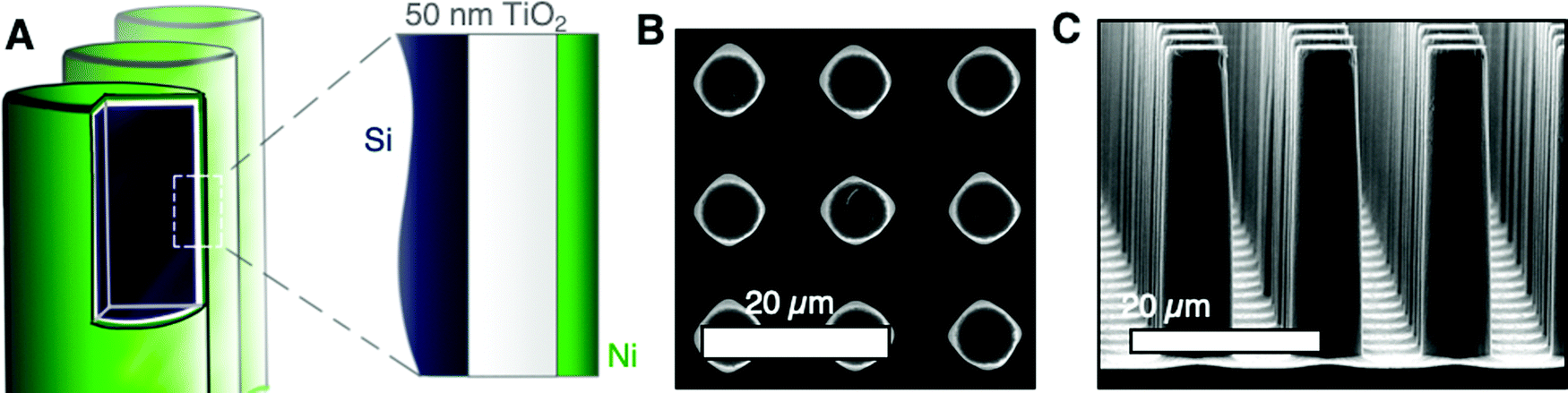 | ||
| Fig. 1 (A) Scheme of n-Si μW/TiO2/Ni electrodes. Si (dark blue) was radially coated with TiO2 (white) via ALD and Ni (green) via sputtering. (B) Plan-view scanning electron micrographs of μW 6|14 n-Si/TiO2/Ni. (C) Cross-section scanning electron micrographs of μW 6|14 n-Si/TiO2/Ni. | ||
The optical effects of O2(g) bubbles on upward-facing electrodes were investigated for electrodes in 1.0 M KOH(aq.). Fig. 2A presents the current density vs. potential, J–E, behavior of n-Si/TiO2/Ni photoanodes under simulated 1 sun conditions, as measured via linear-sweep voltammetry at a scan rate of 200 mV s−1, before and after extended potentiostatic holds at 1.6 V vs. RHE (Fig. 2B). The potential was swept at a rate sufficient to assess the J–E behavior of the photoelectrode in the absence or in the presence of a stable gas bubble layer, while maintaining sufficiently low sweep rates that the charging current did not contribute substantially to J. Data were not corrected for the substantial iR drop between the working and the reference electrode. A representative iR-corrected plot of the J–E behavior of a planar n-Si/TiO2/Ni photoanode, accounting for the potential drop through the 5.3 ohm solution resistance, is provided as Fig. S15 (ESI†). Electrodes were poised at a potential at which J was light-limited, Jph, producing conditions under which efficient charge separation produced by the potential drop across the space-charge region minimized effects due to changes in the exposed catalyst area, concentration overpotential, and/or electrolyte resistance. Gas layers at oxygen-evolving n-Si/TiO2/Ni photoanodes were characterized by large numbers of bubbles that released frequently at small radii. Under simulated 1 sun illumination, Jph was 20 mA cm−2 at either planar or μW 6|14 n-Si/TiO2/Ni photoanodes, which produced streams of bubbles due to nucleation of bubbles predominantly at a small number of sites across the surface (Fig. 2C and D). The number of nucleation sites increased as the illumination intensity increased, leading to a more uniform coverage of bubbles across the photoanode surface (Fig. S4, ESI†). The bubbles at the planar n-Si/TiO2/Ni photoanode were larger in radius than the bubbles produced by μW 6|14 n-Si/TiO2/Ni photoanodes.
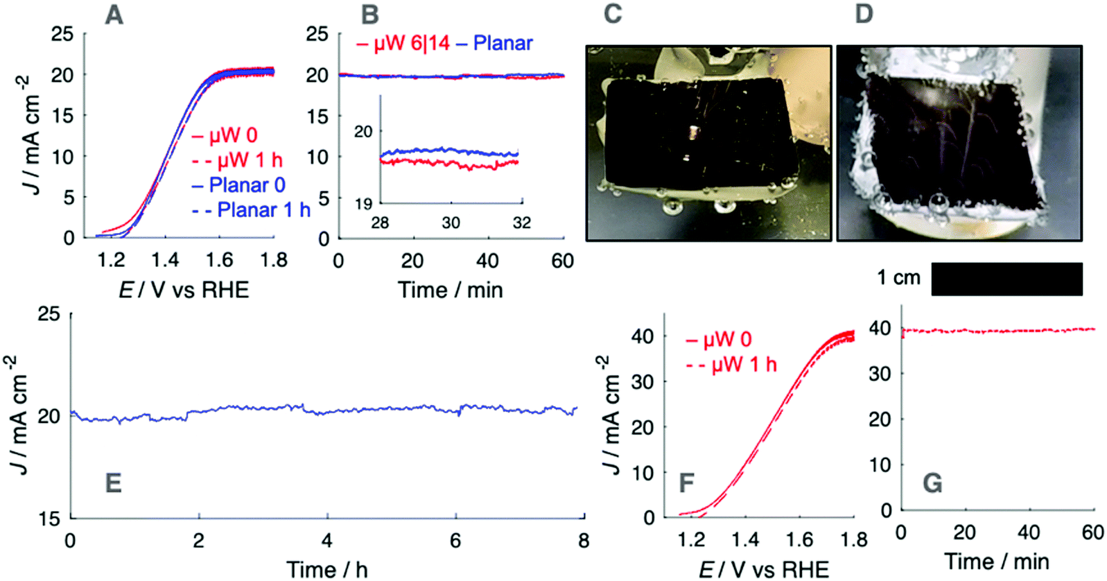 | ||
| Fig. 2 (A) J–E behavior for upward-facing planar (blue) and μW 6|14 (red) n-Si/TiO2/Ni photoanodes in stagnant 1.0 M KOH(aq.) recorded at 200 mV s−1 under illumination from an ELH type W-halogen lamp. Forward scans were recorded before (continuous) and reverse scans were recorded after (dashed) 1 h of continuous O2(g) evolution at 1.6 V vs. RHE. (B) Jph–t behavior for photoanodes in (A), held at 1.6 V vs. RHE. (C and D) Photographs of a planar (D) and μW 6|14 (E) n-Si/TiO2/Ni electrode at Jph = 20 mA cm−2. (E) Extended stability test of a planar n-Si/TiO2/Ni electrode at 1.6 V vs. RHE under illumination from an ELH-type W-halogen lamp in stagnant 1.0 M KOH(aq.). (F) J–E behavior for an upward-facing μW 6|14 n-Si/TiO2/Ni photoanode as in (A) following a doubling of the light intensity. (G) Jph–t behavior of the photoanode in (F) at 1.8 V vs. RHE. | ||
The production of O2(g) bubbles during gas evolution did not lead to a substantial change in Jph, which remained stable and close to the measured maximum during voltammetry (Fig. 2A). This Jph–t behavior did not change during extended testing at 1.6 V vs. RHE (Fig. 2E). Linear-sweep voltammograms after 1 h of continuous photoanodic operation showed that the J–E behavior was not substantially affected by the presence of a sparse gas bubble film. Illumination with 2 suns of intensity yielded similarly stable Jph–t behavior, consistent with the J–E behavior before and immediately after chronoamperometry (Fig. 2F and G). At nominally constant illumination intensities, μW 6|28 n-Si/TiO2/Ni photoanodes yielded lower Jph values than μW 6|14 n-Si/TiO2/Ni photoanodes (Fig. S5, ESI†). The lower Jph at μW 6|28 n-Si/TiO2/Ni photoanodes, in comparison to analogous samples prepared from a μW 6|14 array, was due to the decreased coverage of microwires such that a greater quantity of light was absorbed by the planar substrate. A planar n-Si/TiO2/Ni photoanode with a 10 nm thick layer of Ni exhibited Jph = 17.4 mA cm−2 under 2 suns (Fig. S5A, ESI†).
The effect of gas evolution on the Nernst diffusion layer was quantified for n-Si/TiO2/Ni photoanodes in the presence of a dilute, redox-active tracer, Fe(CN)64−, whose oxidation product, Fe(CN)63− strongly absorbs blue light (Fig. 3A). Measurements were performed on both downward-facing and upward-facing electrodes. During photoanodic operation at 2.1 V vs. RHE, Jph was set by the illumination intensity from the narrow-band red LED, which was primarily reflected or converted to photogenerated charge carriers and thus did not contribute to substantial heating of the electrolyte. The average partial photocurrent passed towards Fe(CN)64− oxidation was calculated from the concentration of Fe(CN)63− measured in the cell after electrolysis. During the forward scan, two anodic peaks were observed, corresponding to surface oxidation of Ni and oxidation of Fe(CN)64−. After electrolysis, these peaks were not present during the reverse scan (Fig. 3B), indicating that the Fe(CN)64− concentration at the surface approached zero and that the electrochemically addressable Ni was fully oxidized. A single, broad reduction wave was observed, consistent with the voltammetric behavior of a polished Ni surface, but with peaks shifted towards more negative potentials as expected for a photoanode (Fig. S6, ESI†). Measurements of the electrochemical behavior of Fe(CN)64− in 1.0 M KOH(aq.) at a Ni wire, for comparison to the n-Si/TiO2/Ni surface, and at a Au wire, to measure the isolated electrochemical behavior of the Fe(CN)63−/4− couple, are presented as Fig. S6 (ESI†).
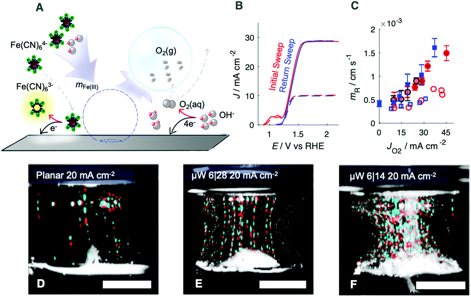 | ||
| Fig. 3 (A) Scheme of diffusion tracer experiments using Fe(CN)64− as a probe. OH− and Fe(CN)64− are brought to the surface via diffusion and bubble-generated microconvection and contribute to faradaic current. (B) J–E behavior of planar n-Si/TiO2/Ni photoanode in 10 mM Fe(CN)64−(aq.), 1.0 M KOH(aq.) before (red) and after (blue) a 5 min potential hold at 2.1 V vs. RHE. (C) Mass-transport velocity as a function of anodic current density towards O2 for planar, blue squares, μW 6|14 n-Si/TiO2/Ni, dark-red circles, and μW 6|28 n-Si/TiO2/Ni, light-red circles, photoanodes in 10 mM Fe(CN)64−(aq.), 1.0 M KOH(aq.). Upward-facing measurements are shown by filled markers whereas downward-facing measurements are shown as open markers. Error bars on upward-facing measurements represent one standard deviation across three independent potential holds. (D–F) False-colored photographs of planar (D), μW 6|28 (E), and μW 6|14 (E) n-Si/TiO2/Ni photoanodes during O2 evolution in 10 mM Fe(CN)64−(aq.), 1.0 M KOH(aq.) at Jph = 20 mA cm−2. Two frames separated by 50 ms were overlaid with changes highlighted in red and cyan, with red pixels representing the first frame and cyan pixels representing the second frame. All scale bars represent 5 mm. | ||
Eqn (1) relates the diffusion-limited current density for Fe(CN)63− production, jFe(III), to the bulk concentration of Fe(CN)64−,  , and the mass-transport velocity, mFe(II), across the diffusion layer.
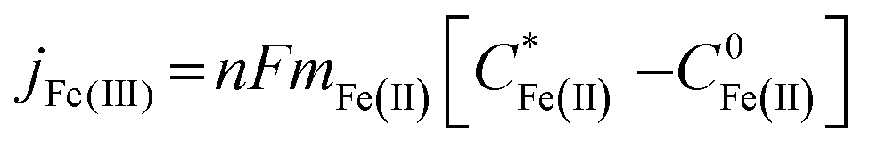 | (1) |
Side-view, false colored photographs of illuminated gas streams emanating from upward-facing photoanodes (Fig. 3D–F) revealed small streams of bubbles that were difficult to observe in top-down images. Original images are available as Fig. S9 (ESI†), and a composite video of the gas streams is provided as Video S1 (ESI†). Fewer, larger bubbles were released on planar n-Si/TiO2/Ni photoanodes (Fig. 3D) than on μW 6|14 or μW 6|28 n-Si/TiO2/Ni photoanodes (Fig. 3E and F). The vertical gas streams at μW 6|14 and μW 6|28 n-Si/TiO2/Ni electrodes generated a horizontal flow of electrolyte at the electrode and at the electrolyte surface. Near the electrode surface, this flow was directed towards the center of the electrode, but at the electrolyte surface the flow was directed towards the edges of the electrode. Jph/Jbareph was nearly constant with time, and for Jph ≤ 30 mA cm−2 the optical losses did not exceed 2% of Jbareph (Fig. S10, ESI†) despite substantial differences in the distribution of gas bubbles in the ∼1 cm thick, illuminated layer of electrolyte.
The radius and coverage of gas bubbles were both small at either upward-facing planar or μW n-Si/TiO2/Ni electrodes, and did not contribute to substantial increases in the ohmic resistance or concentration overpotential (Fig. 2A and F). Moreover, bubbles did not substantially reflect photons away from the semiconductor (Fig. 2B, E and G). The generation of gas bubble streams has been studied at Pt microelectrodes in 1.2 M H2SO4(aq.).19 Gas evolution at upward-facing electrodes consistently led to increased mFe(II) relative to a stagnant electrolyte. Such behavior is consistent with previous measurements of the oxygen-evolving behavior of polished Ni foils.6 The redox-active tracer used herein was present in concentrations that were 100 times more dilute than the concentration of OH− in the cell, but yielded mass-transport-limited jFe(III) values only 10 times less than Jph required for a 10% efficient solar-to-fuels device.4 This behavior suggests that the formation and departure of O2 bubbles on upward-facing photoanodes generates sufficient convection to sustain device operation in unstirred electrolytes.
Mutually similar mFe(II) values were observed at upward-facing planar, μW 6|14, and μW 6|28 photoanodes (Fig. 3D–F), despite the variation in the number density and radii of bubbles in the gas-layers. The dependence of mass-transport velocities only on the volumetric flow rate of gas, and not the size or distribution of gas bubbles, is consistent with a fluid replacement model for bubble-generated microconvection.6,20 Mass-transport velocities were lower at downward-facing electrodes relative to upward-facing electrodes (Fig. 3C), suggesting that the departure rate of gas bubbles from the surface is a controlling variable on the microconvection process. A consequence of this microconvection model is that electrodes that produce isolated streams of gas bubbles (Fig. 3D and E) will produce a spatially nonuniform distribution of products and reactants, potentially leading to undesirable pH gradients and efficiency losses. Increases in the density of microwires, from planar to μW 6|28 to μW 6|14, led to decreases in the radii of bubbles and an increased number of gas streams, which would be expected to lead to more uniform mass transport. Preexisting gas nuclei can also be added to the surface to ensure a more even distribution of passive microconvection.21 Solar fuels devices should ensure that the quantity of gas that is collected within gas bubbles approaches unity, to minimize concentration overpotentials and maximize the mass-transport velocity at the surface. We have herein evaluated the effects of microconvection due to bubble formation, noting that convection due to thermal gradients may be important for solar fuels devices under concentrated sunlight (ESI†). Under nonconcentrated sunlight, the generation of highly reduced products such as C2H4 (12 e− per mole) may not produce sufficient gas flow rates to eliminate the need for external convection at that electrode surface.
The low gas coverages and minimal decreases in Jph in stagnant electrolytes observed for upward-facing Si photoanodes in 1.0 M KOH(aq.) contrast with the previously reported behavior of side-facing or upward-facing planar Si photocathodes in H2SO4(aq.), which exhibited greater coverages of larger bubbles than observed herein.9,13 The surface chemistry of planar photoelectrodes influences the gas coverage and consequently affects Jph. The shape and departure diameter of a bubble is controlled by the adhesive forces at the solid/gas interface. The differences in Rb and θb between upward-facing photocathodes and photoanodes observed herein are not explained by differences in the surface free energy; both the hydrated Ni(OH)2/NiOOH, which forms during photoanodic operation in 1.0 M KOH(aq.), and clean noble metal surfaces, are expected to act as wettable, high-energy surfaces.22,23 However, a monolayer of carbon contamination is sufficient to increase the hydrophobicity of a metal surface, and advancing water droplet contact angles >50° have been reported at Au and Pt.24 Rigorous cleaning may be required to observe similar nucleation rates at Si coated with a uniform layer of Pt. Hydroxyl terminated Si, Si/OH, is wettable and thus is expected to exhibit bubble contact angles approaching 180°.
Upward facing p-Si photocathodes in 0.50 M H2SO4(aq.)
To evaluate the gas-evolving behavior in the absence of the Ni catalyst layer as well in the absence of the TiO2 protection layer, upward-facing photocathodes prepared from planar p-Si were used as hydrogen-evolving photocathodes in 0.50 M H2SO4(aq.). Photoanodes prepared from bare Si rapidly formed passivating SiOx under anodic conditions. The J–E behaviors of upward-facing planar p-Si/OH and p-Si/H photocathodes in 0.50 M H2SO4(aq.) were recorded using linear sweep voltammetry at 200 mV s−1 (Fig. 4A). Fig. 4B presents the time-dependent behavior of Jph at upward-facing p-Si photocathodes maintained at E = −2.2 V vs. RHE, which produced light-limited cathodic current densities. Jph at upward-facing planar p-Si/OH electrodes was nearly identical to Jbareph, consistent with the absence of surface-attached gas bubbles (Fig. 4C). In contrast, an upward-facing p-Si/H photocathode exhibited up to a 10% reduction to Jph concurrent with a substantial coverage of gas bubbles on the electrode surface (Video S2, ESI†). The radius and coverage of gas bubbles at p-Si/H photocathodes decreased with time and was accompanied by a gradual increase in Jph.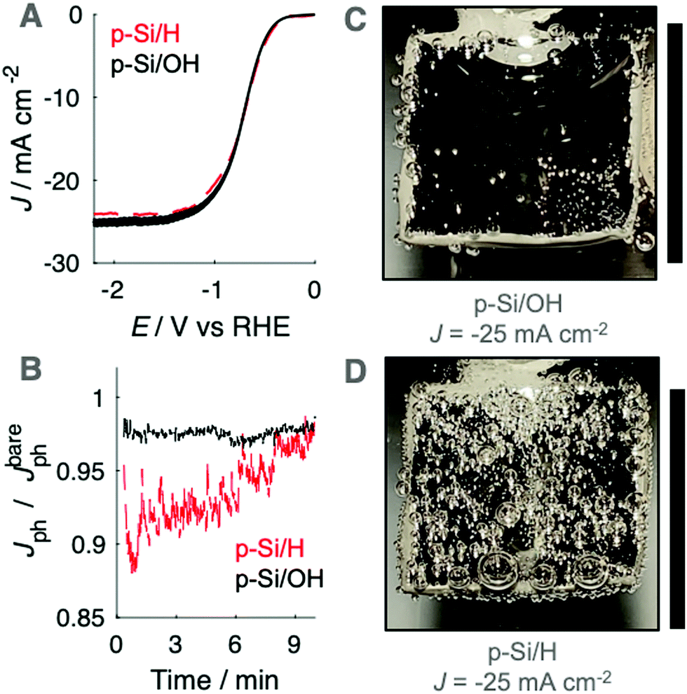 | ||
| Fig. 4 (A) J–E behavior for upward-facing p-Si photocathodes in stagnant 0.50 M H2SO4(aq.) recorded at 200 mV s−1 under illumination from an ELH lamp. (B) J–t behavior for photoanodes in (A) at −2.2 V vs. RHE in 0.50 M H2SO4(aq.). Top-down photographs of an (C) RCA-cleaned and (D) HF-cleaned planar p-Si photocathode. Scale bars represent 1 cm. | ||
A substantial reduction in the gas coverage was observed for hydroxyl-terminated upward-facing p-Si surfaces in 0.50 M H2SO4(aq.) relative to hydride-terminated surfaces. This observation is consistent with heterogeneous nucleation rate models that include a dependence on the contact angle of the initial nuclei, because surfaces with θb ∼ 180° are not catalytic for heterogeneous nucleation.25–27 (100)-Oriented Si surfaces terminated with Si–H bonds, following exposure to HF(aq.), exhibit an advancing water contact angle >70°,28 and p-Si photocathodes dipped in HF exhibited gas coverages and Jph losses in 0.50 M H2SO4(aq.) that were comparable to those of Si coated with Ti/Pt.13 For planar solar fuels devices that utilize a noble metal catalyst layer such Au or Pt, small Rb and θb values, approaching 180°, may be obtained after careful cleaning of such electrodes. Upward-facing polished Pt foils primarily produced bubbles of Rb < 50 μm after three days of continuous cathodic current flow in 1.0 M H2SO4(aq.). Microstructuring or micropatterning can alleviate the deleterious effects of gas bubbles produced by non-optimal surface chemistry. Hence the results described herein are consistent with prior reports that the capillary forces within Si μW arrays, attributed to the more frequent release of small bubbles, lead to stable (photo)electrochemical performance in the absence of external convection.8,29 Patterned catalyst islands surrounded by a hydrophilic, passivating metal oxide layer could also result in increased wettability and decreased departure diameters for gas bubbles on upward-facing electrodes.
Ray-tracing simulations of surface attached bubbles
Fig. 5 summarizes the results of ray-tracing simulations of the optical characteristics of bubbles attached to crystalline-Si electrodes under 630 nm, unpolarized light. Fig. 5A presents the normalized, theoretically predicted (*) light-limited photocurrent density, as a function of the radial position, r for a ray of infinitesimal thickness. Simulated data were normalized to
  predicted at a solid/liquid interface at normal incidence, Jbareph. A global minimum in Jph(r) should occur in a narrow ring at which total internal reflection at the liquid/gas interface directs rays away from the absorber. In contrast, a wider, local minimum in Jph(r) should occur for rays incident on the region above the solid/gas interface (Fig. 5E). Bubbles with a large contact angle, θb, (Fig. 5E) minimize the area of the solid/gas interface and should consequently reduce the magnitude of optical losses resulting from gas coverage. The simulations indicated a global maximum in
  observed for bubbles with θb = 160°, but not with θb = 120°, due to a large number of reflections in the water layer adjacent to the solid/gas interface. Reductions in Jph primarily result from reflections at the solid/gas interface, because reflected and refracted rays at the liquid/gas interface are predominately directed downwards towards the absorber.
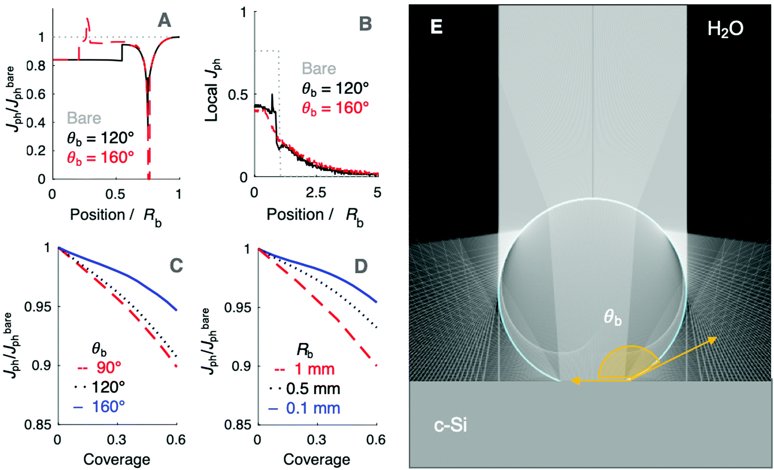 | ||
| Fig. 5 (A) Simulated Jph(r) profile at a single bubble, for varied θb, normalized to the simulated Jbareph at the bare solid/liquid interface. (B) Distribution of Jph(r) as measured via binned light absorption during ray-tracing simulations. The absorption is recorded as a function of position and the signal at individual bins was normalized to the total power incident on each bin in the absence of reflections or refractions. (C) Total Jph at a 1 cm wide electrode as a function of gas coverage for bubbles with Rb = 250 μm and various values of θb. (D) Total Jph at a 1 cm wide electrode as a function of gas coverage of evenly-spaced bubbles with θb = 160° and various values of Rb. (E) Results of a ray-tracing simulation at a single surface-attached gas bubble, with θb = 160°, on crystalline Si, illuminated by 630 nm unpolarized light, with liquid water as the surrounding medium. | ||
The simulations also revealed that gas bubbles should produce a substantial redistribution of photogenerated carriers in the electrode (Fig. 5B). Bubbles act as diverging lenses that should reduce the Jph under the bubble, |r| < Rb and divert intensity to outside the bubble, |r| > Rb. The highest regions of increased photocurrent were directly beyond the projected radius of a surface-attached bubble, with complementary effects for neighboring bubbles (Fig. S11, ESI†). The sum total effect of gas films that contained multiple bubbles was simulated by line-scans over a 1 cm wide absorber, while varying the total coverage by bubbles having a uniform size and shape. Bubbles with larger values of θb minimized the area of the gas/solid interface for an equivalent projected surface coverage, producing values of  close to Jbareph (Fig. 5C). Larger bubbles scattered light from a greater distance from the absorber surface and thus led to increased optical losses relative to an equivalent surface coverage of smaller bubbles (Fig. 5D). However, gas coverages ≤0.5 produced a <10% reduction in simulated Jph values.
The close agreement between line scans of  simulated in this work and previously reported Jph(r) line scans measured experimentally using scanning-photocurrent microscopy demonstrates that ray-tracing simulations are an accurate method for simulating the optical properties of bubbles that have diameters substantially larger than a wavelength of light.13 Although the shape of surface-attached bubbles can be expected to affect the spatial propagation of off-incident illumination (Fig. 5B), Jph should be close to Jbareph if Rb is small with respect to the electrode width (Fig. 5D). Refracted rays are not scattered far from a bubble and can moreover produce an increase in collection efficiency relative to the absorption at a bare-Si/liquid interface (Fig. 5A). Eqn (2) gives the scattering distance, s, for a ray at position r undergoing total internal reflection as a function of the bubble radius, Rb, and θb:
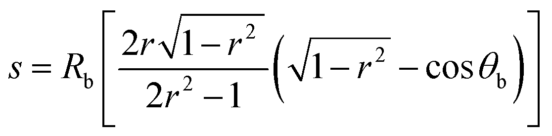 | (2) |
Downward-facing photoelectrodes
To quantitatively evaluate the optical effects of static gas bubble films at the photoelectrode surface while controlling for the effect of departing gas bubbles in the electrolyte layer, the photoelectrochemical characteristics of downward-facing electrodes were investigated using 630 nm illumination. The gas coverage was measured from photographs and was compared against the instantaneous Jph value determined directly before the gas coverage measurement (Fig. S13, ESI†). Mutually equivalent rates of gas production were obtained by maintaining Jbareph at −5 mA cm−2 for photocathodes (2 e− H2 production) and at 10 mA cm−2 for photoanodes (4 e− O2 production). Downward-facing planar and μW p-Si photocathodes exhibited larger bubble coverages than downward-facing n-Si/TiO2/Ni photoanodes (Fig. 6). A maximum coverage of 0.57 was observed at downward-facing electrodes in 0.50 M H2SO4 with a minimum Jph/Jbareph of 0.80 and 0.81 observed at p-Si and n+p-Si/Ti/Pt electrodes, respectively (Fig. 6A). The minimum Jph/Jbareph value at downward-facing planar and μW 6|14 n-Si/TiO2/Ni photoanodes was 0.96 and 0.94, respectively (Fig. 6B).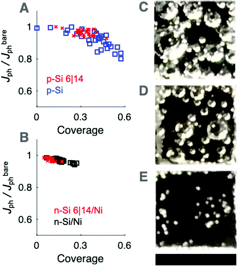 | ||
| Fig. 6 Coverage vs. Jph/Jbareph for downward-facing (A) hydrogen-evolving photocathodes in 0.50 M H2SO4(aq.) and (B) oxygen-evolving photoanodes in 1.0 M KOH(aq.). (C–E) Representative images of planar p-Si (C), μW 6|14 p-Si (D), and n-Si/Ni (E). Scale bars represents 5 mm. | ||
The dependence of Jph/Jbareph on the gas coverage (Fig. 6A and B) was in agreement with simulated Jph/Jbareph data vs. coverage data for 2D line scans at coverages <0.4 (Fig. 5C and D). At the highest gas coverages, the experimentally measured Jph/Jbareph values were lower than the Jph/Jbareph values predicted by simulation, concurrent with the presence of the largest gas bubbles. The simulated gas coverages however assumed an even distribution of gas bubbles across the surface, whereas in practice gas bubbles tended to aggregate and were more often found near the edges of the electrode, which could increase the amount of light scattered away from the absorber. Differences in the shape of larger bubbles due to hydrostatic pressure could also influence the measured optical effects, but such effects are not expected to be relevant to the optical properties of bubbles at upward-facing electrodes.
The ray-tracing simulations described herein assumed that only bubbles that are large with respect to the wavelength of light contributed substantially to optical losses in photoelectrochemical cells. This assumption is justified by the R ∼ t1/2 dependence of bubble growth, such that bubbles spend a short time as small nuclei but spend a relatively long time close to the Rb at which the bubbles leave the surface.30 The simulations in this work do not treat interference effects and will underestimate the effective scattering radius of small bubbles.31 These effects could be important for solar fuels devices that generate a large number of small gas nuclei due to operation under concentrated sunlight. The dominant optical effect of gas bubbles is the spatial redistribution of photogenerated carriers across the semiconductor surface. The deleterious effects of bubbles on the efficiency of small-scale photoelectrochemical solar fuels devices suitable for research-scale measurements cells are not present on larger-scale electrodes.10 Solar fuels devices using a conductive emitter layer will redistribute carriers across the equipotential top surface such that bubbles will not affect the local Jph.32 Gas bubbles that are much smaller than the carrier-collection length of a semiconductor are unlikely to influence the spatial distribution of Jph because photogenerated carriers will redistribute to minimize the overpotential at individual catalyst sites. Large gas bubbles on membrane-embedded, electrically isolated microcells will have more substantial effects on the device efficiency if cells operating under less than 1 sun illumination do not generate sufficient photovoltage to drive the full-cell reaction. Gas bubbles that adhere to micropatterned catalyst sites will direct light away from the catalyst, which could lead to beneficial increases in the total Jph.
Tandem photocathodes connected to a dark RuOx anode have been reported to exhibit lower stability and efficiency in two-electrode configurations relative to three-electrode configurations.33 The contributions of gas bubbles to the solution resistance, concentration overpotential, and mass transport velocity are expected to be mutually similar for optimally configured two-electrode and three-electrode measurements. If bubbles do not obstruct current carrying paths, the solution resistance during wireless water splitting should be lower, and thus more favorable for stability and efficiency, than in the three-electrode configuration used herein. Deleterious effects in a two-electrode configuration of cross-contamination of impurities produced by the counter electrode that may degrade the performance of the working photoelectrode are minimized in our three-electrode configuration and could be minimized in a two-electrode configuration through optimal choice of the counter electrode material and electrolyte, along with optimization of cell design including membranes or separators.
Conclusions
Simulations and experimental data confirm that forward-scattering optical effects of bubbles do not substantially affect the total Jph of a photoelectrochemical cell if Rb of the bubbles are kept small prior to departure from the surface. Careful preparation of metal and semiconductor surfaces could lead to θb approaching 180°, which leads to reduced area for surface reflections, lowers the gas coverage, and minimizes Rb. Solar fuels device designs should thus seek to maximize the wettability of the top-facing photoelectrode surface via control of the surface chemistry and/or microstructure, to obviate the need for surfactants such as Triton X-100 in the electrolyte.11 Planar and microstructured n-Si/TiO2/Ni photoanodes, ∼1 cm2 in area, exhibit gas coverages characterized by small Rb and large θb, and such devices exhibited minimal changes to Jph during operation under 1 sun equivalent illumination. Although the gas coverage increased substantially as the illumination intensity increased, Jph remained stable with time. Gas evolution at upward-facing photoanodes in 1.0 M KOH(aq.) led to increased mass-transport velocities compared to a stagnant electrolyte, and produces minimal concentration overpotentials adequate to facilitate efficient solar fuels device operation under non-concentrated sunlight, thereby eliminating the need for external convection. Previously, H2(g) bubbles at downward-facing dark cathodes have been shown to lead to small increases in cell resistance while reducing concentration overpotentials and increasing local convection in stagnant electrolytes.8 The present study shows that O2(g) bubbles with small Rb at upward-facing, cm-scale illuminated photoelectrodes do not impede light-absorption while similarly contributing to increases to the mass-transport velocity in the electrolyte. Thus, modest coverages of small gas bubbles at upward-facing photoelectrodes can provide a net benefit to the performance of solar fuels devices.Author contributions
Si-μW Fabrication, P. A. K., Metallization, Z. P. I., Atomic Layer Deposition, W. Y., Scanning-Electron Microscopy, A. I. C., Investigation, P. A. K.; Writing – Original Draft, P. A. K. and N. S. L., Writing – Review and Editing, P. A. K., N. S. L., Z. P. I., W. Y., A. I. C., Funding Acquisition, N. S. L. Supervision, N. S. L.Conflicts of interest
The authors declare no competing interests.Acknowledgements
This material is based upon work performed by the Joint Center for Artificial Photosynthesis, a DOE Energy Innovation Hub, supported through the Office of Science of the U.S. Department of Energy under Award No. DE-SC0004993. Silicon microwire arrays were fabricated in the Kavli Nanoscience Institute (KNI) at Caltech; we thank the KNI staff for their assistance with fabrication. We are grateful to Rick Gerhart for assistance in fabricating glassware for solar simulations. Additional instrumentation was provided by the Molecular Materials Research Center in the Beckman Institute at Caltech. We appreciate Bruce Brunschwig for providing helpful feedback on the manuscript.References
- J. W. Ager, M. R. Shaner, K. A. Walczak, I. D. Sharp and S. Ardo, Energy Environ. Sci., 2015, 8, 2811–2824 RSC.
- J. A. Leistra and P. J. Sides, J. Electrochem. Soc., 1987, 134, 2442–2446 CrossRef CAS.
- R. H. Coridan, Z. G. Schichtl, T. Sun and K. Fezzaa, ACS Appl. Mater. Interfaces, 2016, 8, 24612–24620 CrossRef CAS.
- R. H. Coridan, A. C. Nielander, S. A. Francis, M. T. McDowell, V. Dix, S. M. Chatman and N. S. Lewis, Energy Environ. Sci., 2015, 8, 2886–2901 RSC.
- A. Angulo, P. van der Linde, H. Gardeniers, M. Modestino and D. F. Rivas, Joule, 2020, 4, 555–579 CrossRef CAS.
- L. Janssen and J. Hoogland, Electrochim. Acta, 1973, 18, 543–550 CrossRef CAS.
- P. Boissonneau and P. Byrne, J. Appl. Electrochem., 2000, 30, 767–775 CrossRef CAS.
- P. A. Kempler, R. H. Coridan and N. S. Lewis, Energy Environ. Sci., 2020, 13, 1808–1817 RSC.
- S. S. Kocha, D. Montgomery, M. W. Peterson and J. A. Turner, Sol. Energy Mater. Sol. Cells, 1998, 52, 389–397 CrossRef CAS.
- E. Verlage, S. Hu, R. Liu, R. J. Jones, K. Sun, C. Xiang, N. S. Lewis and H. A. Atwater, Energy Environ. Sci., 2015, 8, 3166–3172 RSC.
- O. Khaselev and J. A. Turner, Science, 1998, 280, 425–427 CrossRef CAS.
- G. E. Davis, J. Opt. Soc. Am. A, 1955, 45, 572–581 CrossRef.
- A. E. Dorfi, A. C. West and D. V. Esposito, J. Phys. Chem. C, 2017, 121, 26587–26597 CrossRef CAS.
- A. J. Leenheer and H. A. Atwater, J. Electrochem. Soc., 2010, 157, B1290 CrossRef CAS.
- I. Holmes-Gentle, F. Bedoya-Lora, F. Alhersh and K. Hellgardt, J. Phys. Chem. C, 2018, 123, 17–28 CrossRef.
- W. Kern, J. Electrochem. Soc., 1990, 137, 1887 CrossRef CAS.
- K. Osseo-Asare, D. Wei and K. K. Mishra, J. Electrochem. Soc., 1996, 143, 749 CrossRef CAS.
- S. Hu, M. R. Shaner, J. A. Beardslee, M. Lichterman, B. S. Brunschwig and N. S. Lewis, Science, 2014, 344, 1005–1009 CrossRef CAS.
- D. Fernandez, P. Maurer, M. Martine, J. Coey and M. E. Möbius, Langmuir, 2014, 30, 13065–13074 CrossRef CAS.
- H. Vogt and K. Stephan, Electrochim. Acta, 2015, 155, 348–356 CrossRef CAS.
- P. Peñas, P. van der Linde, W. Vijselaar, D. van der Meer, D. Lohse, J. Huskens, H. Gardeniers, M. A. Modestino and D. F. Rivas, J. Electrochem. Soc., 2019, 166, H769 CrossRef.
- L. Trotochaud, S. L. Young, J. K. Ranney and S. W. Boettcher, J. Am. Chem. Soc., 2014, 136, 6744–6753 CrossRef CAS.
- T. Smith, J. Colloid Interface Sci., 1980, 75, 51–55 CrossRef CAS.
- R. A. Erb, J. Phys. Chem., 1965, 69, 1306–1309 CrossRef CAS.
- S. Lubetkin, Chem. Soc. Rev., 1995, 24, 243–250 RSC.
- S. R. German, M. A. Edwards, H. Ren and H. S. White, J. Am. Chem. Soc., 2018, 140, 4047–4053 CrossRef CAS.
- A. M. Soto, S. R. German, H. Ren, D. van der Meer, D. Lohse, M. A. Edwards and H. S. White, Langmuir, 2018, 34, 7309–7318 CrossRef CAS.
- Z. Cui and C. G. Takoudis, J. Electrochem. Soc., 2003, 150, G694 CrossRef CAS.
- D. V. Esposito, Y. Lee, H. Yoon, P. M. Haney, N. Y. Labrador, T. P. Moffat, A. A. Talin and V. A. Szalai, Sustainable Energy Fuels, 2017, 1, 154–173 RSC.
- P. van der Linde, P. Peñas-López, Á. M. Soto, D. van der Meer, D. Lohse, H. Gardeniers and D. F. Rivas, Energy Environ. Sci., 2018, 11, 3452–3462 RSC.
- D. L. Kingsbury and P. L. Marston, J. Opt. Soc. Am. A, 1981, 71, 358–361 CrossRef.
- E. L. Warren, S. W. Boettcher, M. G. Walter, H. A. Atwater and N. S. Lewis, J. Phys. Chem. C, 2011, 115, 594–598 CrossRef CAS.
- J. L. Young, M. A. Steiner, H. Döscher, R. M. France, J. A. Turner and T. G. Deutsch, Nat. Energy, 2017, 2, 17028 CrossRef CAS.
Footnote |
| † Electronic supplementary information (ESI) available. See DOI: 10.1039/d0ee02796k |
| This journal is © The Royal Society of Chemistry 2021 |